WM9712L
AC'97 Audio and Touchpanel CODEC
WOLFSON MICROELECTRONICS plc
www.wolfsonmicro.com
Production Data, December 2003, Rev 4.0
Copyright
2003 Wolfson Microelectronics plc.
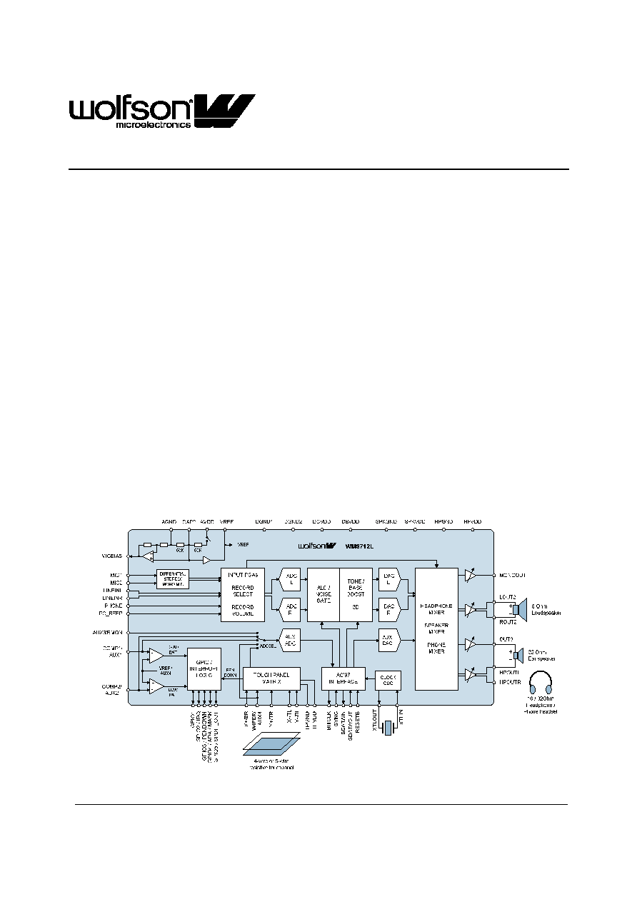
DESCRIPTION
The WM9712L is a highly integrated input / output device
designed for mobile computing and communications. The
device can connect directly to a 4-wire or 5-wire touchpanel,
mono or stereo microphones, stereo headphones and a
mono speaker, reducing total component count in the
system. Additionally, phone input and output pins are
provided
for
seamless
integration
with
wireless
communication devices.
The WM9712L also offers up to four auxiliary ADC inputs
for analogue measurements such as temperature or light,
and five GPIO pins for interfacing to buttons or other digital
devices. To monitor the battery voltage in portable systems,
the WM9712L has two uncommitted comparator inputs.
All device functions are accessed and controlled through a
single AC-Link interface compliant with the AC'97 standard.
Additionally, the WM9712L can generate interrupts to
indicate pen down, pen up, availability of touchpanel data,
low battery, dead battery, and GPIO conditions.
The WM9712L operates at supply voltages from 1.8 to 3.6
Volts. Each section of the chip can be powered down under
software control to save power. The device is available in a
small leadless 7x7mm QFN package, ideal for use in hand-
held portable systems, or in the industry standard 48-pin
TQFP package.
FEATURES
∑
AC'97 Rev 2.2 compatible stereo codec
- DAC SNR 94dB, THD ≠87dB
- ADC SNR 92dB, THD ≠87dB
- Variable Rate Audio, supports all WinCE sample rates
- Tone Control, Bass Boost and 3D Enhancement
∑
On-chip 45mW headphone driver
∑
On-chip 400mW mono speaker driver
∑
Stereo, mono or differential microphone input
- Automatic Level Control (ALC)
∑
Auxiliary mono DAC (ring tone or DC level generation)
∑
Seamless interface to wireless chipset
∑
Resistive touchpanel interface
- Supports 4-wire and 5-wire panels
- 12-bit resolution, INL
±
2 LSBs (<0.5 pixels)
- X, Y and touch-pressure (Z) measurement
- Pen-down detection supported in Sleep Mode
∑
Up to 5 GPIO pins
∑
2 comparator inputs for battery monitoring
∑
Up to 4 auxiliary ADC inputs
∑
1.8V to 3.6V supplies
∑
7x7mm QFN or 48-pin TQFP package options
APPLICATIONS
∑
Personal Digital Assistants (PDA)
∑
Smartphones
∑
Handheld and Tablet Computers
BLOCK DIAGRAM

WM9712L
Production Data
w
PD Rev 4.0 December 2003
2
TABLE OF CONTENTS
DESCRIPTION .......................................................................................................1
FEATURES.............................................................................................................1
APPLICATIONS .....................................................................................................1
BLOCK DIAGRAM .................................................................................................1
TABLE OF CONTENTS .........................................................................................2
PIN CONFIGURATION...........................................................................................4
ORDERING INFORMATION ..................................................................................4
PIN DESCRIPTION ................................................................................................5
ABSOLUTE MAXIMUM RATINGS .........................................................................6
RECOMMENDED OPERATING CONDITIONS .....................................................6
ELECTRICAL CHARACTERISTICS ......................................................................7
AUDIO OUTPUTS.......................................................................................................... 7
AUDIO INPUTS.............................................................................................................. 8
AUXILIARY MONO DAC (AUXDAC).............................................................................. 8
TOUCHPANEL AND AUXILIARY ADC .......................................................................... 9
COMPARATORS ........................................................................................................... 9
REFERENCE VOLTAGES ........................................................................................... 10
DIGITAL INTERFACE CHARACTERISTICS................................................................ 10
HEADPHONE / SPEAKER OUTPUT THD VERSUS POWER ..................................... 11
POWER CONSUMPTION............................................................................................ 12
DEVICE DESCRIPTION .......................................................................................13
INTRODUCTION.......................................................................................................... 13
AUDIO PATHS OVERVIEW......................................................................................... 14
AUDIO INPUTS ....................................................................................................15
LINE INPUT ................................................................................................................. 15
MICROPHONE INPUT................................................................................................. 15
PHONE INPUT............................................................................................................. 17
PCBEEP INPUT ........................................................................................................... 18
AUDIO ADC..........................................................................................................19
RECORD SELECTOR ................................................................................................. 20
RECORD GAIN............................................................................................................ 21
AUTOMATIC LEVEL CONTROL.................................................................................. 22
AUDIO DACS .......................................................................................................25
STEREO DAC.............................................................................................................. 25
AUXILIARY DAC.......................................................................................................... 28
ANALOGUE AUDIO OUTPUTS ...........................................................................29
HEADPHONE OUTPUTS ≠ HPOUTL AND HPOUTR.................................................. 29
EAR SPEAKER OUTPUT ≠ OUT3............................................................................... 30
LOUDSPEAKER OUTPUTS ≠ LOUT2 AND ROUT2.................................................... 31
PHONE OUTPUT (MONOOUT)................................................................................... 32
THERMAL SENSOR .................................................................................................... 32
JACK INSERTION AND AUTO-SWITCHING............................................................... 33
DIGITAL AUDIO (SPDIF) OUTPUT ............................................................................. 34
AUDIO MIXERS ........................................................................................................... 35

Production Data
WM9712L
w
PD Rev 4.0 December 2003
3
VARIABLE RATE AUDIO / SAMPLE RATE CONVERSION ...............................37
TOUCHPANEL INTERFACE................................................................................38
PRINCIPLE OF OPERATION - FOUR-WIRE TOUCHPANEL ..................................... 38
PRINCIPLE OF OPERATION - FIVE-WIRE TOUCHPANEL........................................ 40
CONTROLLING THE TOUCHPANEL DIGITISER ....................................................... 42
AUXILIARY ADC INPUTS ....................................................................................47
BATTERY MEASUREMENT USING THE BMON/AUX3 PIN ....................................... 47
BATTERY ALARM AND ANALOGUE COMPARATORS ....................................48
GPIO AND INTERRUPT CONTROL ....................................................................51
AC97 DATA AND CONTROL INTERFACE .........................................................58
INTERFACE PROTOCOL............................................................................................ 58
INTERFACE TIMING ................................................................................................... 59
REGISTER MAP...................................................................................................62
REGISTER BITS BY ADDRESS .................................................................................. 63
APPLICATIONS INFORMATION .........................................................................71
RECOMMENDED EXTERNAL COMPONENTS........................................................... 71
LINE OUTPUT ............................................................................................................. 72
AC-COUPLED HEADPHONE OUTPUT....................................................................... 73
DC COUPLED (CAPLESS) HEADPHONE OUTPUT ................................................... 73
BTL LOUDSPEAKER OUTPUT ................................................................................... 74
COMBINED HEADSET / BTL EAR SPEAKER............................................................. 74
COMBINED HEADSET / SINGLE-ENDED EAR SPEAKER......................................... 74
JACK INSERT DETECTION ........................................................................................ 75
HOOKSWITCH DETECTION....................................................................................... 75
PACKAGE DRAWING - QFN ...............................................................................76
PACKAGE DRAWING ≠ TQFP ............................................................................77
IMPORTANT NOTICE ..........................................................................................78
ADDRESS:................................................................................................................... 78
WM9712L
Production Data
w
PD Rev 4.0 December 2003
4
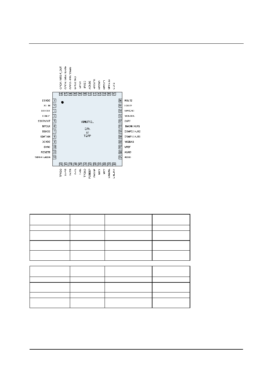
PIN CONFIGURATION
ORDERING INFORMATION
DEVICE
TEMP. RANGE
PACKAGE
MOISTURE LEVEL
SENSITIVITY
WM9712LEFT/V
-25 to +85
o
C
48-pin TQFP
MSL1
WM9712LSEFT/V
-25 to +85
o
C
48-pin TQFP
(lead free)
MSL1
WM9712LEFT/RV
-25 to +85
o
C
48-pin TQFP
(tape & reel)
MSL1
WM9712LSEFT/RV
-25 to +85
o
C
48-pin TQFP
(lead free, tape and reel)
MSL1
DEVICE
TEMP. RANGE
PACKAGE
MOISTURE LEVEL
SENSITIVITY
WM9712LEFL/V
-25 to +85
o
C
48-pin QFN
MSL3
WM9712LSEFL/V
-25 to +85
o
C
48-pin QFN
(lead free)
MSL3
WM9712LEFL/RV
-25 to +85
o
C
48-pin QFN (tape & reel)
MSL3
WM9712LSEFL/RV
-25 to +85
o
C
48-pin QFN
(lead free, tape and reel)
MSL3
Note:
Reel quantity = 2,200

Production Data
WM9712L
w
PD Rev 4.0 December 2003
5
PIN DESCRIPTION
PIN
NAME
TYPE
DESCRIPTION
1
DBVDD
Supply
Digital I/O Buffer Supply
2
XTLIN
Digital Input
Clock Crystal Connection 1 / External Clock Input
3
XTLOUT
Digital Output
Clock Crystal Connection 2
4
DGND1
Supply
Digital Ground (return path for both DCVDD and DBVDD)
5
SDATAOUT
Digital Input
Serial Data Output from Controller / Input to WM9712L
6
BITCLK
Digital Output
Serial Interface Clock Output to Controller
7
DGND2
Supply
Digital Ground (return path for both DCVDD and DBVDD)
8
SDATAIN
Digital Output
Serial Data Input to Controller / Output from WM9712L
9
DCVDD
Supply
Digital Core Supply
10
SYNC
Digital Input
Serial Interface Synchronisation Pulse from Controller
11
RESETB
Digital Input
Reset (asynchronous, active Low, resets all registers to their default)
12
WIPER / AUX4
Analogue Input
Top Sheet Connection for 5-wire Touchpanels / Auxiliary ADC Input
13
TPVDD
Supply
Touchpanel Driver Supply
14
X+/BR
Analogue Input
Touchpanel Connection: X+ (Right) for 4-wire / bottom right for 5-wire
15
Y+/TR
Analogue Input
Touchpanel Connection: Y+ (Top) for 4-wire / top right for 5-wire
16
X-/TL
Analogue Input
Touchpanel Connection: X- (Left) for 4-wire / top left for 5-wire
17
Y-/BL
Analogue Input
Touchpanel Connection: Y- (Bottom) for 4-wire / bottom left for 5-wire
18
TPGND
Supply
Touchpanel Driver Ground
19
PCBEEP
Analogue Input
Line Input to analogue audio mixers, typically used for beeps
20
PHONE
Analogue Input
Phone Input (RX)
21
MIC1
Analogue Input
Left Microphone or Microphone 1 Input
22
MIC2
Analogue Input
Right Microphone or Microphone 2 Input
23
LINEINL
Analogue Input
Left Line Input
24
LINEINR
Analogue Input
Right Line Input
25
AVDD
Supply
Analogue Supply (feeds audio DACs, ADCs, PGAs, mic boost,
mixers)
26
AGND
Supply
Analogue Ground
27
VREF
Analogue Output
Internal Reference Voltage (buffered CAP2)
28
MICBIAS
Analogue Output
Bias Voltage for Microphones (buffered CAP2
◊
1.8)
29
COMP1 / AUX1
Analogue Input
Comparator 1 (dead battery alarm) / Auxiliary ADC Input 1
30
COMP2 / AUX2
Analogue Input
Comparator 2 (low battery alarm) / Auxiliary ADC Input 2
31
BMON / AUX3
Analogue Input
Battery Monitor Input / Auxiliary ADC Input 3
32
CAP2
Analogue In / Out
Internal Reference Voltage (normally AVDD/2, if not overdriven)
33
MONOOUT
Analogue Output
Mono Output, intended for Phone TX signal
34
SPKGND
Supply
Speaker Ground (feeds output buffers on pins 35 and 36)
35
LOUT2
Analogue Output
Left Output 2 (Speaker, Line or Headphone)
36
ROUT2
Analogue Output
Right Output 2 (Speaker, Line or Headphone)
37
OUT3
Analogue Output
Analogue Output 3 (from AUXDAC or headphone pseudo-ground)
38
SPKVDD
Supply
Speaker Supply (feeds output buffers on pins 35 and 36)
39
HPOUTL
Analogue Output
Headphone Left Output
40
HPGND
Supply
Headphone Ground (feeds output buffers on pins 37, 39, 41)
41
HPOUTR
Analogue Output
Headphone Left Output
42
AGND2
Supply
Analogue Ground, Chip Substrate
43
HPVDD
Supply
Headphone Supply (feeds output buffers on pins 37, 39, 41)
44
GPIO1
Digital In / Out
GPIO Pin 1
45
GPIO2 / IRQ
Digital In / Out
GPIO Pin 2 or IRQ (Interrupt Request) Output
46
GPIO3 / PENDOWN
Digital In / Out
GPIO Pin 3 or Pen Down Output
47
GPIO4 / ADA / MASK
Digital In / Out
GPIO Pin 4 or ADA (ADC Data Available) Output or Mask input
48
GPIO5 / SPDIF_OUT
Digital In / Out
GPIO Pin 5 or SPDIF Digital Audio Output
WM9712L
Production Data
w
PD Rev 4.0 December 2003
6
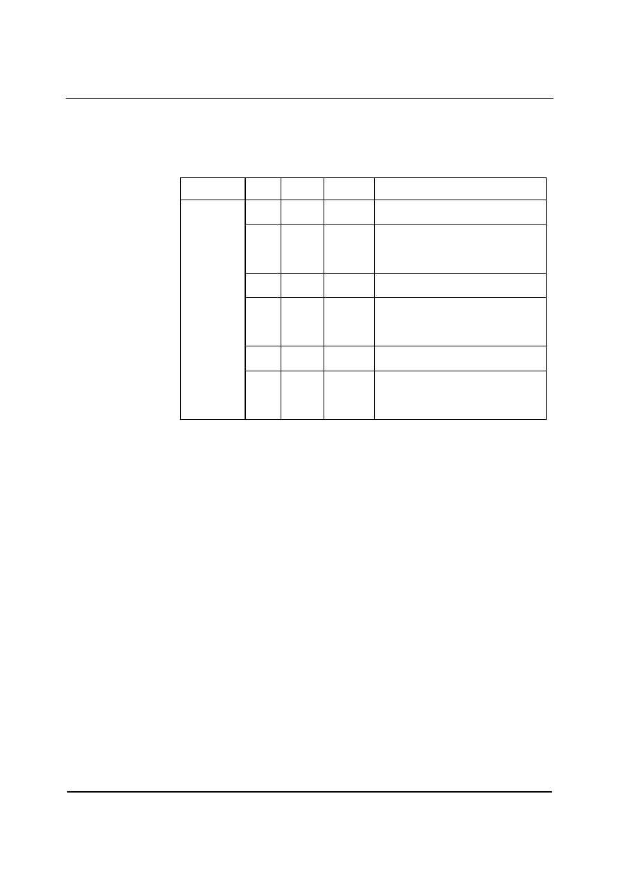
ABSOLUTE MAXIMUM RATINGS
Absolute Maximum Ratings are stress ratings only. Permanent damage to the device may be caused by continuously operating at
or beyond these limits. Device functional operating limits and guaranteed performance specifications are given under Electrical
Characteristics at the test conditions specified.
ESD Sensitive Device. This device is manufactured on a CMOS process. It is therefore generically susceptible
to damage from excessive static voltages. Proper ESD precautions must be taken during handling and storage
of this device.
Wolfson tests its package types according to IPC/JEDEC J-STD-020B for Moisture Sensitivity to determine acceptable storage
conditions prior to surface mount assembly. These levels are:
MSL1 = unlimited floor life at <30
∞
C / 85% Relative Humidity. Not normally stored in moisture barrier bag.
MSL2 = out of bag storage for 1 year at <30
∞
C / 60% Relative Humidity. Supplied in moisture barrier bag.
MSL3 = out of bag storage for 168 hours at <30
∞
C / 60% Relative Humidity. Supplied in moisture barrier bag.
The Moisture Sensitivity Level for each package type is specified in Ordering Information.
Note:
The TQFP version is classified as MSL1 and does not require to be drybagged but will be supplied as such, labelled as MSL1.
CONDITION
MIN
MAX
Digital supply voltages (DCVDD, DBVDD)
-0.3V
+3.63V
Analogue supply voltages (AVDD, HPVDD, SPKVDD, TPVDD)
-0.3V
+3.63V
Touchpanel supply voltage (TPVDD)
AVDD -0.3V
AVDD +0.3V
Voltage range digital inputs
DGND
-0.3V
DBVDD +0.3V
Voltage range analogue inputs
AGND
-0.3V
AVDD +0.3V
Voltage range touchpanel Inputs X+, X-, Y+ and Y-
TPVDD +0.3V
Voltage range touchpanel Inputs X+, X-, Y+ and Y-
AVDD +0.3V
Voltage range, BMON/AUX3 (pin31)
+5V
Operating temperature range, T
A
-25
o
C
+85
o
C
Storage temperature (TQFP package only)
-65
o
C
+150
o
C
Lead temperature (soldering 10 seconds)
+240
o
C
Lead temperature (soldering 2 minutes)
+183
o
C
RECOMMENDED OPERATING CONDITIONS
PARAMETER
SYMBOL
TEST CONDITIONS
MIN
TYP
MAX
UNIT
Digital input/output buffer
supply range
DBVDD
Notes 1, 2
1.8
3.3
3.6 or
AVDD+0.3
V
Digital core supply range
DCVDD
Notes 1, 2
1.8
3.3
3.6 or
AVDD+0.3
V
Analogue supply range
AVDD, HPVDD,
SPKVDD, TPVDD
1.8
3.3
3.6
V
Digital ground
DCGND, DBGND
0
V
Analogue ground
AGND, HPGND,
SPKGND, TPGND
0
V
Difference AGND to DGND
Note 3
-0.3
0
+0.3
V
Notes:
1.
AVDD, DCVDD and DBVDD can all be different
2.
Digital supplies (DCVDD, DBVDD) must not exceed analogue supplies (AVDD, HPVDD, SPKVDD, TPVDD) by more
than 0.3V
3.
AGND is normally the same as DGND
Production Data
WM9712L
w
PD Rev 4.0 December 2003
7
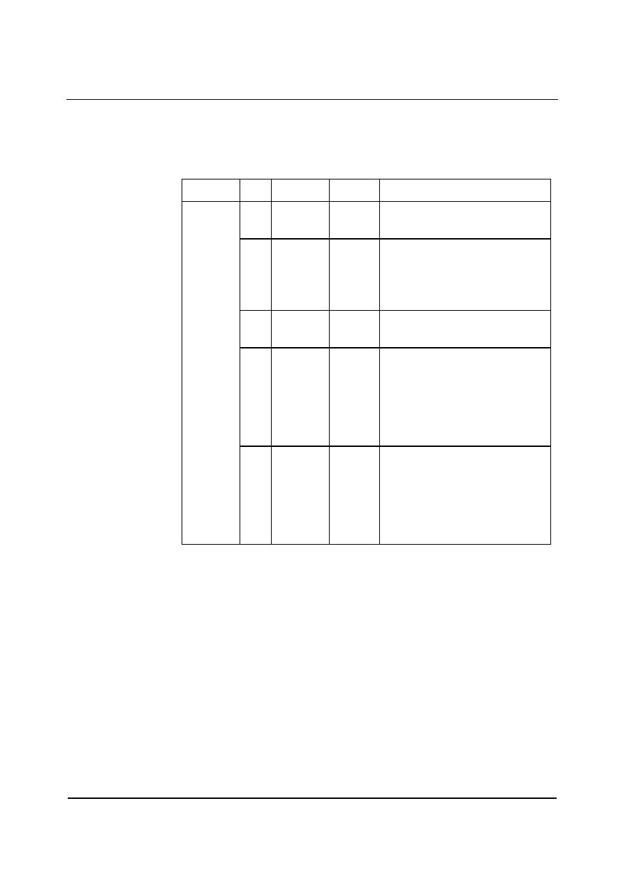
ELECTRICAL CHARACTERISTICS
AUDIO OUTPUTS
Test Conditions
DBVDD=3.3V, DCVDD = 3.3V, AVDD=HPVDD=SPKVDD =3.3V, T
A
= +25
o
C, 1kHz signal, fs = 48kHz, 18-bit audio data unless
otherwise stated.
PARAMETER
SYMBOL
TEST CONDITIONS
MIN
TYP
MAX
UNIT
DAC to Line-Out (HPOUTL/R or MONOOUT with 10k
/ 50pF load)
Full-scale output
AVDD = 3.3V, PGA gains
set to 0dB
1
V rms
Signal to Noise Ratio
(A-weighted)
SNR
85
94
dB
Total Harmonic Distortion
THD
-3dB output
-87
-80
dB
Power Supply Rejection
PSRR
100mV, 20Hz to 20kHz
signal on AVDD
50
dB
Speaker Output (LOUT2/ROUT2 with 8
bridge tied load, INV=1)
Output Power
P
O
Output power is very closely correlated with THD; see below.
P
O
=200mW
-67
0.045
Total Harmonic Distortion
THD
P
O
=400mW
-66
0.050
-60
dB
%
Signal to Noise Ratio
(A-weighted)
SNR
90
100
dB
Headphone Output (HPOUTL/R, OUT3 or LOUT2/ROUT2 with 16
or 32
load)
Output Power per channel
P
O
Output power is very closely correlated with THD; see below.
P
O
=10mW, R
L
=16
-80
P
O
=10mW, R
L
=32
-80
P
O
=20mW, R
L
=16
-79
-70
Total Harmonic Distortion
THD
P
O
=20mW, R
L
=32
-79
dB
Signal to Noise Ratio
(A-weighted)
SNR
90
95
dB
Note:
1.
All THD values are valid for the output power level quoted above ≠ for example, at HPVDD=3.3V and R
L
=16
, THD is
≠80dB when output power is 10mW. Higher output power is possible, but will result in a deterioration in THD.
WM9712L
Production Data
w
PD Rev 4.0 December 2003
8
AUDIO INPUTS
Test Conditions
DBVDD=3.3V, DCVDD = 3.3V, AVDD = 3.3V, T
A
= +25
o
C, 1kHz signal, fs = 48kHz, 18-bit audio data unless otherwise stated.
PARAMETER
SYMBOL
TEST CONDITIONS
MIN
TYP
MAX
UNIT
LINEINL/R, MICL/R and PHONE pins
AVDD = 3.3V
1.0
AVDD = 1.8V
0.545
Full Scale Input Signal Level
(for ADC 0dB Input at 0dB Gain)
V
INFS
differential input mode
(MS = 01)
half of the value listed above
V rms
0dB PGA gain
34
Input Resistance
R
IN
12dB PGA gain
10
16
22
k
Input Capacitance
5
pF
Line input to ADC (LINEINL, LINEINR, PHONE)
Signal to Noise Ratio
(A-weighted)
SNR
85
92
dB
Total Harmonic Distortion
THD
-6dBFs
-87
-80
dB
Power Supply Rejection
PSRR
20Hz to 20kHz
50
dB
Microphone input to ADC (MIC1/2 pins)
Signal to Noise Ratio
(A-weighted)
SNR
20dB boost enabled
80
dB
Total Harmonic Distortion
THD
20dB boost enabled
-80
dB
Power Supply Rejection Ratio
PSRR
50
dB
Common Mode Rejection Ratio
CMRR
Differential mic mode
TBD
dB
AUXILIARY MONO DAC (AUXDAC)
Test Conditions
AVDD = 3.3V, T
A
= +25
o
C, unless otherwise stated.
PARAMETER
SYMBOL
TEST CONDITIONS
MIN
TYP
MAX
UNIT
Resolution
12
bits
Full scale output voltage
AVDD=3.3V
1
Vrms
Signal to Noise Ratio
(A-weighted)
SNR
65
70
dB
Total Harmonic Distortion
THD
-62
-50
dB

Production Data
WM9712L
w
PD Rev 4.0 December 2003
9
TOUCHPANEL AND AUXILIARY ADC
Test Conditions
DBVDD=3.3V, DCVDD = 3.3V, AVDD = TPVDD = 3.3V, T
A
= +25
o
C, MCLK = 24.576 MHz, unless otherwise stated.
PARAMETER
SYMBOL
TEST CONDITIONS
MIN
TYP
MAX
UNIT
Input Pins X+, X-, Y+, Y-, WIPER/AUX4, COMP1/AUX1, COMP2/AUX2 and BMON/AUX3
Input Voltage
AGND
AVDD
V
Input leakage current
AUX pin not selected as
AUX ADC input
<10
nA
ADC Resolution
12
bits
Differential Non-Linearity Error
DNL
±
0.25
±
1
LSB
Integral Non-Linearity Error
INL
±
2
LSB
Offset Error
±
4
LSB
Gain Error
±
6
LSB
Power Supply Rejection
PSRR
50
dB
Throughput Rate
DEL = 1111
(zero settling time)
48
kHz
Settling Time (programmable)
MCLK = 24.576MHz
0
6
ms
Conversion Time
Note: touch pressure
measurements require
two conversions
20.8
µ
s
Switch matrix resistance
12
Programmable Pull-up resistor
R
PU
RPU = 000001
55
63
70
k
Pen down detector threshold
VDD/2
V
PIL = 1
400
Pressure measurement current
I
P
PIL = 0
200
µ
A
BMON/AUX3 (pin 31 only)
AVDD = 3.3V
AGND
5
V
Input Range
AVDD = 1.8V
AGND
3.3
V
Scaling
-3%
1/3
+3%
during measurement
30
Input Resistance (Note 1)
average over time
30 /
duty cycle
k
Note:
1. Current only flows into pin 31 during a measurement. At all other times, BMON/AUX3 is effectively an open circuit.
COMPARATORS
Test Conditions
AVDD = 3.3V, T
A
= +25
o
C, unless otherwise stated.
PARAMETER
SYMBOL
TEST CONDITIONS
MIN
TYP
MAX
UNIT
COMP1/AUX1 and COMP2/AUX2 (pins 29, 30)
Input Voltage
AGND
AVDD
V
Input leakage current
pin not selected as AUX
ADC input
<10
nA
Comparator Input Offset
(COMP1, COMP2 only)
-50
+50
mV
COMP2 delay (COMP2 only)
24.576MHz crystal
0
10.9
s
WM9712L
Production Data
w
PD Rev 4.0 December 2003
10
REFERENCE VOLTAGES
Test Conditions
DBVDD=3.3V, DCVDD = 3.3V, AVDD = 3.3V, T
A
= +25
o
C, 1kHz signal, fs = 48kHz, 18-bit audio data unless otherwise stated.
PARAMETER
SYMBOL
TEST CONDITIONS
MIN
TYP
MAX
UNIT
Audio ADCs, DACs, Mixers
Reference Input/Output
CAP2 pin
1.6
1.65
1.7
V
Buffered Reference Output
VREF pin
1.6
1.65
1.7
V
Microphone Bias
Bias Voltage
V
MICBIAS
2.88
2.97
3.06
V
Bias Current Source
I
MICBIAS
3
mA
Output Noise Voltage
Vn
1K to 20kHz
15
nV/
Hz
DIGITAL INTERFACE CHARACTERISTICS
Test Conditions
DBVDD = 3.3V, DCVDD = 3.3V, T
A
= +25
o
C, unless otherwise stated.
PARAMETER
SYMBOL
TEST CONDITIONS
MIN
TYP
MAX
UNIT
Digital Logic Levels (all digital input or output pins) ≠ CMOS Levels
Input HIGH level
DBVDD
◊
0.7
V
Input LOW level
DBVDD
◊
0.3
V
Output HIGH level
source current = 2mA
DBVDD
◊
0.9
Output LOW level
sink current = 2mA
DBVDD
◊
0.1
Clock Frequency
Master clock (XTLIN pin)
24.576
MHz
AC'97 bit clock (BIT_CLK pin)
12.288
MHz
AC'97 sync pulse (SYNC pin)
48
kHz
Note:
1.
All audio and non-audio sample rates and other timing scales proportionately with the master clock.
2.
For signal timing on the AC-Link, please refer to the AC'97 specification (Revision 2.2)

Production Data
WM9712L
w
PD Rev 4.0 December 2003
11
HEADPHONE / SPEAKER OUTPUT THD VERSUS POWER
Headphone Power vs THD+N (32Ohm load)
-100
-80
-60
-40
-20
0
5
10
15
20
25
30
Power (mW)
THD
+
N
(
d
B)
Headphone Power vs THD+N (16Ohm load)
-100
-80
-60
-40
-20
0
10
20
30
40
50
60
Power (mW)
THD+N
(
d
B)
WM9712L
Production Data
w
PD Rev 4.0 December 2003
12
POWER CONSUMPTION
The power consumption of the WM9712L depends on the following factors.
∑
Supply voltages: Reducing the supply voltages also reduces digital supply currents, and therefore results in significant
power savings especially in the digital sections of the WM9712L.
∑
Operating mode: Significant power savings can be achieved by always disabling parts of the WM9712L that are not
used (e.g. audio ADC, DAC, touchpanel digitiser).
Mode Description
26h 14:8
24h 15:0
Other Settings
Total Power
V
I (mA)
V
I (mA)
V
I (mA)
(mW)
OFF (lowest possible power)
1111111 0111111111111111 58h, SVD = 1
3.3
0.0005
3.3
0
3.3
0
0.00165
Clocks stopped
2.5
0.0004
2.5
0
2.5
0
0.001
1.8
0.0003
1.8
0
1.8
0
0.00054
LPS (Low Power Standby)
1111111 0111111111111111
3.3
0.005
3.3
0
3.3
0
0.0165
VREF maintained using 1MOhm string
2.5
0.004
2.5
0
2.5
0
0.01
1.8
0.003
1.8
0
1.8
0
0.0054
Standby Mode (ready to playback)
1110111 0111111111111111
3.3
0.56
3.3
0
3.3
0
1.848
VREF maintained using 50kOhm string
2.5
0.37
2.5
0
2.5
0
0.925
1.8
0.241
1.8
0
1.8
0
0.4338
"Idle" Mode
1100111 0111111111111111
3.3
1.1
3.3
0
3.3
0
3.63
VREF maintained using 50kOhm string
2.5
0.76
2.5
0
2.5
0
1.9
use LPS mode instead, if possible
1.8
0.508
1.8
0
1.8
0
0.9144
Touchpanel only (waiting for pen-down)
1101111 0111111111111111 76h = 0C00h
3.3
0.05
3.3
1.301
3.3
3.26
15.2163
AC-Link running
78h = 0001h
2.5
0.02
2.5
0.883
2.5
2.1
7.5075
1.8
0.009
1.8
0.571
1.8
1.41
3.582
Touchpanel only (continuous conversion)
1001111 0111111111111111 76h = 0C00h
3.3
0.08
3.3
5.85
3.3
2.67
28.38
93.75 points per second
78h = C001h
2.5
0.04
2.5
3.922
2.5
2.1
15.155
1.8
0.027
1.8
2.87
1.8
1.41
7.7526
Phone Call - using headphone / ear speaker
0110011 0111100010101100 0Eh, bit 7 = 1
3.3
2.36
3.3
0
3.3
0
7.788
HPOUTL, HPOUTR and OUT3 active
(mic gain boost)
2.5
1.838
2.5
0
2.5
0
4.595
AC-Link stopped
1.8
1.218
1.8
0
1.8
0
2.1924
Phone Call - using loudspeaker
1110011 0111101100110100 0Eh, bit 7 = 1
3.3
2.385
3.3
0
3.3
0
7.8705
AC-Link stopped
(mic gain boost)
2.5
1.837
2.5
0
2.5
0
4.5925
1.8
1.218
1.8
0
1.8
0
2.1924
Record from mono microphone
1000110 0110101111111111 0Eh, bit 7 = 1
3.3
3.27
3.3
11.21
3.3
2.6
56.364
with MICBIAS
(mic gain boost)
2.5
2.66
2.5
7.78
2.5
2.13
31.425
all analogue outputs disabled
1.8
1.838
1.8
5.21
1.8
1.41
15.2244
Record phone call
0000000 0000000010001000 0Eh, bit 7 = 1
3.3
9.461
3.3
12.22
3.3
2.62
80.1933
both sides mixed to mono
(mic gain boost)
2.5
7.46
2.5
8.552
2.5
2.1
45.28
call using headphone / ear speaker
1.8
5.318
1.8
5.799
1.8
1.48
22.6746
DAC Playback - using loudspeaker
1000001 0001111101110111
3.3
3.45
3.3
9.884
3.3
2.6
52.5822
2.5
2.549
2.5
6.755
2.5
2.1
28.51
1.8
1.738
1.8
4.606
1.8
1.41
13.9572
DAC Playback - using headphone
0000001 0001110011101111
3.3
3.62
3.3
9.8
3.3
2.6
52.866
2.5
2.71
2.5
6.78
2.5
2.1
28.975
1.8
1.748
1.8
4.606
1.8
1.47
14.0832
DAC Playback - to Line-out
0000001 0001110011110111
3.3
3.62
3.3
9.8
3.3
2.6
52.866
2.5
2.71
2.5
6.78
2.5
2.1
28.975
1.8
1.748
1.8
4.606
1.8
1.41
13.9752
Maximum Power (everything on)
0000000 0000000000000000 0Eh, bit 7 = 1
3.3
9.593
3.3
12.26
3.3
2.62
80.7609
(mic gain boost)
2.5
7.37
2.5
8.563
2.5
2.12
45.1325
1.8
5.388
1.8
5.8
1.8
1.48
22.8024
AVDD
DCVDD
DBVDD
Table 1 Supply Current Consumption
Notes:
1.
All figures are at T
A
= +25
o
C, audio sample rate fs = 48kHz, with zero signal (quiescent).
2.
The power dissipated in the headphone, speaker and touchpanel is not included in the above table.

Production Data
WM9712L
w
PD Rev 4.0 December 2003
13
DEVICE DESCRIPTION
INTRODUCTION
The WM9712L is designed to meet the mixed-signal requirements of portable and wireless computer
systems. It includes audio recording and playback, touchpanel digitisation, battery monitoring,
auxiliary ADC and GPIO functions, all controlled through a single 5-wire AC-Link interface.
SOFTWARE SUPPORT
The basic audio features of the WM9712L are software compatible with standard AC'97 device
drivers. However, to better support the touchpanel and other additional functions, Wolfson
Microelectronics supplies custom device drivers for selected CPUs and operating systems. Please
contact your local Wolfson Sales Office for more information.
AC'97 COMPATIBILITY
The WM9712L uses an AC'97 interface to communicate with a microprocessor or controller. The
audio and GPIO functions are largely compliant with AC'97 Revision 2.2. The following differences
from the AC'97 standard are noted:
∑
Pinout: The function of some pins has been changed to support device specific features.
The PHONE and PCBEEP pins have been moved to different locations on the device
package.
∑
Package: The default package for the WM9712L is a 7
◊
7mm leadless QFN package.
However, it may also be supplied in a 48-pin TQFP package, as specified in the AC'97
standard.
∑
Audio mixing: The WM9712L handles all the audio functions of a smartphone, including
audio playback, voice recording, phone calls, phone call recording, ring tones, as well as
simultaneous use of these features. The AC'97 mixer architecture does not fully support
this. The WM9712L therefore uses a modified AC'97 mixer architecture with three
separate mixers.
∑
Tone Control, Bass Boost and 3D Enhancement: These functions are implemented in
the digital domain and therefore affect only signals being played through the audio
DACs, not all output signals as stipulated in AC'97.
Some other functions are additional to AC'97:
∑
On-chip BTL loudspeaker driver
∑
On-chip BTL driver for ear speaker (phone receiver)
∑
Auxiliary mono DAC for ring tones, system alerts etc.
∑
Touchpanel controller
∑
Auxiliary ADC Inputs
∑
2 Analogue Comparators for Battery Alarm
∑
Programmable Filter Characteristics for Tone Control and 3D Enhancement
WM9712L
Production Data
w
PD Rev 4.0 December 2003
14
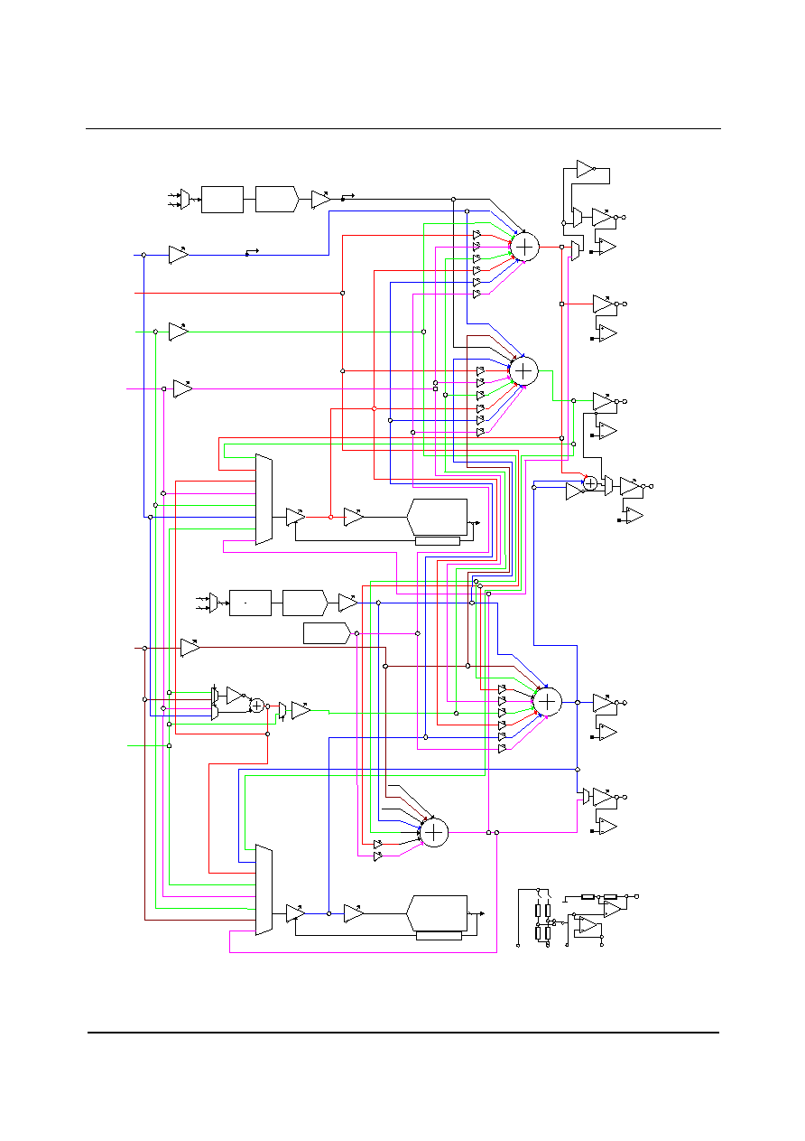
AUDIO PATHS OVERVIEW
LINEL PGA
L
LOUT2
Pin 35
MONOOUT
Pin 33
R
ROUT2
Pin 36
OUT3
Pin 37
LINER
MICR
DACR
LINER
MICR
DACR
PHONE
PCBEEP
MONOMIX
PHONE
PCBEEP
MONOMIX
MICL
MICL
ALCL
ALCR
ALCL
ALCR
Left Channel
18 Bit ADC
Variable Slot
5C:1-0 (ASS)
5C:3 (HPF)
5C:4 (ADCO)
ALC:5Ch/60h/62h
12 Bit Resistor
string DAC
2Eh/64h/12h:0(EN)
AUXDAC
AUXDAC
SPKRMIX
SPKRMIX
FROM
LINEL
PGA
FROM
DACL
to SPKR MIXER
to SPKR MIXER
Left Channel
18 Bit DAC
18h:12-8
00000 = +12dB
11111 = -34.5dB
headphone
mixer L
18
h:1
5
10
h:1
5
0Ah:1
5-12
Phone
Mixer
18
h:1
3
0Ah7:4
1A
h:
13
-1
1
10h:12-8
00000 = +12dB
11111 = -34.5dB
0Ch:0-4
00000 = +12dB
11111 = -34.5dB
0Eh:12-8
00000 = +12dB
11111 = -34.5dB
1Ah:
10-8
1Ah:14
0 = 0dB
1 = 20dB
18h:4-0
00000 = +12dB
11111 = -34.5dB
10h:5-0
00000 = +12dB
11111 = -34.5dB
0Eh:5-0
00000 = +12dB
11111 = -34.5dB
headphone
mixer R
0Ah:1
5-12
Speaker
Mixer
10
h:1
4
18
h:1
4
0Ch:14
0Ah
:11-
8
Right Channel
18 Bit ADC
Variable Slot
5C:1-0 (ASS)
5C:3 (HPF)
5C:4 (ADCO)
1Ah:
2-0
Zero-
cross
detect
02h:12-8
00000 = 0dB
11111 = -46.5dB
Zero-
cross
detect
04h:12-8
00000 = 0dB
11111 = -46.5dB
HPOUTL
Pin 39
Zero-
cross
detect
06h:4-0
00000 = 0dB
11111 = -46.5dB
Zero-
cross
detect
16h:4-0
00000 = 0dB
11111 = -46.5dB
Zero-
cross
detect
04h:4-0
00000 = 0dB
11111 = -46.5dB
HPOUTR
Pin 41
Zero-
cross
detect
02h:4-0
00000 = 0dB
11111 = -46.5dB
0dB / 20dB
OEh:6-5 (MS)
ALC:5Ch/60h/62h
0Eh:6-5
(MS)
5Ch:8 (DS)
02h:6 (INV)
02h:7 (ZC)
02h:15 (MUTE)
04h:7 (ZC)
04h:15 (MUTE)
06h:7 (ZC)
06h:15 (MUTE)
16h:7 (ZC)
16h:15 (MUTE)
04h:7 (ZC)
04h:15 (MUTE)
02h:7 (ZC)
02h:15 (MUTE)
16h:10-9
(OUT3SRC)
16h:8 (SRC)
1Ah:14
0 = 0dB
1 = 20dB
1Ch:6 (GRR=1)
1Ch:5-0
11111 = +30dB
00000 = -17.25dB
1Ch:6 (GRR=0)
1Ch:3:0
0000 = 0db
1111 = +22.5dB
1Ch:6 (GRL=1)
1Ch:13-8
11111 = +30dB
00000 = -17.25dB
1Ch:13 (GRL=0)
1Ch:11:8
0000 = 0db
1111 = +22.5dB
Slot 3
Tone and 3D
08h / 22h /
20h:13 (3DE)
Slot 4
Tone and 3D
08h / 22h /
20h:13 (3DE)
AC Link
AC Link
AC Link
PCM
PGA
PCM
PGA
ADC
PGA
ADC
PGA
PHONE PGA
MICL PGA
LINER PGA
MICR PGA
Right Channel
18 Bit DAC
L Line Volume
R Line Volume
L Headphone Volume
R Headphone Volume
Mono Volume
OUT3 Volume
500k
500k
50k
50k
PR3 (REF disable) &
58h:10 (SVD)
3.6k
4.5k
10
h:1
3
0C
h:1
5
0C
h:1
5
6dB -> -15dB
6dB -> -15dB
6dB -> -15dB
6dB -> -15dB
6dB -> -15dB
18h:1
3
18
h:1
5
18h:1
4
10
h:1
3
10
h:1
5
10
h1
4
14h:
15-1
2
0E
h:13
+7
14h:
15-1
2
14
h:1
1-7
14
h:11
-8
14
h:
11
-7
14
h:
11
-8
1A
h:
13
-1
1
12
h:
15
-1
2
12
h:
7-
4
12
h:
15
-1
2
12
h:11
-8
6dB -> -15dB
6dB -> -15dB
0dB / 20dB
6dB -> -15dB
6dB -> -15dB
6dB -> -15dB
6dB -> -15dB
0dB / 20dB
6dB -> -15dB
6dB -> -15dB
6dB -> -15dB
6dB -> -15dB
16h:8 (SRC)
1
0
1
0
1Ch:15 (Mute)
Gain Ranges:
Gain Ranges:
1Ch:15 (Mute)
14h:15-12
0Eh
:14+
7
14h:15-12
1
0
ADC Left
20h:7
(Loopback)
AC Link
1
0
ADC Right
20h:7
(Loopback)
6dB -> -15dB
0dB / 20dB
0
1
MICBIAS
Pin 28
LINEINL
Pin 23
PCBEEP
Pin 19
PHONE
Pin 20
MIC1
Pin 21
LINEINR
Pin 24
MIC2
Pin 22
AVDD
Pin 25
VREF
Pin 27
AGND
Pin 24
CAP2
Pin 32
Figure 1 Audio Paths Overview

Production Data
WM9712L
w
PD Rev 4.0 December 2003
15
AUDIO INPUTS
The following sections give an overview of the analogue audio input pins and their function. For more
information on recommended external components, please refer to the "Applications Information"
section.
LINE INPUT
The LINEINL and LINEINR inputs are designed to record line level signals, and/or to mix into one of
the analogue outputs.
Both pins are directly connected to the record selector. The record PGA adjusts the recording
volume, controlled by register 1Ch or by the ALC function.
For analogue mixing, the line input signals pass through a separate PGA, controlled by register 10h.
The signals can be routed into all three output mixers (headphone, speaker and phone). Each
LINEIN-to-mixer path has an independent mute bit. When the line inputs are not used, the line-in
PGA can be switched off to save power (see "Power Management" section).
LINEINL and LINEINR are biased internally to the reference voltage VREF. Whenever the inputs are
muted or the device placed into standby mode, the inputs remain biased to VREF using special anti-
thump circuitry to suppress any audible clicks when changing inputs.
REGISTER
ADDRESS
BIT
LABEL
DEFAULT
DESCRIPTION
12:8
LINEINL
VOL
01000
(0dB)
LINEINL input gain
00000: +12dB
... (1.5dB steps)
11111: -34.5dB
4:0
LINEINR
VOL
01000
(0dB)
LINEINR input gain
similar to LINEINLVOL
15
L2H
1
Mute LINEIN path to headphone mixer
1: Mute, 0: No mute (ON)
14
L2S
1
Mute LINEIN path to speaker mixer
1: Mute, 0: No mute (ON)
10h
13
L2P
1
Mute LINEIN path to phone mixer
1: Mute, 0: No mute (ON)
Table 2 Line Input Control
MICROPHONE INPUT
The MIC1 and MIC2 inputs are designed for direct connection to single-ended mono, stereo or
differential mono microphone. If the microphone is mono, the same signal appears on both left and
right channels. In stereo mode, MIC1 is routed to the left and MIC2 to the right channel.
For voice recording, the microphone signal is directly connected to the record selector. The record
PGA adjusts the recording volume, controlled by register 1Ch or by the ALC function.
For analogue mixing, the signal passes through a separate PGA, controlled by register 0Eh. The
microphone signal can be routed into the phone mixer (for normal phone call operation) and/or the
headphone mixer (using register 14h, see "Audio Mixers / Sidetone Control" section), but not into the
speaker mixer (to prevent acoustic feedback from the speaker into the microphone). When the
microphone inputs are not used, the microphone PGA can be switched off to save power (see
"Power Management" section).
MIC1 and MIC2 are biased internally to the reference voltage VREF. Whenever the inputs are muted
or the device placed into standby mode, the inputs remain biased to VREF using special anti-thump
circuitry to suppress any audible clicks when changing inputs.
WM9712L
Production Data
w
PD Rev 4.0 December 2003
16
It is also possible to use the LINEINL and LINEINR pins as a second differential microphone input.
This is achieved by setting the DS bit (register 5Ch, bit 11) to `1'. This disables the line-in audio paths
and routes the signal from LINEINL and LINEINR through the differential mic path, as if it came from
the MIC1 and MIC2 pins. Only one differential microphone be used at a time. The DS bit only has an
effect when MS = 01 (differential mode).
REGISTER
ADDRESS
BIT
LABEL
DEFAULT
DESCRIPTION
14
M12P
1
Mute MIC1 path to phone mixer
1: Mute, 0: No mute (ON)
13
M22P
1
Mute MIC2 path to phone mixer
1: Mute, 0: No mute (ON)
12:8
LMICVOL
01000
(0dB)
Left microphone volume
Only used when MS = 11
Similar to MICVOL
7
20dB
0
Microphone gain boost (Note 1)
1: 20dB boost ON
0: No boost (0dB gain)
Microphone mode select
00
Single-ended mono (left)
left = right = MIC1 (pin 21)
Volume controlled by MICVOL
01
Differential mono mode
left = right = MIC1 ≠ MIC2
Volume controlled by MICVOL
10
Single-ended mono (right)
left = right = MIC2 (pin 22)
Volume controlled by MICVOL
6:5
MS
00
11
Stereo mode
MIC1 = left, MIC2 = right
Left Volume controlled by LMICVOL
Right volume controlled by MICVOL
0Eh
Mic Volume
4:0
MICVOL
01000
(0dB)
Microphone volume to mixers
00000: +12dB
... (1.5dB steps)
11111: -34.5dB
5Ch
Additional
Analogue
Functions
8
DS
0
Differential Microphone Select
0 : Use MIC1 and MIC2
1: Use LINEL and LINER
Table 3 Microphone Input Control
Note:
1.
The 20dB gain boost acts on the input to the phone mixer only. A separate microphone
boost for recording can be enabled using the BOOST bit in register 1Ah.
MICROPHONE BIAS
The MICBIAS output (pin 28) provides a low noise reference voltage suitable for biasing electret type
microphones and the associated external resistor biasing network. The internal MICBIAS circuitry is
shown below. Note that the maximum source current capability for MICBIAS is 3mA. The external
biasing resistors and microphone cartridge therefore must limit the MICBIAS current to 3mA.

Production Data
WM9712L
w
PD Rev 4.0 December 2003
17
AGND
MICBIAS
= 1.8 x CAP2
= 0.9 X AVDD
CAP2
WM9712L
Figure 2 Microphone Bias Schematic
PHONE INPUT
Pin 20 (PHONE) is a mono, line level input designed to connect to the receive path of a telephony
device.
The pin connects directly to the record selector for phone call recording (Note: to record both sides of
a phone call, one ADC channel should record the PHONE signal while the other channel records the
MIC signal). The RECVOL PGA adjusts the recording volume, controlled by register 1Ch or by the
ALC function.
To listen to the PHONE signal, the signal passes through a separate PGA, controlled by register
0Ch. The signal can be routed into the headphone mixer (for normal phone call operation) and/or the
speaker mixer (for speakerphone operation), but not into the phone mixer (to prevent forming a
feedback loop). When the phone input is not used, the phone-in PGA can be switched off to save
power (see "Power Management" section).
PHONE is biased internally to the reference voltage VREF. Whenever the input is muted or the
device placed into standby mode, the input remains biased to VREF using special anti-thump
circuitry to suppress any audible clicks when changing inputs.
REGISTER
ADDRESS
BIT
LABEL
DEFAULT
DESCRIPTION
15
P2H
1
Mute PHONE path to headphone mixer
1: Mute, 0: No mute (ON)
14
P2S
1
Mute PHONE path to speaker mixer
1: Mute, 0: No mute (ON)
0Ch
Phone Input
4:0
PHONE
VOL
01000
(0dB)
PHONE input gain
00000: +12dB
... (1.5dB steps)
11111: -34.5dB
Table 4 Phone Input Control
WM9712L
Production Data
w
PD Rev 4.0 December 2003
18
PCBEEP INPUT
Pin 19 (PCBEEP) is a mono, line level input intended for externally generated signal or warning
tones. It is routed directly to the record selector and all three output mixers, without an input
amplifier. The signal gain into each mixer can be independently controlled, with a separate mute bit
for each signal path.
REGISTER
ADDRESS
BIT
LABEL
DEFAULT
DESCRIPTION
15
B2H
1
Mute PCBEEP path to headphone mixer
1: Mute, 0: No mute (ON)
14:12
B2HVOL
010
(0dB)
PCBEEP to headphone mixer gain
000: +6dB
... (3dB steps)
111: -15dB
11
B2S
1
Mute PCBEEP path to speaker mixer
1: Mute, 0: No mute (ON)
10:8
B2SVOL
010
(0dB)
PCBEEP to speaker mixer gain
000: +6dB
... (3dB steps)
111: -15dB
7
B2P
1
Mute PCBEEP path to phone mixer
1: Mute, 0: No mute (ON)
0Ah
PCBEEP input
6:4
B2PVOL
010
(0dB)
PCBEEP to phone mixer gain
000: +6dB
... (3dB steps)
111: -15dB
Table 5 PCBEEP Control

Production Data
WM9712L
w
PD Rev 4.0 December 2003
19
AUDIO ADC
The WM9712L has a stereo sigma-delta ADC to digitize audio signals. The ADC achieves high
quality audio recording at low power consumption. The ADC sample rate can be controlled by writing
to a control register (see "Variable Rate Audio"). It is independent of the DAC sample rate.
To save power, the left and right ADCs can be separately switched off using the PD11 and PD12
bits, whereas PR0 disables both ADCs (see "Power Management" section). If only one ADC is
running, the same ADC data appears on both the left and right AC-Link slots.
HIGH PASS FILTER
The WM9712L audio ADC incorporates a digital high-pass filter that eliminates any DC bias from the
ADC output data. The filter is enabled by default. For DC measurements, it can be disabled by
writing a `1' to the HPF bit (register 5Ch, bit 3).
ADC SLOT MAPPING
By default, the output of the left audio ADC appears on slot 3 of the SDATAIN signal (pin 8), and the
right ADC data appears on slot 4. However, the ADC output data can also be sent to other slots, by
setting the ASS (ADC slot select) control bits as shown below.
REGISTER
ADDRESS
BIT
LABEL
DEFAULT
DESCRIPTION
1:0
ASS
00
ADC to slot mapping
00: Left = Slot 3, Right = Slot 4 (default)
01: Left = Slot 7, Right = Slot 8
10: Left = Slot 6, Right = Slot 9
11: Left = Slot 10, Right = Slot 11
5Ch
Additional
Function
Control
3
HPF
0
High-pass filter disable
0: Filter enabled (for audio)
1: Filter disabled (for DC measurements)
Table 6 ADC Control
WM9712L
Production Data
w
PD Rev 4.0 December 2003
20
RECORD SELECTOR
The record selector determines which input signals are routed into the audio ADC. The left and right
channels can be selected independently. This is useful for recording a phone call: one channel can
be used for the RX signal and the other for the TX signal, so that both sides of the conversation are
digitized.
REGISTER
ADDRESS
BIT
LABEL
DEFAULT
DESCRIPTION
14
BOOST
0
20dB Boost
1: Boost ADC input signal by 20dB
0 :No boost
13:12
R2P
11
Record to phone path enable
00: Left ADC and Right ADC to phone
mixer
01 : Left ADC to phone mixer
10: Right ADC to phone imixer
11 : Muted
11
R2PBOOST
0
20dB Boost for ADC to phone signal
1: Boost signal by 20dB
0 :No boost
10:8
RECSL
000
Left ADC signal source
000: MIC* (pre-PGA)
001-010: Reserved (do not use this setting)
011: Speaker mix
100: LINEINL (pre-PGA)
101: Headphone Mix (left)
110: Phone Mix
111: PHONE (pre-PGA)
1Ah
Record
Select
2:0
RECSR
000
Right ADC signal source
000: MIC* (pre-PGA)
001-010: Reserved (do not use this setting)
011: Speaker mix
100: LINEINR (pre-PGA)
101: Headphone Mix (right)
110: Phone Mix
111: PHONE (pre-PGA)
Table 7 Audio Record Selector
Note:
*In stereo mic mode, MIC1 is routed to the left ADC and MIC2 to the right ADC. In all mono
mic modes, the same signal (MIC1, MIC2 or MIC1-MIC2) is routed to both the left and right
ADCs. See "Microphone Input" section for details.
Production Data
WM9712L
w
PD Rev 4.0 December 2003
21
RECORD GAIN
The amplitude of the signal that enters the audio ADC is controlled by the Record PGA
(Programmable Gain Amplifier). The PGA gain can be programmed either by writing to the Record
Gain register, or by the Automatic Level Control (ALC) circuit (see next section). When the ALC is
enabled, any writes to the Record Gain register have no effect.
Two different gain ranges can be implemented: the standard gain range defined in the AC'97
standard, or an extended gain range with smaller gain steps. The ALC circuit always uses the
extended gain range, as this has been found to result in better sound quality.
The output of the Record PGA can also be mixed into the phone and/or headphone outputs (see
"Audio Mixers"). This makes it possible to use the ALC function for the microphone signal in a
smartphone application.
REGISTER
ADDRESS
BIT
LABEL
DEFAULT
DESCRIPTION
15
RMU
1
Mute Audio ADC (both channels)
1: Mute (OFF)
0: No Mute (ON)
14
GRL
0
Gain range select (left)
0: Standard (0 to 22.5dB, 1.5dB step size)
1: Extended (-17.25 to +30dB, 0.75dB steps)
Record Volume (left)
Standard (GRL=0)
Extended (GRL=1)
13:8
RECVOLL
000000
XX0000: 0dB
XX0001: +1.5dB
... (1.5dB steps)
XX1111: +22.5dB
000000: -17.25dB
000001: -16.5dB
... (0.75dB steps)
111111: +30dB
7
ZC
0
Zero Cross Enable
0: Record Gain changes immediately
1: Record Gain changes when signal is zero
or after time-out
6
GRR
0
Gain range select (right)
Similar to GRL
1Ch
Record Gain
5:0
RECVOLR
000000
Record Volume (right)
Similar to RECVOLL
Table 8 Record Gain Register
WM9712L
Production Data
w
PD Rev 4.0 December 2003
22
AUTOMATIC LEVEL CONTROL
The WM9712L has an automatic level control that aims to keep a constant recording volume
irrespective of the input signal level. This is achieved by continuously adjusting the PGA gain so that
the signal level at the ADC input remains constant. A digital peak detector monitors the ADC output
and changes the PGA gain if necessary.
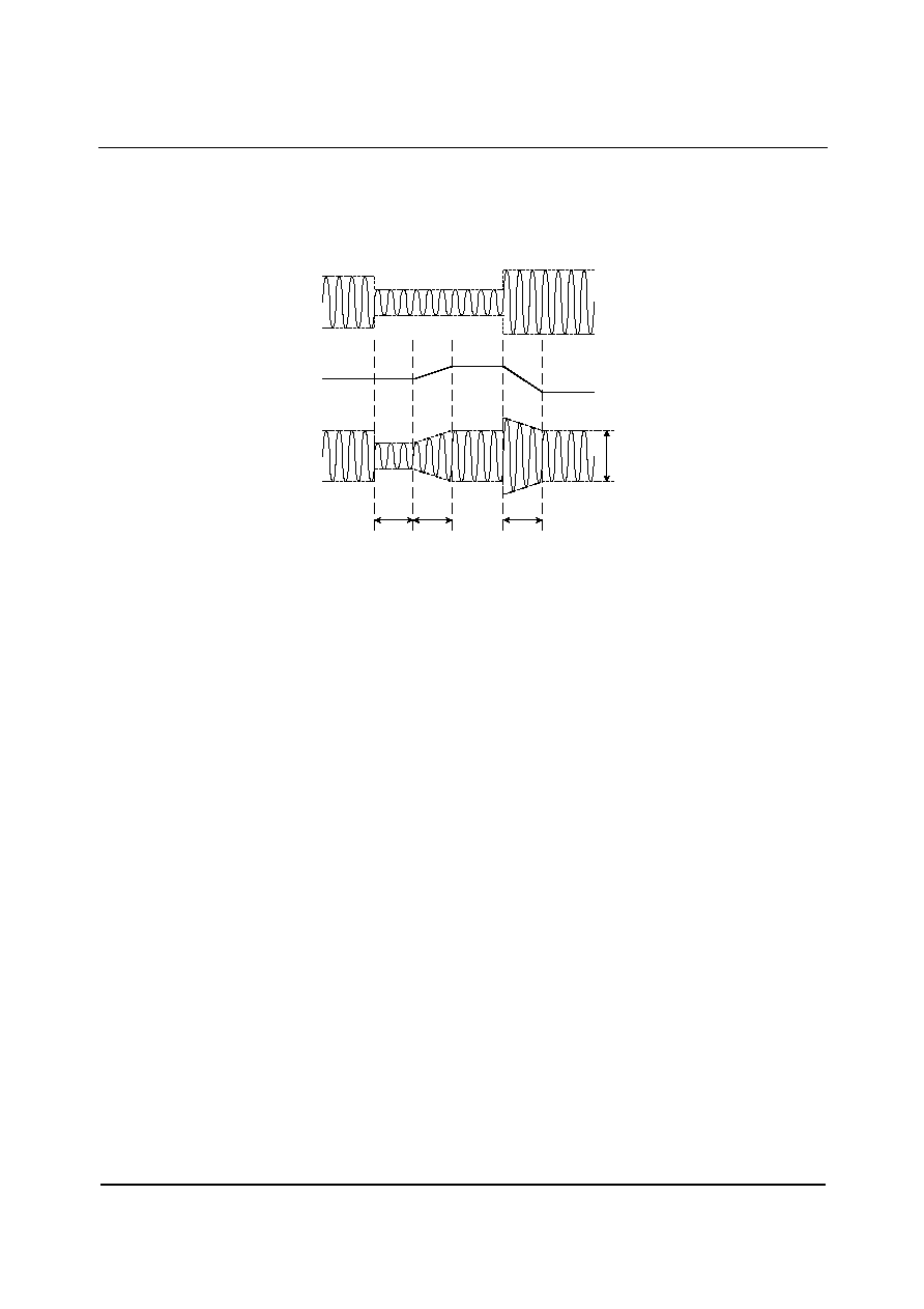
hold
time
decay
time
attack
time
input
signal
signal
after
ALC
PGA
gain
ALC
target
level
Figure 3 ALC Operation
The ALC function is enabled using the ALCSEL control bits. When enabled, the recording volume
can be programmed between ≠6dB and ≠28.5dB (relative to ADC full scale) using the ALCL register
bits.
HLD, DCY and ATK control the hold, decay and attack times, respectively:
Hold time is the time delay between the peak level detected being below target and the PGA gain
beginning to ramp up. It can be programmed in power-of-two (2
n
) steps, e.g. 2.67ms, 5.33ms,
10.67ms etc. up to 43.7s. Alternatively, the hold time can also be set to zero. The hold time only
applies to gain ramp-up, there is no delay before ramping the gain down when the signal level is
above target.
Decay (Gain Ramp-Up) Time is the time that it takes for the PGA gain to ramp up across 90% of its
range (e.g. from ≠15B up to 27.75dB). The time it takes for the recording level to return to its target
value therefore depends on both the decay time and on the gain adjustment required. If the gain
adjustment is small, it will be shorter than the decay time. The decay time can be programmed in
power-of-two (2
n
) steps, from 24ms, 48ms, 96ms, etc. to 24.58s.
Attack (Gain Ramp-Down) Time is the time that it takes for the PGA gain to ramp down across 90%
of its range (e.g. from 27.75dB down to ≠15B gain). The time it takes for the recording level to return
to its target value therefore depends on both the attack time and on the gain adjustment required. If
the gain adjustment is small, it will be shorter than the attack time. The attack time can be
programmed in power-of-two (2
n
) steps, from 6ms, 12ms, 24ms, etc. to 6.14s.
When operating in stereo, the peak detector takes the maximum of left and right channel peak
values, and any new gain setting is applied to both left and right PGAs, so that the stereo image is
preserved. However, the ALC function can also be enabled on one channel only. In this case, only
one PGA is controlled by the ALC mechanism, while the other channel runs independently with its
PGA gain set through the control register.

Production Data
WM9712L
w
PD Rev 4.0 December 2003
23
REGISTER
ADDRESS
BIT
LABEL
DEFAULT
DESCRIPTION
15:14
ALCSEL
00
(OFF)
ALC function select
00 = ALC off (PGA gain set by register)
01 = Right channel only
10 = Left channel only
11 = Stereo (PGA registers unused)
Note: Ensure that RECVOLL and RECVOLR
settings (reg. 1Ch) are the same before
entering this mode
13:11
MAXGAIN
111
(+30dB)
PGA gain limit for ALC
111 = +30dB
110 = +24dB
....(6dB steps)
001 = -6dB
000 = -12dB
8
ALCZC
0
ALC Zero Cross enable (overrides ZC bit in
register 1Ch)
0: PGA Gain changes immediately
1: PGA Gain changes when signal is zero or
after time-out
62h
ALC / Noise
Gate Control
9:10
ZC
TIMEOUT
11
Programmable zero cross timeout
11 2
17
x MCLK period
10 2
16
x MCLK period
01 2
15
x MCLK period
00 2
14
x MCLK period
15:12
ALCL
1011
(-12dB)
ALC target ≠ sets signal level at ADC input
0000 = -28.5dB FS
0001 = -27.0dB FS
... (1.5dB steps)
1110 = -7.5dB FS
1111 = -6dB FS
11:8
HLD
0000
(0ms)
ALC hold time before gain is increased.
0000 = 0ms
0001 = 2.67ms
0010 = 5.33ms
... (time doubles with every step)
1111 = 43.691s
7:4
DCY
0011
(192ms)
ALC decay (gain ramp-up) time
0000 = 24ms
0001 = 48ms
0010 = 96ms
... (time doubles with every step)
1010 or higher = 24.58s
60h
ALC Control
3:0
ATK
0010
(24ms)
ALC attack (gain ramp-down) time
0000 = 6ms
0001 = 12ms
0010 = 24ms
... (time doubles with every step)
1010 or higher = 6.14s
Table 9 ALC Control

WM9712L
Production Data
w
PD Rev 4.0 December 2003
24
MAXIMUM GAIN
The MAXGAIN register sets the maximum gain value that the PGA can be set to whilst under the
control of the ALC. This has no effect on the PGA when ALC is not enabled.
PEAK LIMITER
To prevent clipping when a large signal occurs just after a period of quiet, the ALC circuit includes a
limiter function. If the ADC input signal exceeds 87.5% of full scale (≠1.16dB), the PGA gain is
ramped down at the maximum attack rate (as when ATK = 0000), until the signal level falls below
87.5% of full scale. This function is automatically enabled whenever the ALC is enabled.
(Note: If ATK = 0000, then the limiter makes no difference to the operation of the ALC. It is designed
to prevent clipping when long attack times are used).
NOISE GATE
When the signal is very quiet and consists mainly of noise, the ALC function may cause "noise
pumping", i.e. loud hissing noise during silence periods. The WM9712L has a noise gate function
that prevents noise pumping by comparing the signal level at the input pins (i.e. before the record
PGA) against a noise gate threshold, NGTH. Provided that the noise gate function is enabled (NGAT
= 1), the noise gate cuts in when:
∑
Signal level at ADC [dB] < NGTH [dB] + PGA gain [dB] + Mic Boost gain [dB]
This is equivalent to:
∑
Signal level at input pin [dB] < NGTH [dB]
The PGA gain is then held constant (preventing it from ramping up as it normally would when the
signal is quiet). If the NGG bit is set, the ADC output is also muted when the noise gate cuts in.
The table below summarises the noise gate control register. The NGTH control bits set the noise
gate threshold with respect to the ADC full-scale range. The threshold is adjusted in 1.5dB steps.
Levels at the extremes of the range may cause inappropriate operation, so care should be taken with
set≠up of the function. Note that the noise gate only works in conjunction with the ALC function, and
always operates on the same channel(s) as the ALC (left, right, both, or none).
REGISTER
ADDRESS
BIT
LABEL
DEFAULT
DESCRIPTION
7
NGAT
0
Noise gate function enable
1 = enable
0 = disable
5
NGG
0
Noise gate type
0 = PGA gain held constant
1 = mute ADC output
62h
ALC / Noise
Gate Control
4:0
NGTH(4:0)
00000
Noise gate threshold
00000: -76.5dBFS
00001: -75dBFS
... 1.5 dB steps
11110: -31.5dBFS
11111: -30dBFS
Table 10 Noise Gate Control
Production Data
WM9712L
w
PD Rev 4.0 December 2003
25
AUDIO DACS
STEREO DAC
The WM9712L has a stereo sigma-delta DAC that achieves high quality audio playback at low power
consumption. Digital tone control, adaptive bass boost and 3-D enhancement functions operate on
the digital audio data before it is passed to the stereo DAC. (Contrary to the AC'97 specification, they
have no effect on analogue input signals or signals played through the auxiliary DAC. Nevertheless,
the ID2 and ID5 bits in the reset register, 00h, are set to `1' to indicate that the WM9712L supports
tone control and bass boost.)
The DAC output has a PGA for volume control. The DAC sample rate can be controlled by writing to
a control register (see "Variable Rate Audio"). It is independent of the ADC sample rate. The left and
right DACs can be separately powered down using the PD13 and PD14 control bits, whereas the
PR1 bit disables both DACs (see "Power Management" section).
STEREO DAC VOLUME
The volume of the DAC output signal is controlled by a PGA (Programmable Gain Amplifier). It can
be mixed into the headphone, speaker and phone output paths (see "Audio Mixers").
REGISTER
ADDRESS
BIT
LABEL
DEFAULT
DESCRIPTION
15
D2H
1
Mute DAC path to headphone mixer
1: Mute, 0: No mute (ON)
14
D2S
1
Mute DAC path to speaker mixer
1: Mute, 0: No mute (ON)
13
D2P
1
Mute DAC path to phone mixer
1: Mute, 0: No mute (ON)
12:8
DACL
VOL
01000
(0dB)
Left DAC Volume
00000: +12dB
... (1.5dB steps)
11111: -34.5dB
18h
DAC
Volume
4:0
DACR
VOL
01000
(0dB)
Right DAC Volume
similar to DACLVOL
15
AMUTE
0
Read-only bit to indicate auto-muting
1: DAC auto-muted
0: DAC not muted
5Ch
Additional
Functions
(1)
7
AMEN
0
DAC Auto-Mute Enable
1: Automatically mutes analogue output of
stereo DAC if digital input is zero
0: Auto-mute OFF
Table 11 Stereo DAC Volume Control
WM9712L
Production Data
w
PD Rev 4.0 December 2003
26
TONE CONTROL / BASS BOOST
The WM9712L provides separate controls for bass and treble with programmable gains and filter
characteristics. This function operates on digital audio data before it is passed to the audio DACs.
Bass control can take two different forms:
∑
Linear bass control: bass signals are amplified or attenuated by a user programmable
gain. This is independent of signal volume, and very high bass gains on loud signals
may lead to signal clipping.
∑
Adaptive bass boost: The bass volume is amplified by a variable gain. When the bass
volume is low, it is boosted more than when the bass volume is high. This method is
recommended because it prevents clipping, and usually sounds more pleasant to the
human ear.
Treble control applies a user programmable gain, without any adaptive boost function.
Treble, linear bass and 3D enhancement can all produce signals that exceed full-scale. In order to
avoid limiting under these conditions, it is recommended to set the DAT bit to attenuate the digital
input signal by 6dB. The gain at the outputs should be increased by 6dB to compensate for the
attenuation. Cut-only tone adjustment and adaptive bass boost cannot produce signals above full-
scale and therefore do not require the DAT bit to be set.
REGISTER
ADDRESS
BIT
LABEL
DEFAULT
DESCRIPTION
15
BB
0
Bass Mode
0 = Linear bass control
1 = Adaptive bass boost
12
BC
0
Bass Cut-off Frequency
0 = Low (130Hz at 48kHz sampling)
1 = High (200Hz at 48kHz sampling)
Bass Intensity
Code
BB=0
BB=1
0000
+9dB
15 (max)
0001
+9dB
14
0010
+7.5dB
13
...
(1.5dB steps)
...
0111
0dB
8
...
(1.5dB steps)
...
1011-1101
-6dB
4-2
1110
-6dB
1 (min)
11:8
BASS
1111
(OFF)
1111
Bypass (OFF)
6
DAT
0
-6dB attenuation
0 = Off
1 = On
4
TC
0
Treble Cut-off Frequency
0 = High (8kHz at 48kHz sampling)
1 = Low (4kHz at 48kHz sampling)
08h
DAC Tone
Control
3:0
TRBL
1111
(Disabled)
Treble Intensity
0000 or 0001 = +9dB
0010 = +7.5dB
... (1.5dB steps)
1011 to 1110 = -6dB
1111 = Treble Control Disabled
Table 12 DAC Tone Control
Note:
1.
All cut-off frequencies change proportionally with the DAC sample rate.

Production Data
WM9712L
w
PD Rev 4.0 December 2003
27
3D STEREO ENHANCEMENT
The 3D stereo enhancement function artificially increases the separation between the left and right
channels by amplifying the (L-R) difference signal in the frequency range where the human ear is
sensitive to directionality. The programmable 3D depth setting controls the degree of stereo
expansion introduced by the function. Additionally, the upper and lower limits of the frequency range
used for 3D enhancement can be selected using the 3DFILT control bits.
REGISTER
ADDRESS
BIT
LABEL
DEFAULT
DESCRIPTION
20h
General
Purpose
13
3DE
0
(disabled)
3D enhancement enable
5
3DLC
0
Lower Cut-off Frequency
0 = Low (200Hz at 48kHz sampling)
1 = High (500Hz at 48kHz sampling)
4
3DUC
0
Upper Cut-off Frequency
0 = High (2.2kHz at 48kHz sampling)
1 = Low (1.5kHz at 48kHz sampling)
22h
DAC 3D
Control
3:0
3DDEPTH
0000
3D Depth
0000: 0% (minimum 3D effect)
0001: 6.67%
...
1110: 93.3%
1111: 100% (maximum)
Table 13 Stereo Enhancement Control
Note:
1.
All cut-off frequencies change proportionally with the DAC sample rate.
WM9712L
Production Data
w
PD Rev 4.0 December 2003
28
AUXILIARY DAC
AUXDAC is a simple 12-bit mono DAC. It can be used to generate DC signals (with the numeric input
written into a control register), or AC signals such as telephone-quality ring tones or system beeps
(with the input signal supplied through an AC-Link slot). In AC mode (XSLE = 1), the input data is
binary offset coded; in DC mode (XSLE = 0), there is no offset.
The analogue output of AUXDAC is routed directly into the output mixers. The signal gain into each
mixer can be adjusted at the mixer inputs using control register 12h. In slot mode (XSLE = 1), the
AUXDAC also supports variable sample rates (See "Variable Rate Audio" section).
When the auxiliary DAC is not used, it can be powered down by setting AXE = 0. This is also the
default setting.
REGISTER
ADDRESS
BIT
LABEL
DEFAULT
DESCRIPTION
15
XSLE
0
AUXDAC input selection
0: from AUXDACVAL (for DC signals)
1: from AC-Link slot selected by
AUXDACSLT (for AC signals)
14:12
AUXDAC
SLT
000
AUXDAC Input Selection
000 ≠ Slot 5, bits 8-19 (with XSLE=1)
001 ≠ Slot 6, bits 8-19 (with XSLE=1)
010 ≠ Slot 7, bits 8-19 (with XSLE=1)
011 ≠ Slot 8, bits 8-19 (with XSLE=1)
100 ≠ Slot 9, bits 8-19 (with XSLE=1)
101 ≠ Slot 10, bits 8-19 (with XSLE=1)
110 ≠ Slot 11, bits 8-19 (with XSLE=1)
111 ≠ RESERVED (do not use)
64h
AUDAC Input
Control
11:0
AUXDAC
VAL
000h
AUXDAC Digital Input (with XSLE=0)
000h: minimum
FFFh: full-scale
15
A2H
1
Mute AUXDAC path to headphone
mixer
1: Mute, 0: No mute (ON)
14:12
A2HVOL
010
(0dB)
AUXDAC to headphone mixer gain
000: +6dB
... (3dB steps)
111: -15dB
11
A2S
1
Mute AUXDAC path to speaker mixer
1: Mute, 0: No mute (ON)
10:8
A2SVOL
010
(0dB)
AUXDAC to speaker mixer gain
000: +6dB
... (3dB steps)
111: -15dB
7
A2P
1
Mute AUXDAC path to phone mixer
1: Mute, 0: No mute (ON)
6:4
A2PVOL
010
(0dB)
AUXDAC to phone mixer gain
000: +6dB
... (3dB steps)
111: -15dB
12h
AUXDAC Output
Control
0
AXE
0
0: AUXDAC off
1: AUXDAC enabled
Table 14 AUXDAC Control

Production Data
WM9712L
w
PD Rev 4.0 December 2003
29
ANALOGUE AUDIO OUTPUTS
The following sections give an overview of the analogue audio output pins. For more information on
recommended external components, please refer to the "Applications Information" section.
HEADPHONE OUTPUTS ≠ HPOUTL AND HPOUTR
The HPOUTL and HPOUTR (pins 39 and 41) are designed to drive a 16
or 32
headphone or a
line output. They can also be used as line-out pins. The output signal is produced by the headphone
mixer.
The signal volume on HPOUTL and HPOUTR can be independently adjusted under software control
by writing to register 04h. When HPOUTL and HPOUTR are not used, the output drivers can be
disabled to save power (see "Power Management" section). Both pins remain at the same DC level
(the reference voltage VREF) when they are disabled, so that no click noise is produced.
REGISTER
ADDRESS
BIT
LABEL
DEFAULT
DESCRIPTION
15
MUTE
1
Mute HPOUTL and HPOUTR
1: Mute (OFF)
0: No Mute (ON)
13:8
HPOUTLVOL
000000
(0dB)
HPOUTL Volume
000000: 0dB (maximum)
000001: -1.5dB
... (1.5dB steps)
011111: -46.5dB
1xxxxx: -46.5dB
7
ZC
0
Zero Cross Enable
0: Change gain immediately
1: Change gain only on zero crossings,
or after time-out
04h
HPOUTL /
HPOUTR
Volume
5:0
HPOUTRVOL
00000
(0dB)
HPOUTR Volume
Similar to HPOUTLVOL
Table 15 HPOUTL / HPOUTR Control
WM9712L
Production Data
w
PD Rev 4.0 December 2003
30
EAR SPEAKER OUTPUT ≠ OUT3
Pin 37 (OUT3) has a buffer that can drive load impedances down to 16
. It can be used to:
∑
Drive an ear speaker (phone receiver). The speaker can be connected differentially
between OUT3 and HPOUTL, or in single-ended configuration (OUT3 to HPGND). The
ear speaker output is produced by the headphone mixer. The right signal must be
inverted (OUT3INV = 1), so that the left and right channel are mixed to mono in the
speaker [L≠(-R) = L+R].
∑
Eliminate the DC blocking capacitors on HPOUTL and HPOUTR. In this configuration,
OUT3 produces a buffered midrail voltage (AVDD/2) and is connected to the headphone
socket's ground pin (see "Applications Information")
∑
Produce the inverse of the MONOOUT signal, for a differential mono output.
Note: OUT3 can only handle one of the above functions at any given time.
REGISTER
ADDRESS
BIT
LABEL
DEFAULT
DESCRIPTION
15
MUTE
1
Mute OUT3
1: Mute (Buffer OFF)
0: No Mute (Buffer ON)
Source of OUT3 signal
00
inverse of HPOUTR
(for BTL ear speaker)
01
VREF (for capless headphone drive)
10
mono mix of both headphone channels
(for single-ended ear speaker)
10:9
OUT3
SRC
00
11
inverse of MONOOUT
(for differential mono output)
7
ZC
0
Zero Cross Enable
0: Change gain immediately
1: Change gain only on zero crossings, or after
time-out
16h
OUT3
Control
5:0
OUT3
VOL
000000
(0dB)
OUT3 Volume
000000: 0dB (maximum)
000001: -1.5dB
... (1.5dB steps)
011111: -46.5dB
1xxxxx: -46.5dB
Table 16 OUT3 Control

Production Data
WM9712L
w
PD Rev 4.0 December 2003
31
LOUDSPEAKER OUTPUTS ≠ LOUT2 AND ROUT2
The LOUT2 and ROUT2 outputs are designed to differentially drive an 8
mono speaker. They can
also be used as a stereo line-out or headphone output.
For speaker drive, the LOUT2 signal must be inverted (INV = 1), so that the left and right channel are
added up in the speaker [R≠(-L) = R+L].
REGISTER
ADDRESS
BIT
LABEL
DEFAULT
DESCRIPTION
15
MUTE
1
Mute LOUT2 and ROUT2
1: Mute (OFF)
0: No Mute (ON)
13:8
LOUT2VOL
00000
(0dB)
LOUT2 Volume
000000: 0dB (maximum)
000001: -1.5dB
... (1.5dB steps)
011111: -46.5dB
1xxxxx: -46.5dB
7
ZC
0
Zero Cross Enable
0: Change gain immediately
1: Change gain only on zero crossings,
or after time-out
6
INV
0
LOUT2 Invert
0 = No Inversion (0
∞
phase shift)
1 = Signal inverted (180
∞
phase shift)
02h
LOUT2/ROUT2
Volume
5:0
ROUT2VOL
00000
(0dB)
ROUT2 Volume
Similar to LOUT2VOL
16h
8
SRC
0
Source of LOUT2/ROUT2 signals
0: speaker mixer (for BTL speaker)
1: headphone mixer (for stereo output)
Table 17 LOUT2 / ROUT2 Control
Note:
1.
For BTL speaker drive, it is recommended that LOUT2VOL = ROUT2VOL.
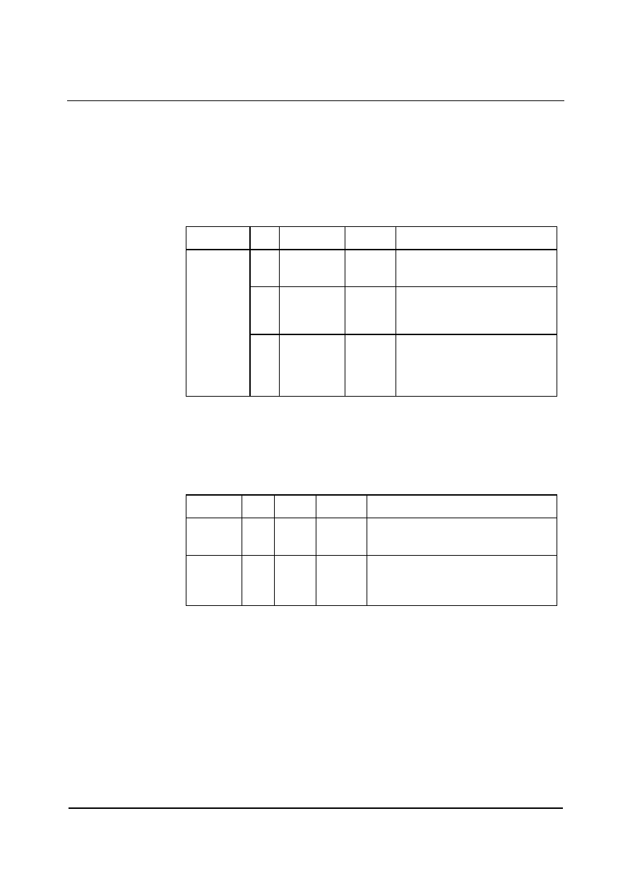
WM9712L
Production Data
w
PD Rev 4.0 December 2003
32
PHONE OUTPUT (MONOOUT)
The MONOOUT output (pin 33) is intended for connection to the TX side of a wireless chipset. The
signal is generated in a dedicated mono mixer; it is not necessarily a mono mix of the stereo outputs
HPOUTL/R or LOUT2/ROUT2 (see "Audio Mixers" section).
The MONOOUT volume can be controlled by writing to register 06h. When MONOOUT is not used,
the output buffer can be disabled to save power (see "Power Management" section). The MONOOUT
pin remains at the same DC level (the reference voltage on the VREF pin), so that no click noise is
produced when muting or un-muting.
REGISTER
ADDRESS
BIT
LABEL
DEFAULT
DESCRIPTION
15
MUTE
1
Mute MONOOUT
1: Mute
0: No Mute
7
ZC
0
Zero Cross Enable
0: Change gain immediately
1: Change gain only on zero crossings,
or after time-out
06h
MONOOUT
Volume
4:0
MONOOUT
VOL
00000
(0dB)
MONOOUT Volume
00000: 0dB (maximum)
00001: -1.5dB
... (1.5dB steps)
11111: -46.5dB
Table 18 MONOOUT Control
THERMAL SENSOR
The speaker and headphone outputs can drive very large currents. To protect the WM9712L from
becoming too hot, a thermal sensor has been built in. If the chip temperature reaches approximately
150
∞
C, and the ENT bit is set, the WM9712L deasserts GPIO bit 11 in register 54h, a virtual GPIO
that can be set up to generate an interrupt to the CPU (see "GPIO and Interrupt Control" section).
REGISTER
ADDRESS
BIT
LABEL
DEFAULT
DESCRIPTION
5Ch
2
ENT
0
Enable thermal sensor
0: Disabled
1: Enabled
54h
11
TI
1
Thermal sensor (virtual GPIO)
1: Temperature below 150
∞
C
0: Temperature above 150
∞
C
See also "GPIO and Interrupt Control" section.
Table 19 Thermal Cutout Control
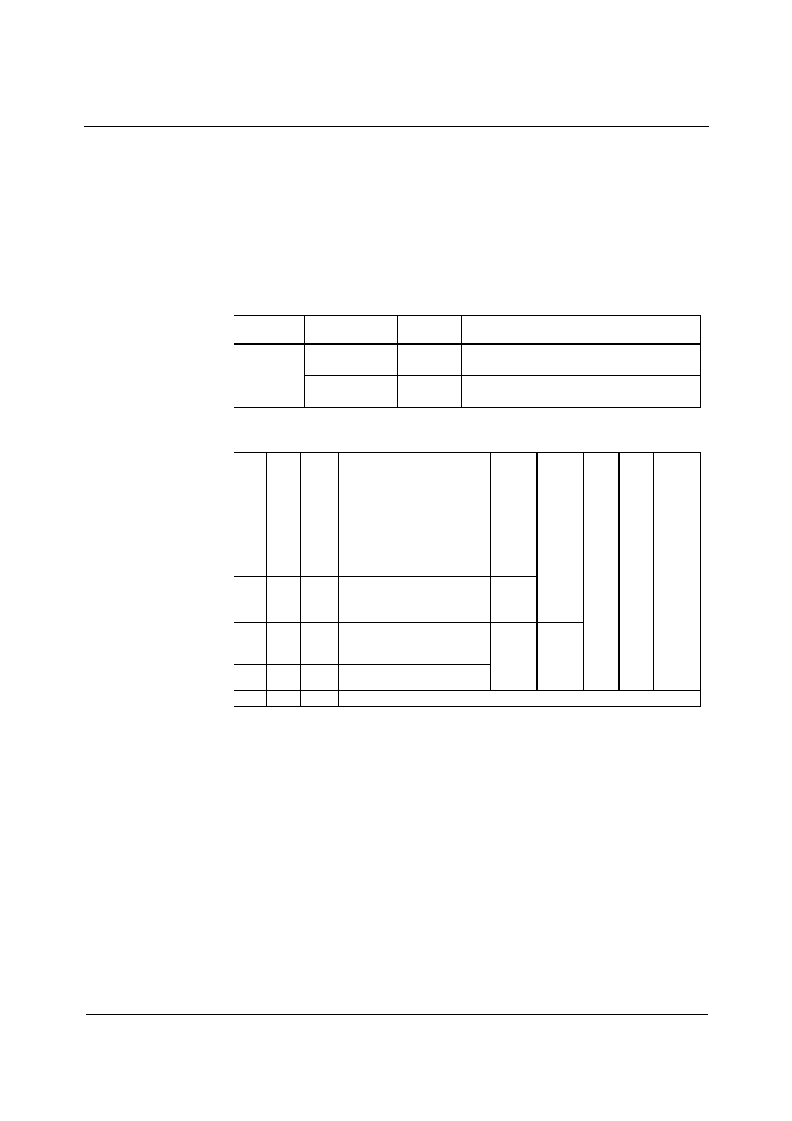
Production Data
WM9712L
w
PD Rev 4.0 December 2003
33
JACK INSERTION AND AUTO-SWITCHING
In a phone application, a BTL ear speaker may be connected across OUT3 and HPOUTL, and a
stereo headphone on HPOUTL and HPOUTR. Typically, only one of these two output devices is
used at any given time: when no headphone is plugged in, the BTL ear speaker is active, otherwise
the headphone is used.
The presence of a headphone can be detected using GPIO1 (pin 44) and an external pull-up resistor
(see "Applications Information" section for a circuit diagram). When the jack is inserted GPIO1 is
pulled low by a switch on the socket. When the jack is removed GPIO1 is pulled high by a resistor. If
the JIEN bit is set, the WM9712L automatically switches between headphone and ear speaker, as
shown below.
REGISTER
ADDRESS
BIT
LABEL
DEFAULT
DESCRIPTION
12
JIEN
0
Jack Insert Enable ≠ Takes output of GPIO1
logic
58h
Additional
Functional
Control
11
FRC
0
Force Ear Speaker Mode
See table below
Table 20 Jack Insertion / Auto-Switching (1)
JIEN FRC GPIO1
MODE DESCRIPTION
OU
T
3
ST
A
T
E
HPO
U
TL
VOL
U
ME
HPO
U
TR
VOL
U
ME
OU
T
3
VOL
U
ME
HPOU
TL/
HPO
U
TR
ST
A
T
E
0
0
X
Jack insert detection disabled
(headphone and ear speaker
can be used at the same
time)
Set by
reg.
24h
and
26h
1
0
0
Jack insert detection
enabled, headphone plugged
in
Dis
abl
ed
S
e
t
by
r
eg.
04h
1
X
1
Jack insert detection
enabled, headphone not
plugged in
0
1
X
Force Ear Speaker Mode
Set by
reg.
24h
and
26h
Set by
reg.
16h
S
e
t
by
r
eg.
04h
S
e
t
by
r
eg.
16h
S
e
t
by
r
eg.
24h
and 26h
1
1
X
Invalid; do not use this setting
Table 21 Jack Insertion / Auto-Switching (2)
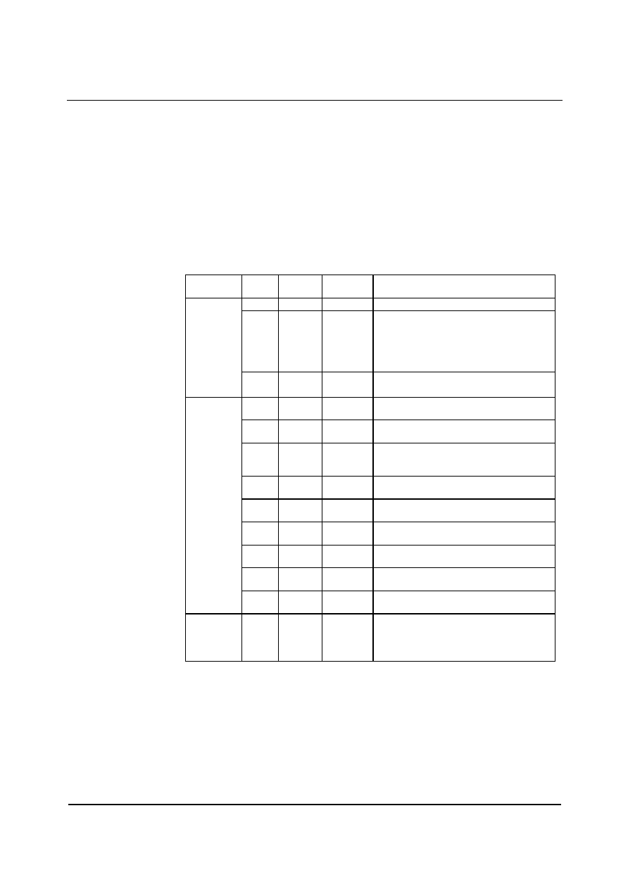
WM9712L
Production Data
w
PD Rev 4.0 December 2003
34
DIGITAL AUDIO (SPDIF) OUTPUT
The WM9712L supports the SPDIF standard using pin 47 as its output. Note that pin 47 can also be
used as a GPIO pin. The GE5 bit (register 56h, bit 5) selects between GPIO and SPDIF functionality
(see "GPIO and Interrupt control" section).
Register 3Ah is a read/write register that controls SPDIF functionality and manages bit fields
propagated as channel status (or sub-frame in the V case). With the exception of V, this register
should only be written to when the SPDIF transmitter is disabled (SPDIF bit in register 2Ah is `0').
Once the desired values have been written to this register, the contents should be read back to
ensure that the sample rate in particular is supported, then SPDIF validity bit SPCV in register 2Ah
should be read to ensure the desired configuration is valid. Only then should the SPDIF enable bit in
register 2Ah be set. This ensures that control and status information start up correctly at the
beginning of SPDIF transmission.
REGISTER
ADDRESS
BIT
LABEL
DEFAULT
DESCRIPTION
10
SPCV
0
SPDIF validity bit (read-only)
5:4
SPSA
01
SPDIF slot assignment (ADCO = 0)
00: Slots 3, 4
01: Slots 6, 9
10: Slots 7, 8
11: Slots 10, 11
2Ah
Extended
Audio
2
SEN
0
SPDIF output enable
1 = enabled, 0 = disabled
15
V
0
Validity bit; `0' indicates frame valid, `1'
indicates frame not valid
14
DRS
0
Indicates that the WM9712L does not support
double rate SPDIF output (read-only)
13:12
SPSR
10
Indicates that the WM9712L only supports
48kHz sampling on the SPDIF output (read-
only)
11
L
0
Generation level; programmed as required by
user
10:4
CC
0000000
Category code; programmed as required by
user
3
PRE
0
Pre-emphasis; `0' indicates no pre-emphasis,
`1' indicates 50/15us pre-emphasis
2
COPY
0
Copyright; `0' indicates copyright is not
asserted, `1' indicates copyright
1
AUDIB
0
Non-audio; `0' indicates data is PCM, `1'
indicates non-PCM format (e.g. DD or DTS)
3Ah
SPDIF
Control
Register
0
PRO
0
Professional; `0' indicates consumer, `1'
indicates professional
5Ch
Additional
Function
Control
4
ADCO
0
Source of SPDIF data
0: SPDIF data comes from SDATAOUT (pin
5), slot selected by SPSA
1: SPDIF data comes from audio ADC
Table 22 SPDIF Output Control
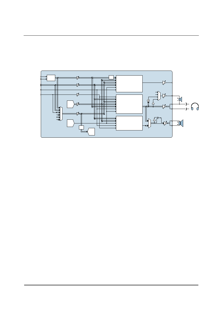
Production Data
WM9712L
w
PD Rev 4.0 December 2003
35
AUDIO MIXERS
MIXER OVERVIEW
The WM9712L has three separate low-power audio mixers to cover all audio functions required by
smartphones, PDAs and handheld computers. The diagram below shows the routing of the analogue
audio signals into the mixers. The numbers at the mixer inputs refer to the control register bits that
control the volume and muting for that particular signal.
PHONE_IN
PCBEEP
LINE_IN
Stereo
headphone /
headset
HPOUTL
HPOUTR
HPVOL
(Reg 04h)
MONOOUT
(PHONE TX)
OUT3VOL
(Reg 16h)
LOUT2
ROUT2
OUT2VOL
(Reg 02h)
loud
speaker
OUT3
ear
speaker
0Ch [4:0]
10h [12:8,4:0]
18h [12:8,4:0]
RECORD
SELECT
0Eh [12:8,4:0]
MICR
MICL
DIFF /
STEREO/
MONO
(Reg 20h)
STEREO
DAC
AUX
DAC
(12-BIT)
1Ch / ALC
0/20
dB
0Eh [7]
M
U
X
MONOOUT
VREF
18h [15]
10h [15]
14h [15:12]
14h [11:7]
0Ch [15]
12h [15:12]
18h [13]
10h [13]
0Eh [14,13]
1Ah [13:11]
0Ah [15:12]
HEAD
PHONE/
EAR
SPEAKER
MIX
PHONE
MIX
12h [7:4]
0Ah [7:4]
-1
M
U
X
12h [11:8]
18h [14]
10h [14]
0Ah [11:8]
0Ch [14]
BACK
SPEAKER
MIX
SRC
(Reg 16h)
OUT3SRC
(Reg 16h)
STEREO
ADC
M
U
X
PHONE MIX
HEADPHONE MIX
BACK SPKR MIX
INV
(Reg 02h)
1Ah [14]
0/20
dB
Figure 4 Audio Mixer Overview
HEADPHONE MIXER
The headphone mixer drives the HPOUTL and HPOUTR outputs. It also drives OUT3, if this pin is
connected to an ear speaker (phone receiver). The following signals can be mixed into the
headphone path:
∑
PHONE (controlled by register 0Ch, see "Audio Inputs")
∑
LINE_IN (controlled by register 10h, see "Audio Inputs")
∑
the output of the Record PGA (see "Audio ADC", "Record Gain")
∑
the stereo DAC signal (controlled by register 18h, see "Audio DACs")
∑
the MIC signal (controlled by register 0Eh, see "Audio Inputs")
∑
PC_BEEP (controlled by register 0Ah, see "Audio Inputs")
∑
the AUXDAC signal (controlled by register 12h, see "Auxiliary DAC")
In a typical smartphone application, the headphone signal is a mix of PHONE and sidetone (for
phone calls) and the stereo DAC signal (for music playback).

WM9712L
Production Data
w
PD Rev 4.0 December 2003
36
SPEAKER MIXER
The speaker mixer drives the LOUT2 and ROUT2 output. The following signals can be mixed into the
speaker path:
∑
PHONE (controlled by register 0Ch, see "Audio Inputs")
∑
LINE_IN (controlled by register 10h, see "Audio Inputs")
∑
the stereo DAC signal (controlled by register 18h, see "Audio DACs")
∑
PC_BEEP (controlled by register 0Ah, see "Audio Inputs")
∑
the AUXDAC signal (controlled by register 12h, see "Auxiliary DAC")
In a typical smartphone application, the speaker signal is a mix of AUXDAC (for system alerts or ring
tone playback), PHONE (for speakerphone function), and PC_BEEP (for externally generated ring
tones).
MONO MIXER
The mono mixer drives the MONOOUT pin. The following signals can be mixed into MONOOUT:
∑
LINE_IN (controlled by register 10h, see "Audio Inputs")
∑
the output of the Record PGA (see "Audio ADC", "Record Gain")
∑
the stereo DAC signal (controlled by register 18h, see "Audio DACs")
∑
the MIC signal (controlled by register 10h, see "Audio Inputs")
∑
PC_BEEP (controlled by register 0Ah, see "Audio Inputs")
∑
the AUXDAC signal (controlled by register 12h, see "Auxiliary DAC")
In a typical smartphone application, the MONOOUT signal is a mix of the amplified microphone
signal (possibly with Automatic Gain Control) and (if enabled) an audio playback signal from the
stereo DAC or the auxiliary DAC.
SIDE TONE CONTROL
The side tone path is into the headphone mixer and is either from the MIC or ALC path (with no 20dB
boost)
REGISTER
ADDRESS
BIT
LABEL
DEFAULT
DESCRIPTION
15
STM
1
MIC side tone select
0: selected
1 : not selected (path muted)
14:12
STVOL
010
(0dB)
MIC Sidetone volume
000 : +6dB (max.)
001: +3dB
... (3dB steps)
111 : -15dB (min.)
11:10
ALCM
11
ALC side tone select
11: mute
10: mono ≠ left
01: mono ≠ right
00: stereo
14h
Sidetone
Control
9:7
ALCVOL
010
(0dB)
ALC Sidetone volume
Similar to STVOL
Table 23 Side Tone Control

Production Data
WM9712L
w
PD Rev 4.0 December 2003
37
VARIABLE RATE AUDIO / SAMPLE RATE CONVERSION
By using an AC'97 Rev2.2 compliant audio interface, the WM9712L can record and playback at all
commonly used audio sample rates, and offer full split-rate support (i.e. the DAC, ADC and
AUXDAC sample rates are completely independent of each other ≠ any combination is possible).
The default sample rate is 48kHz. If the VRA bit in register 2Ah is set and the appropriate block is
enabled, then other sample rates can be selected by writing to registers 2Ch, 32h and 2Eh. The AC-
Link continues to run at 48k frames per second irrespective of the sample rate selected. However, if
the sample rate is less than 48kHz, then some frames do not carry an audio sample.
REGISTER
ADDRESS
BIT
LABEL
DEFAULT
DESCRIPTION
2Ah
Extended
Audio
Stat/Ctrl
0
VRA
0 (OFF)
Variable Rate Audio
0: OFF (DAC and ADC run at 48kHz)
1: ON (sample rates determined by
registers 2Ch, 2Eh and 32h)
2Ch
Audio DAC
Sample Rate
15:0
DACSR
BB80h
(48kHz)
Audio DAC sample rate
1F40h: 8kHz
2B11h: 11.025kHz
2EE0h: 12kHz
3E80h: 16kHz
5622h: 22.05kHz
5DC0h: 24kHz
7D00h: 32kHz
AC44h: 44.1kHz
BB80h: 48kHz
Any other value defaults to the nearest
supported sample rate
32h
Audio ADC
Sample Rate
15:0
ADCSR
BB80h
(48kHz)
Audio ADC sample rate
similar to DACSR
2Eh
AUXDAC
Sample Rate
15:0
AUXDA
CSR
BB80h
(48kHz)
AUXDAC sample rate
similar to DACSR
Table 24 Audio Sample Rate Control
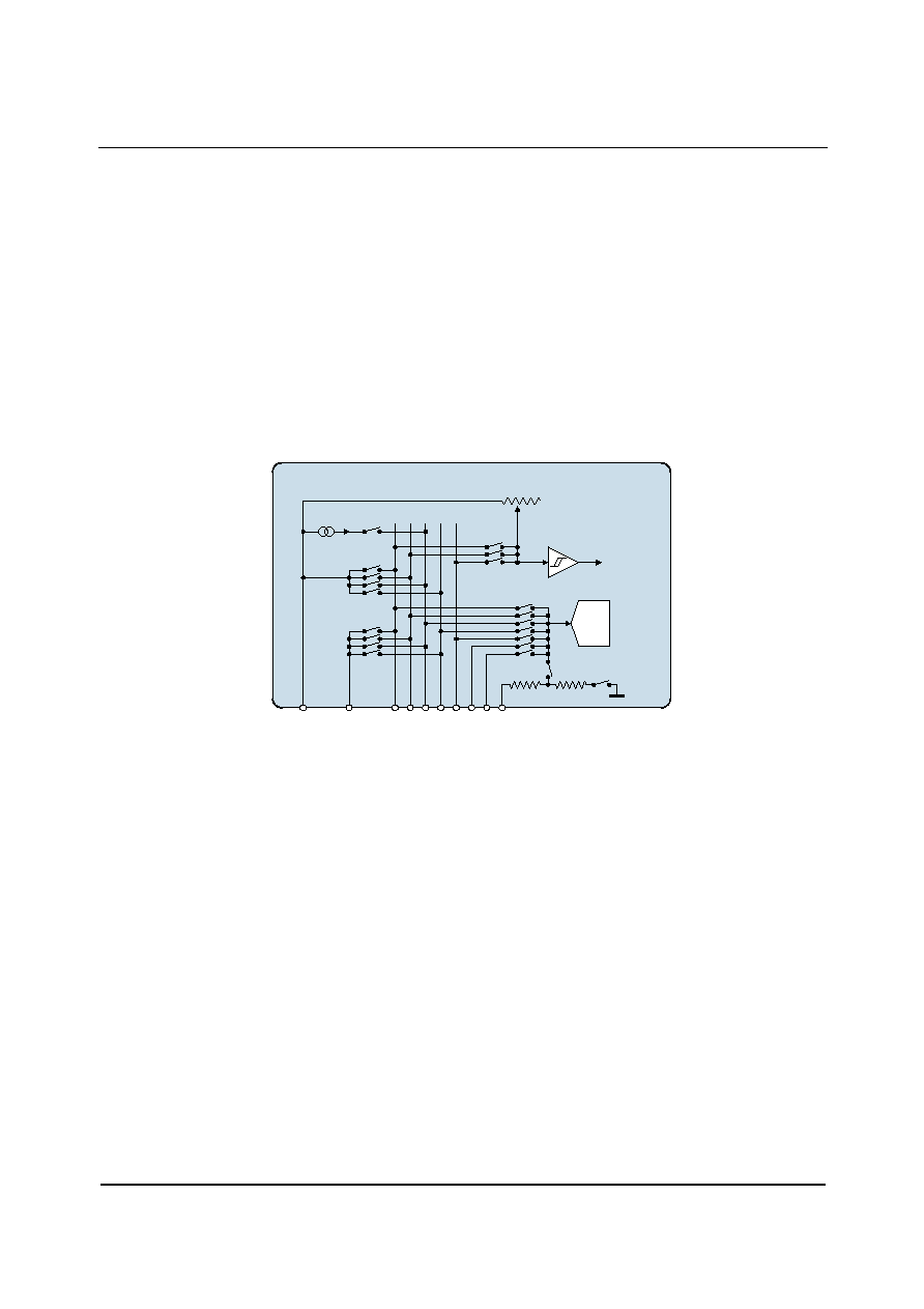
WM9712L
Production Data
w
PD Rev 4.0 December 2003
38
TOUCHPANEL INTERFACE
The WM9712L includes a touchpanel driver and digitiser circuit for use with 4-wire or 5-wire resistive
touchpanels. The following functions are implemented:
∑
X co-ordinate measurement
∑
Y co-ordinate measurement
∑
Pen down detection, with programmable sensitivity
∑
Touch pressure measurement (4-wire touchpanel only)
∑
Auxiliary measurement from COMP1/AUX1 (pin 29), COMP2/AUX2 (pin 30),
BMON/AUX3 (pin 31), or WIPER/AUX4 (pin 12)
The touchpanel digitiser uses a very low power, 12-bit successive approximation type ADC. The
same ADC can also be used for battery and auxiliary measurements (see the "Battery Alarm and
Battery Measurement" and "Auxiliary ADC Inputs" sections).
An on-chip switch matrix connects each touchpanel terminal to the supply voltage TPVDD, to ground
(TPGND), or to the ADC input, as required.
SAR
ADC
X
+
/B
R
(
14)
X
-
/T
L (16)
TP
G
N
D
Y
+
/TR
(15)
Y
-
/B
L (17)
W
I
PE
R/
A
U
X4
(
1
2
)
AU
X3
/
B
M
O
N
(
3
1
)
zero power
comparator
I
P
TPVD
D
R
PU
PEN
DOWN
AU
X2
(
3
0
)
AU
X1
(
2
9
)
20K
10K
Figure 5 Touchpanel Switch Matrix
PRINCIPLE OF OPERATION - FOUR-WIRE TOUCHPANEL
Four-wire touchpanels are connected to the WM9712L as follows:
∑
Right side contact = X+ (pin 14)
∑
Left side contact = X- (pin 16)
∑
Top side contact = Y+ (pin 15)
∑
Bottom side contact = Y- (pin 17)
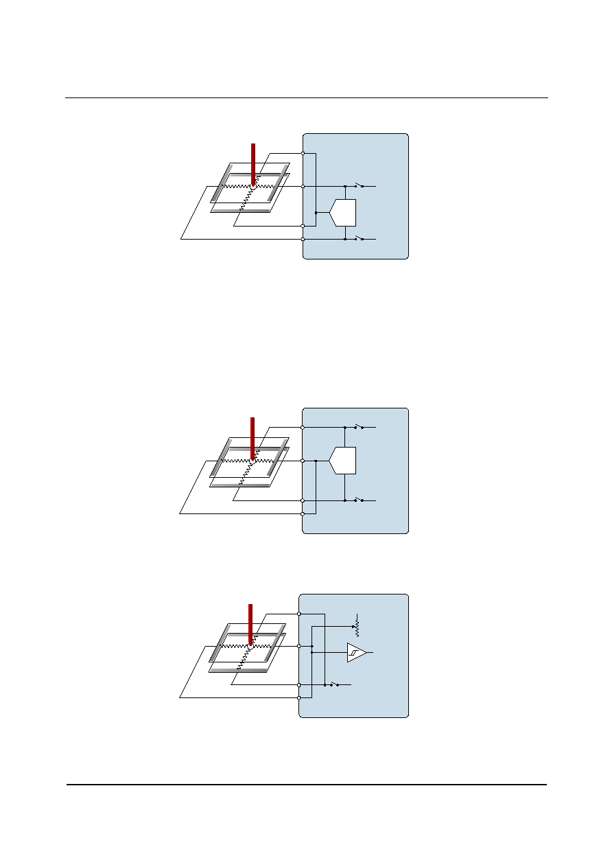
Production Data
WM9712L
w
PD Rev 4.0 December 2003
39
The principle of operation is illustrated below (Note: the illustrations assume that the top plate is used
for X and the bottom plate for Y measurements, although the reverse is also possible).
Y+ (15)
X+
(14)
Y- (17)
X- (16)
R
X+
R
Y-
pen / finger
R
Y+
R
X-
V
M
= (V
REF+
- V
REF-
) R
X-
/ (R
X-
+ R
X+
)
= proportional to X position
ADC
V
REF+
V
REF-
TPVDD
TPGND
WM9712
VM
Figure 6 X Co-ordinate Measurement on 4-wire Touchpanel
For an X co-ordinate measurement, the X+ pin is internally switched to VDD and X- to GND. The X
plate becomes a potential divider, and the voltage at the point of contact is proportional to its X co-
ordinate. This voltage is measured on the Y+ and Y- pins, which carry no current (hence there is no
voltage drop in R
Y+
or R
Y-
).
Due to the ratiometric measurement method, the supply voltage does not affect measurement
accuracy. The voltage references VREF+ and VREF- are taken from after the matrix switches, so
that any voltage drop in these switches has no effect on the ADC measurement.
Y+ (15)
X+
(14)
Y- (17)
X- (16)
R
X+
R
Y-
pen / finger
R
Y+
R
X-
V
M
= (V
REF+
- V
REF-
) R
Y-
/ (R
Y-
+ R
Y+
)
= proportional to Y position
ADC
V
REF+
V
REF-
TPVDD
TPGND
WM9712
VM
Figure 7 Y Co-ordinate Measurement on 4-wire Touchpanel
Y co-ordinate measurements are similar to X co-ordinate measurements, with the X and Y plates
interchanged.
zero power
comparator
Y+ (15)
X+
(14)
Y- (17)
X- (16)
R
X+
R
Y-
pen / finger
R
Y+
R
X-
TPGND
WM9712
PEN
DOWN
TPVDD
R
PU
Figure 8 Pen Down Detection on 4-wire Touchpanel
Pen down detection uses a zero power comparator (effectively a CMOS logic gate) with an internal,
programmable pull-up resistor R
PU
that controls pen-down sensitivity. Increasing R
PU
makes the
touchpanel less sensitive to touch, while lowering R
PU
makes it more sensitive.
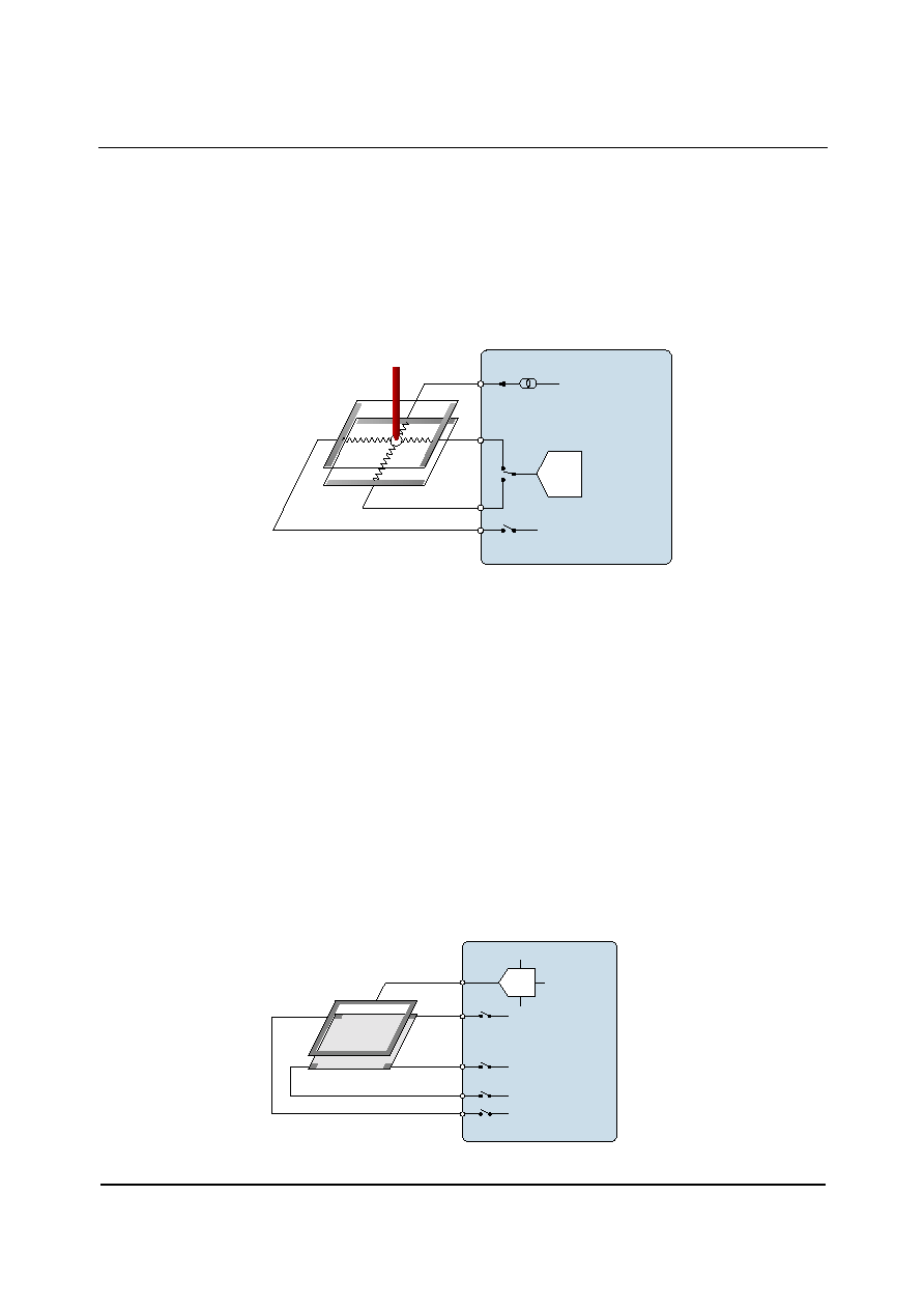
WM9712L
Production Data
w
PD Rev 4.0 December 2003
40
When the touchpanel is not being touched, no current flows in the circuit, and the PENDOWN signal
is low. When the panel is touched with a pen or finger, current flows through R
PU
and the panel, and
the comparator output goes high.
The PENDOWN signal can be read from bit 15 in register 7Ah (labeled PNDN). It can also be
observed on pin 46 (GPIO3 / PENDOWN), if the pin is not used for GPIO (GE3=0). Additionally,
PENDOWN is passed to the GPIO logic block (register 54h, bit 13), where it can generate CPU
interrupts, and / or to wake up the WM9712L from sleep mode (see "GPIO and Interrupt Control"
section).
I
P
Y+ (15)
X+
(14)
Y- (17)
X- (16)
R
X+
R
Y-
pen / finger
R
Y+
R
X-
TPGND
WM9712
TPVDD
ADC
V
Y-
- V
X+
= I
P
R
C
= proportional to contact resistance
Figure 9 Touch Pressure Measurement on 4-wire Touchpanel
Touch pressure can be determined indirectly by measuring the contact resistance R
C
between the
top and bottom plates. R
C
decreases as the touch pressure on the panel increases. The WM9712L
measures R
C
by sending a constant current I
P
through the touchpanel and measuring the potential
on each plate. The two values are subtracted in the digital domain to obtain the potential difference,
which is proportional to R
C
.
To suit different types of touchpanels, the magnitude of I
P
can be set to either 400
µ
A or 200
µ
A using
the PIL control bit.
PRINCIPLE OF OPERATION - FIVE-WIRE TOUCHPANEL
Five-wire touchpanels are connected to the WM9712Las follows:
∑
Top sheet contact = WIPER/AUX4 (pin 12)
∑
Top left corner of bottom sheet = TL (pin 16)
∑
Top right corner of bottom sheet = TR (pin 15)
∑
Bottom left corner of bottom sheet = BL (pin 17)
∑
Bottom right corner of bottom sheet = BR (pin 14)
V
M
= proportional to X position
WM9712
WIPER (12)
TR (15)
ADC
V
REF+
V
REF-
VM
TPGND
TPGND
TPVDD
TPVDD
BR (14)
BL (17)
TL (16)
Figure 10 X Co-ordinate Measurement on 5-wire Touchpanel
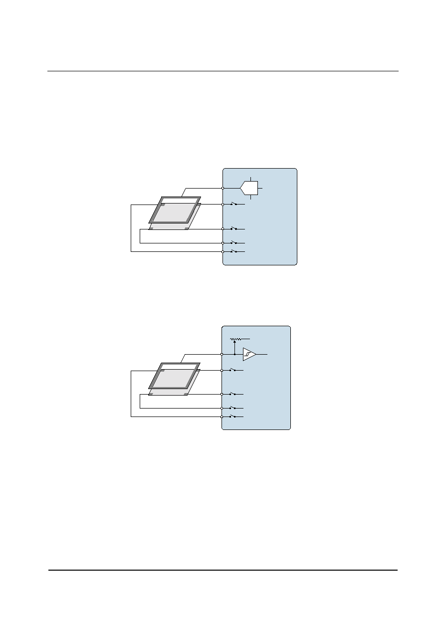
Production Data
WM9712L
w
PD Rev 4.0 December 2003
41
For an X co-ordinate measurement, the top left and bottom left corners of the touchpanel are
grounded internally to the WM9712, while the top right and bottom right contacts are connected to
TPVDD. The bottom plate becomes a potential divider with a voltage gradient in the X direction. The
voltage at the point of contact is proportional to its X co-ordinate. This voltage is measured on the
TOP pin and converted to a digital value by the ADC.
Due to the ratiometric measurement method, the supply voltage does not affect measurement
accuracy. The voltage references VREF+ and VREF- are taken from after the matrix switches, so
that any voltage drop in these switches has no effect on the ADC measurement.
V
M
= proportional to Y position
WM9712
WIPER (12)
TR (15)
ADC
V
REF+
V
REF-
VM
TPGND
TPVDD
TPGND
TPVDD
BR (14)
BL (17)
TL (16)
Figure 11 Y Co-ordinate Measurement on 5-wire Touchpanel
Y co-ordinate measurements are similar to Y co-ordinate measurements. However, the voltage
gradient on the bottom plate is in the Y direction instead of the X direction. This is achieved by
grounding the bottom left and bottom right corners of the touchpanel, and connecting the top left and
top right contacts to TPVDD.
WM9712
WIPER (12)
TR (15)
TPGND
TPGND
TPGND
TPGND
BR (14)
BL (17)
TL (16)
zero power
comparator
VDD
R
PU
PEN
DOWN
Figure 12 Pen Down Detection on 5-wire Touchpanel
Pen down detection works in a similar fashion for both 4-wire and 5-wire touchpanels (see Four-Wire
Touchpanel Operation). On a 5-wire touchpanel, all four contacts of the bottom plate are grounded,
and the top plate contact is connected to the internal programmable pull-up resistor, R
PU
.
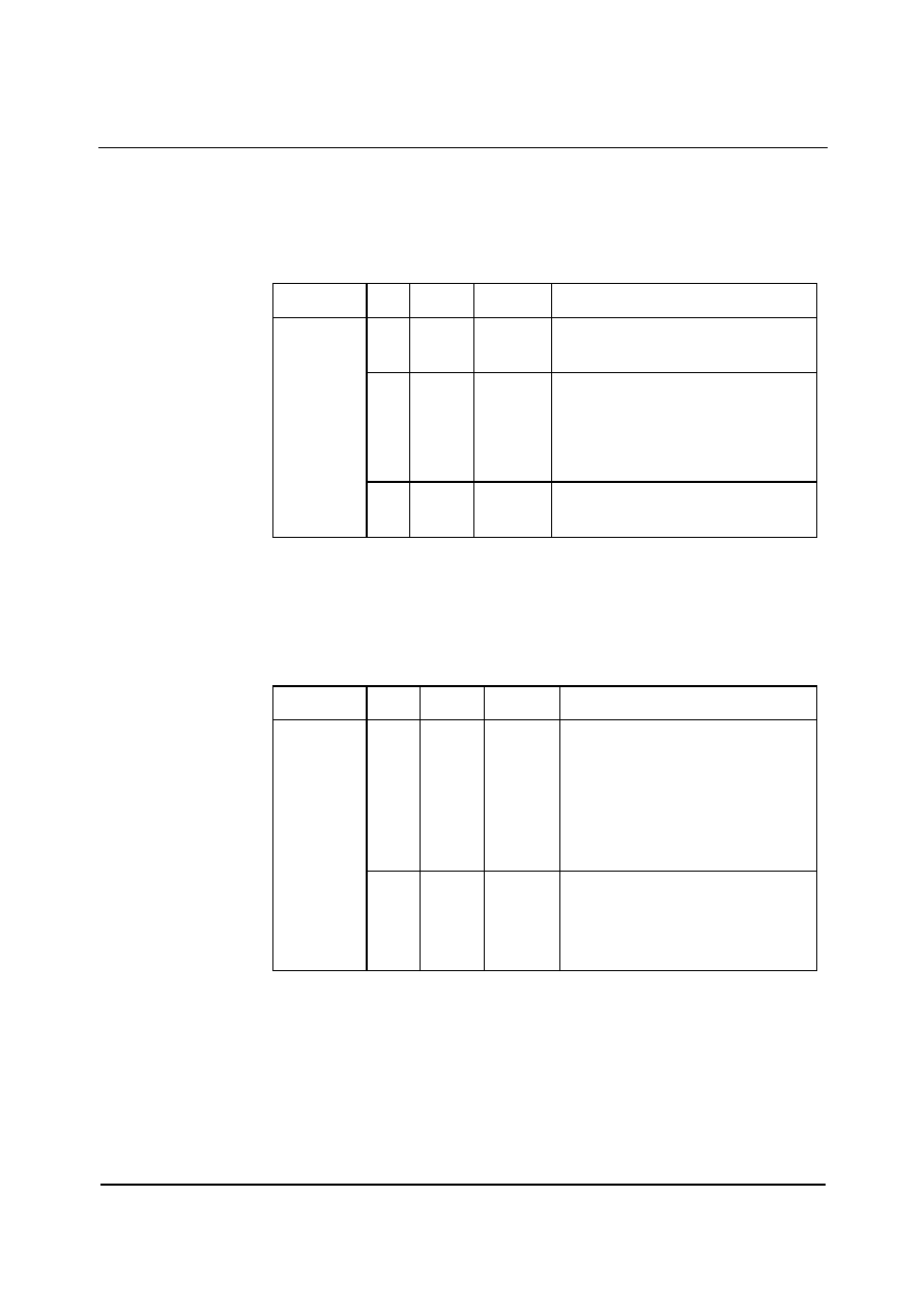
WM9712L
Production Data
w
PD Rev 4.0 December 2003
42
CONTROLLING THE TOUCHPANEL DIGITISER
All touchpanel functions are accessed and controlled through the AC-Link interface.
PHYSICAL CHARACTERISTICS
The physical characteristics of the touchpanel interface are controlled through register 78, as shown
below.
REGISTER
ADDRESS
BIT
LABEL
DEFAULT
DESCRIPTION
12
45W
0 (4-wire)
Touchpanel Type Selection
0: 4-wire
1: 5-wire
0:5
RPU
000001
(64k
)
Internal Pull-up resistor for Pen Detection
000000: RESERVED (do not use this setting)
000001: R
PU
/1 = TYP 64k
(most sensitive)
000010: R
PU
/2 = TYP 32k
... (pull-up = R
PU
/ binary value of RPU)
(Refer to page 9 for R
PU
specification)
78h
8
PIL
0 (200
µ
A)
Current used for pressure measurement
0: I
P
= 200
µ
A
1: I
P
= 400
µ
A
Table 25 Touchpanel Digitiser Control (Physical Characteristics)
POWER MANAGEMENT
To save power, the touchpanel digitiser and the pen-down detector can be independently disabled
when they are not used. The power consumption of the pen-down detector is normally negligible,
except when the pen is down.
The state of the digitiser and pen down detector is controlled by the following bits.
REGISTER
ADDRESS
BIT
LABEL
DEFAULT
DESCRIPTION
15:14
PRP
00
Pen ADC/AUX ADC enable
00 ≠ Pen digitiser off, pen detect off, no
wake-up on pen down (default)
01 ≠ Pen digitiser powered off, pen detect
enabled, touchpanel digitiser wakes up
(changes to state 11) on pen-down
10 ≠ Pen digitiser off, pen detect enabled,
no wake-up on pen down
11 ≠ Pen digitiser and pen detect enabled
78h
13
RPR
0
Wake-up on pen-down mode
0: Wake-up the AC-Link only (hold
SDATAIN high until controller sends warm
reset or cold reset)
1: Wake-up the WM9712L without waiting
for a reset signal from the controller
Table 26 Touchpanel Digitiser Control (Power Management)

Production Data
WM9712L
w
PD Rev 4.0 December 2003
43
INITIATION OF MEASUREMENTS
The WM9712L touchpanel interface supports both polling routines and DMA (direct memory access)
to control the flow of data from the touchpanel ADC to the host CPU.
In a polling routine, the CPU starts each measurement individually by writing to the POLL bit (register
76h, bit 15). This bit automatically resets itself when the measurement is completed.
REGISTER
ADDRESS
BIT
LABEL
DEFAULT
DESCRIPTION
10
CTC
0
0: Polling mode
1: Continuous mode (for DMA)
15
POLL
0
Writing "1" initiates a measurement
76h
9:8
CR
00
Continuous mode rate (DEL 1111)
00: 93.75 Hz (every 512 AC-Link frames)
01: 187.5 Hz (every 256 AC-Link frames)
10: 375Hz (every 128 AC-Link frames)
11: 750Hz (every 64 AC-Link frames)
Continuous mode rate (DEL = 1111)
00: 8 kHz (every six AC-Link frames)
01: 12 kHz (every four AC-Link frames)
10: 24 kHz (every other AC-Link frame)
11: 48 kHz (every AC-Link frame)
78h
11
PDEN
0
0: measure regardless of pen status
1: measure only when pen is down (when
CTC=0 and POLL=1, measurement is
delayed until pen-down; when CTC=1,
measurements are stopped on pen-up)
Table 27 Touchpanel Digitiser Control (Initiation of Measurements)
In continuous mode (CTC = 1), the WM9712L autonomously initiates measurements at the rate set
by CR, and supplies the measured data to the CPU on one of the unused AC'97 time slots. DMA-
enabled CPUs can write the data directly into a FIFO without any intervention by the CPU core. This
reduces CPU loading and speeds up the execution of user programs in handheld systems.
Note that the measurement frequency in continuous mode is also affected by the DEL bits (see
"Touchpanel Settling Time"). The faster rates achieved when DEL = 1111 may be useful when the
ADC is used for auxiliary measurements.
MEASUREMENT TYPES
The ADCSEL control bits determine which type of measurement is performed (see below).
REGISTER
ADDRESS
BIT
LABEL
DEFAULT
DESCRIPTION
14:12
ADCSEL
000
Measurement Type (ADC Input Selector)
000: No measurement
001: X co-ordinate measurement
010: Y co-ordinate measurement
011: Pressure measurement
100: COMP1/AUX1 measurement (pin 29)
101: COMP2/AUX2 measurement (pin 30)
110: BMON/AUX3 measurement (pin 31)
111: WIPER/AUX4 measurement (pin 12)
76h
11
COO
0
Enable co-ordinate mode
0: Single measurement according to ADCSEL
1: X, then Y, then additional measurement
indicated by ADCSEL
Table 28 Touchpanel Digitiser Control (Measurement Types)
WM9712L
Production Data
w
PD Rev 4.0 December 2003
44
When COO is `0', the WM9712L performs one type of measurement once (in polling mode) or
continuously (in continuous mode).
The co-ordinate mode (COO = `1') makes it easier to obtain co-ordinate pairs rather than single co-
ordinates. In polling-coordinate mode (CTC = `0', COO = `1'), the WM9712L performs an X
measurement, followed by a Y measurement, followed by an additional measurement determined by
ADCSEL, then stops. In continuous-coordinate mode (CTC = `1', COO = `1'), the WM9712L
continuously repeats a sequence consisting of an X-co-ordinate measurement, followed by a Y co-
ordinate measurement, followed by an additional measurement determined by ADCSEL (if ADCSEL
= 000, the sequence is XYXYXY... only).
DATA READBACK
The output data word of the touchpanel interface consists of three parts:
∑
Pen Status (1 bit) ≠ this is also passed to the GPIO logic block, which can be
programmed to generate an interrupt and/or wake up the WM9712L on pen down (see
GPIO and Interrupt Control).
∑
Output data from the touchpanel ADC (12 bits)
∑
ADCSRC: 3 additional bits that indicate the source of the ADC data. With COO = `0',
ADCSRC echoes ADCSEL. However, in co-ordinate mode (COO = `1'), the WM9712L
schedules different types of measurements autonomously and sets the ADCSRC bits
accordingly (see "Measurement Types").
This data is stored in register 7Ah, and can be retrieved by reading the register in the usual manner
(see AC-Link Interface section). Additionally, the data can also be passed to the controller on one of
the AC-Link time slots not used for audio functions.
If the data is being read back using the polling method, there are several ways to determine when a
measurement has finished:
∑
Reading back the POLL bit. If it has been reset to `0', then the measurement has finished.
∑
By monitoring the ADA signal, see GPIO and interrupt section
∑
Reading back 7Ah until the new data appears
REGISTER
ADDRESS
BIT
LABEL
DEFAULT
DESCRIPTION
15
PNDN
0
Pen status (read-only)
0: Pen Up
1: Pen Down
14:12
ADCSRC
000
Touchpanel ADC Source
000: No measurement
001: X co-ordinate measurement
010: Y co-ordinate measurement
011: Pressure measurement
(4-wire touchpanels only)
100: COMP1/AUX1 measurement (pin 29)
101: COMP2/AUX2 measurement (pin 30)
110: BMON/AUX3 measurement (pin 31)
111: WIPER/AUX4 measurement (pin 12)
7Ah
or
AC-Link slot
selected by
SLT
11:0
ADCD
000h
Touchpanel ADC Data (read-only)
Bit 11 = MSB
Bit 0 = LSB
78h
9
WAIT
0
0: No effect (new ADC data overwrites
unread data in register 7Ah)
1: New data is held back, and
measurements delayed, until register 7Ah is
read)
Table 29 Touchpanel Digitiser Data
To avoid losing data that has not yet been read, the WM9712L can delay overwriting register 7Ah
with new data until the old data has been read. This function is enabled using the WAIT bit.

Production Data
WM9712L
w
PD Rev 4.0 December 2003
45
If the SLEN bit is set to `1', then the touchpanel data appears on the AC-Link slot selected by the
SLT control bits, as shown below. The Slot 0 `tag' bit corresponding to the selected time slot is
asserted whenever there is new data on that slot.
REGISTER
ADDRESS
BIT
LABEL
DEFAULT
DESCRIPTION
3
SLEN
0
Slot Readback Enable
0: Disabled (readback through register only)
1: Enable (readback slot selected by SLT)
76h
2:0
SLT
110
AC'97 Slot Selection for Touchpanel Data
000: Slot 5
001: Slot 6
...
101: Slot 10
110: Slot 11
111: RESERVED
Table 30 Returning Touchpanel Data Through an AC-Link Time Slot
TOUCHPANEL SETTLING TIME
For accurate touchpanel measurements, some settling time may be required between the switch
matrix applying a voltage across the touchpanel plate and the ADC sampling the signal. This time
delay function is built into the WM9712L and can be programmed as shown below.
REGISTER
ADDRESS
BIT
LABEL
DEFAULT
DESCRIPTION
76h
7:4
DEL
0000
(1 frame)
Touchpanel ADC Settling Time
Table 31 Touchpanel Settling Time Control (1)
DEL
DELAY
(AC-LINK FRAMES)
DELAY
(TIME)
0000
1
20.8
µ
s
0001
2
41.7
µ
s
0010
4
83.3
µ
s
0011
8
167
µ
s
0100
16
333
µ
s
0101
32
667
µ
s
0110
48
1ms
0111
64
1.33ms
1000
96
2ms
1001
128
2.67ms
1010
160
3.33ms
1011
192
4ms
1100
224
4.67ms
1101
256
5.33ms
1110
288
6ms
1111
No delay, switch matrix always on
Table 32 Touchpanel Settling Time Control (2)
The total time for co-ordinate or auxiliary measurements to complete is the delay time DEL, plus one
AC-Link frame (20.8
µ
s). For a pressure measurement, the time taken is DEL plus two AC-Link
frames (41.6
µ
s).
WM9712L
Production Data
w
PD Rev 4.0 December 2003
46
Setting DEL to `1111' reduces the settling time to zero, i.e. measurements begin immediately. This
mode is intended for fast sampling on AUX inputs. It is NOT intended for touchpanel digitisation.
There are several side-effects when DEL is set to `1111':
∑
Co-ordinate mode does not work, i.e. the WM9712L behaves as if COO = 0, even if COO
= 1 (see "Measurement Types")
∑
If X / Y co-ordinate or touch pressure measurements are selected (ADCSEL = 001, 010
or 011), then the switch matrix is constantly on, and current constantly flows in the
touchpanel. This increases power consumption in the system, and is therefore not
recommended for battery powered systems
∑
In continuous mode (CTC = 1), setting DEL = 1111 increases the sampling rate of the
touchpanel ADC (see "Initiation of Measurements")
MASK INPUT CONTROL
Sources of glitch noise, such as the signals driving an LCD display, may feed through to the
touchscreen plates and affect measurement accuracy. In order to minimise this effect, a signal may
be applied to MASK (pin 47) to delay or synchronise the sampling of any input to the ADC. The effect
of the MASK signal depends on the the MSK[1-0] bits of register 78h, as described below.
MSK[1-0]
EFFECT OF SIGNAL ON MASK PIN
00
Mask has no effect on conversions GPIO input disabled (default)
01
Static; `hi' on MASK pin stops conversions, `lo' has no effect.
10
Edge triggered; rising or falling edge on MASK pin delays conversions
by an amount set in the DEL[3-0] register. Conversions are asynchronous to
the MASK signal.
11
Synchronous mode; conversions wait until rising or falling edge on MASK
initiates cycle; screen starts to be driven when the edge arrives, the
conversion sample being taken a period set by DEL[3-0] after the edge.
Table 33 Controlling the MASK Feature
Note that pin 47 can also be used as a GPIO(see "GPIO and Interrupt Control" section), or to output
the ADA signal (see below).
THE ADA SIGNAL
Whenever data becomes available from the touchpanel ADC, the internal ADA (ADC Data Available)
signal goes high and remains high until the data has been read from register 7Ah (if SLEN = 0) or
until it has been sent out on an AC-Link slot (if SLEN = 1).
ADA can be used to generate an interrupt, if the AW bit (register 52h, bit 12) is set (see "GPIO and
interrupt control" section)
It is also possible to output the ADA signal on pin 47, if this pin is not used as a GPIO. The GE4 bit
(register 56h, bit 12) must be set to `0' to achieve this (see "GPIO and interrupt control" section).
Alternatively, ADA can be read from bit 12 in register 54h.

Production Data
WM9712L
w
PD Rev 4.0 December 2003
47
AUXILIARY ADC INPUTS
The ADC used for touchpanel digitisation can also be used for auxiliary measurements, provided that
it is enabled (register 78h, PRP = 11). The WM9712L has four pins that can be used as auxiliary
ADC inputs:
∑
COMP1 / AUX1 (pin 29)
∑
COMP2 / AUX2 (pin 30)
∑
BMON / AUX3 (pin 31)
∑
WIPER / AUX4 (pin 12)
Note that pin 12 connects to the wiper of a 5-wire touchpanel wiper function. Auxiliary measurements
taken on pin 12 are only meaningful when it is not connected to a touchpanel (i.e. a 4-wire
touchpanel, or no touchpanel at all, is used). Pins 29 and 30 are also used as comparator inputs (see
Battery Alarm and Battery Measurement), but auxiliary measurements can still be taken on these
pins at any time. For the use of pin 31 see the "Battery Alarm And Battery Measurement" section,
note that the measured value from the BMON/AUX3 pin will be 1/3 of the actual value due to the
potential divider on this pin. The ADCSEL control bits select between different ADC inputs, as shown
below.
REGISTER
ADDRESS
BIT
LABEL
DEFAULT
DESCRIPTION
76h
Touchpanel
Digitiser
Control
14:12
ADCSEL
000
Touchpanel ADC Input Selector
000: No measurement
001-011: Touchpanel measurement (please
refer to Touchpanel Digitiser section)
100: COMP1 / AUX1 measurement (pin 29)
101: COMP2 AUX2 measurement (pin 30)
110: BMON / AUX3 measurement (pin 31)
111: WIPER / AUX 4 measurement (pin 12)
Table 34 Auxiliary ADC Measurements
Auxiliary ADC measurements are initiated in the same way as touchpanel measurements, and the
data is returned in the same manner. Please refer to the "Controlling the Touchpanel Interface"
section.
BATTERY MEASUREMENT USING THE BMON/AUX3 PIN
BMON/AUX3 (pin 31) has the capability to take inputs up to 5 volts (Assuming AVDD=3.3V) by
dividing down the input signal. The internal potential divider has a total resistance of 30k
. However,
it is only connected to the pin when an AUX3 measurement is requested, and remains connected for
the duration of one AC-Link frame (20.83
µ
s, assuming a 24.576MHz clock crystal is used). The
effective input impedance of BMON/AUX3 is therefore given by:
R
BMON
= 30k
◊
48kHz / [BMON sampling rate]
For example, if BMON is sampled ten times per second, the effective input resistance is 30k
◊
48kHz / 10Hz = 144M
.
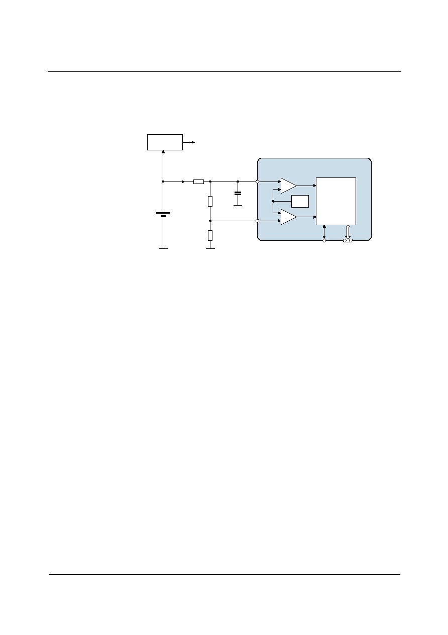
WM9712L
Production Data
w
PD Rev 4.0 December 2003
48
BATTERY ALARM AND ANALOGUE COMPARATORS
The battery alarm function differs from battery measurement in that it does not actually measure the
battery voltage. Battery alarm only indicates "OK", "Low" or "Dead". The advantage of the battery
alarm function is that it does not require a clock and can therefore be used in low-power sleep or
standby modes.
AUX1/
COMP1
AUX2/
COMP2
+
-
-
+
V
REF
GPIO2/
IRQ
GPIO
PINS
DEAD
BAT
LOW
BAT
GPIO /
INTERRUPT
LOGIC
C
R2
R3
R1
V
BATT
WM9712L
I
ALARM
VOLTAGE
REGULATOR
AVDD, DCVDD, ...
Figure 13 Battery Alarm Example Schematic
The typical schematic for a dual threshold battery alarm is shown above. This alarm has two
thresholds, "dead battery" (COMP1) and "low battery" (COMP2). R1, R2 and R3 set the threshold
voltages. Their values can be up to about 1M
in order to keep the battery current [I
ALARM
= V
BATT
/
(R1+R2+R3)] to a minimum (higher resistor values may affect the accuracy of the system as leakage
currents into the input pins become significant).
∑
Dead battery alarm: COMP1 triggers when V
BATT
< VREF
◊
(R1+R2+R3) / (R2+R3)
A dead battery alarm is the highest priority of interrupt in the system. It should immediately save all
unsaved data and shut down the system. The GP15, GS15 and GW15 bits must be set to generate
this interrupt.
∑
Low battery alarm: COMP2 triggers when V
BATT
< VREF
◊
(R1+R2+R3) / R3
A low battery alarm has a lower priority than a dead battery alarm. Since the threshold voltage is
higher than for a dead battery alarm, there is enough power left in the battery to give the user a
warning and/or shut down "gracefully". When V
BATT
gets close to the low battery threshold, spurious
alarms are filtered out by the COMP2 delay function.
The purpose of the capacitor C is to remove from the comparator inputs any high frequency noise or
glitches that may be present on the battery (for example, noise generated by a charge pump). It
forms a low pass filter with R1, R2 and R3.
∑
Low pass cutoff f
c
[Hz] = 1/ (2
C
◊
(R1 || (R2+R3)))
Provided that the cutoff frequency is several orders of magnitude lower than the noise frequency f
n
,
this simple circuit can achieve excellent noise rejection.
∑
Noise rejection [dB] = 20 log (f
n
/ f
c
)
The circuit shown above also allows for measuring the battery voltage V
BATT
. This is achieved simply
by setting the touchpanel ADC input to be either COMP1 (ADCSEL = 100) or COMP2 (ADCSEL =
101) (see also Auxiliary ADC Inputs).
Production Data
WM9712L
w
PD Rev 4.0 December 2003
49
The WM9712L has two on-chip comparators that can be used to implement a battery alarm function,
or other functions such as a window comparator. Each comparator has one of its inputs tied to any
one of three device pins and the other tied to a voltage reference. The voltage reference can be
either internally generated (VREF = AVDD/2) or externally connected on AUX4 (pin 12).
The comparator output signals are passed to the GPIO logic block (see "GPIO and Interrupt Control"
section), where they can be used to send an interrupt to the CPU via the AC-Link or via the IRQ pin,
and / or to wake up the WM9712L from sleep mode. COMP1/AUX1 (pin 29) corresponds to GPIO bit
15 and COMP2/AUX2 (pin30) to bit 14.
REGISTER
ADDRESS
BIT
LABEL
DEFAULT
DESCRIPTION
15
CP1
1
COMP1 Polarity (see also "GPIO and Interrupt
Control")
0: Alarm when COMP1 voltage is above VREF
1: Alarm when COMP1 voltage is below VREF
4Eh
14
CP2
1
COMP2 Polarity (see also "GPIO and Interrupt
Control")
0: Alarm when COMP2 voltage is above VREF
1: Alarm when COMP2 voltage is below VREF
58h
15:13
COMP2
DEL
0
Low Battery Alarm Delay
000: No delay
001: 0.17s (2
13
= 8192 AC-Link frames)
010: 0.34s (2
14
= 16384 AC-Link frames)
011: 0.68s (2
15
= 32768 AC-Link frames)
100: 1.4s (2
16
= 65536 AC-Link frames)
101: 2.7s (2
17
= 131072 AC-Link frames)
110: 5.5s (2
18
= 262144 AC-Link frames)
111: 10.9s (2
19
= 524288 AC-Link frames)
Table 35 Comparator Control
REGISTER
ADDRESS
BIT
LABEL
DEFAULT
DESCRIPTION
Comparator 1 Reference Voltage
0
VREF = AVDD/2
14
C1REF
0
1
WIPER/AUX4 (pin 12)
Comparator 1 Signal Source
00
AVDD/2 when C1REF='1'. Otherwise
comparator 1 is powered down
01
COMP1/AUX1 (pin 29)
10
COMP2/AUX2 (pin 30)
13:12
C1SRC
00
11
BMON/AUX3 (pin 31)
Comparator 2 Reference Voltage
0
VREF = AVDD/2
11
C2REF
0
1
WIPER/AUX4 (pin 12)
Comparator 2 Signal Source
00
AVDD/2 when C2REF='1'. Otherwise
comparator 2 is powered down
01
COMP1/AUX1 (pin 29)
10
COMP2/AUX2 (pin 30)
5Ch
Additional
Analogue
Functions
10:9
C2SRC
00
11
BMON/AUX3 (pin 31)
Table 36 Comparator Reference and Source Control

WM9712L
Production Data
w
PD Rev 4.0 December 2003
50
COMP2 DELAY FUNCTION
COMP2 has an optional delay function for use when the input signal is noisy. When COMP2 triggers
and the delay is enabled (i.e. COMP2DEL is non-zero), then GPIO bit 14 does not change state
immediately, and no interrupt is generated. Instead, the WM9712L starts a delay timer and checks
COMP2 again after the delay time has passed. If COMP2 is still active, then the GPIO bit is set and
an interrupt may be generated (depending on the state of the GW14 bit). If COMP2 is no longer
active, the GPIO bit is not set, i.e. all register bits are as if COMP2 had never triggered.
Note: If COMP2 triggers while the WM9712L is in sleep mode, and the delay is enabled, then the
device starts the on-chip crystal oscillator in order to count the time delay.
COMP2
TRIGGERS
START TIMER
COMP2?
WAIT
time=COMP2DEL
SHUT DOWN
TIMER
Inactive
Active
SET GI14
END
END
[FALSE ALARM]
COMP2
DEL?
non-zero
C2W?
0
END
1
000
Figure 14 COMP2 Delay Flow Chart
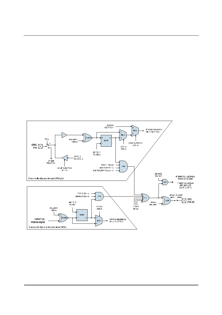
Production Data
WM9712L
w
PD Rev 4.0 December 2003
51
GPIO AND INTERRUPT CONTROL
The WM9712L has five GPIO pins that operate as defined in the AC'97 Revision 2.2 specification.
Each GPIO pin can be set up as an input or as an output, and has corresponding bits in register 54h
and in slot 12. The state of a GPIO output is determined by sending data through slot 12 of outgoing
frames (SDATAOUT). Data can be returned from a GPIO input by reading the register bit, or
examining slot 12 of incoming frames (SDATAIN). GPIO inputs can be made sticky, and can be
programmed to generate and interrupt, transmitted either through the AC-Link or through a
dedicated, level-mode interrupt pin (GPIO2/IRQ, pin 45).
GPIO pins 2 to 5 are multi-purpose pins that can also be used for other (non-GPIO) purposes, e.g.
as a SPDIF output or to signal pen-down. This is controlled by register 56h.
Independently of the GPIO pins, the WM9712L also has five virtual GPIOs. These are signals from
inside the WM9712L, which are treated as if they were GPIO input signals. From a software
perspective, virtual GPIOs are the same as GPIO pins, but they cannot be set up as outputs, and are
not tied to an actual pin. This allows for simple, uniform processing of different types of signals that
may generate interrupts (e.g. pen down, battery warnings, jack insertion, high-temperature warning,
or GPIO signals).
Figure 15 GPIO logic

WM9712L
Production Data
w
PD Rev 4.0 December 2003
52
GPIO
BIT
SLOT12
BIT
TYPE
PIN NO.
DESCRIPTION
1
5
GPIO Pin
44
GPIO1
2
6
GPIO Pin
45
GPIO2 / IRQ
enabled only when pin not used as IRQ
3
7
GPIO Pin
46
GPIO3 / PENDOWN
enabled only when pin not used as PENDOWN
4
8
GPIO Pin
47
GPIO4 / ADA / MASK
enabled only when pin not used as ADA
5
9
GPIO Pin
48
GPIO5 / SPDIF_OUT
enabled only when pin not used as
SPDIF_OUT
6-10
N/A
Unused
-
GPIO Logic not implemented for these bits
11
15
Virtual
GPIO
-
[Thermal Cutout]
Internal thermal cutout signal, indicates when
internal temperature reaches approximately
150
∞
C (see "Thermal Sensor")
12
16
virtual
GPIO
-
[ADA]
Internal ADA (ADC Data Available) Signal
enabled only when auxiliary ADC is active
13
17
Virtual
GPIO
-
[PEN DOWN]
Internal PENDOWN Signal
enabled only when pen-down detection is
active
14
18
Virtual
GPIO
-
[COMP2]
Internal COMP2 output (Low Battery Alarm)
enabled only when COMP2 is on
15
19
Virtual
GPIO
-
[COMP1]
Internal COMP1 output (Dead Battery Alarm)
enabled only when COMP1 is on
Table 37 GPIO Bits and Pins

Production Data
WM9712L
w
PD Rev 4.0 December 2003
53
The properties of the GPIOs are controlled through registers 4Ch to 52h, as shown below.
REGISTER
ADDRESS
BIT
LABEL
DEFAULT
DESCRIPTION
4Ch
n
GCn
1
GPIO Pin Configuration
0: Output
1: Input
GC11-15 are always `1'
Unused bits GC6-GC10 are always `0'
4Eh
n
GPn
1
GPIO Pin Polarity / Type
0: Active Low
1: Active High
[GIn = pin level XNOR GPn]
Unused bits GP6-GP10 are always `1'
50h
n
GSn
0
GPIO Pin Sticky
1: Sticky
0: Not Sticky
Unused bits GS6-GS10 are always `0'
52h
n
GWn
0
GPIO Pin Wake-up
1: Wake Up (generate interrupts from this pin)
0: No wake-up (no interrupts generated)
Unused bits GW6-GW10 are always `0'
54h
n
GIn
N/A
GPIO Pin Status
Read: Returns status of each GPIO pin
Write: Writing `0' clears sticky bit
Unused bits GI6-GI10 are always `0'
Table 38 GPIO Control
The following procedure is recommended for handling interrupts:
When the controller receives an interrupt, check register 54h. For each GPIO bit in descending order
of priority, check if the bit is `1'. If yes, execute corresponding interrupt routine, then write `0' to
corresponding bit in 54h. If no, continue to next lower priority GPIO. After all GPIOs have been
checked, check if the interrupt still present or no. If yes, repeat procedure. If no, then jump back to
process that ran before the interrupt.
If the system CPU cannot execute such an interrupt routine, it may be preferable to switch internal
signals (such as PENDOWN) directly onto the GPIO pins. However, in this case the interrupt signals
cannot be made sticky, and more GPIO pins are tied up both on the WM9712L and on the CPU.
WM9712L
Production Data
w
PD Rev 4.0 December 2003
54
REGISTER
ADDRESS
BIT
LABEL
DEFAULT
DESCRIPTION
2
GE2
1
GPIO2 / IRQ output select
0: Pin 45 disconnected from GPIO logic
set 4Ch, bit 2 to `0' to output IRQ signal
1: Pin 45 connected to GPIO logic (IRQ disabled)
3
GE3
1
GPIO3 / PENDOWN output select
0: Pin 46 disconnected from GPIO logic
set 4Ch, bit 3 to `0' to output PENDOWN signal
1: Pin 46 connected to GPIO logic
4
GE4
1
GPIO4 / ADA / MASK output select
0: Pin 47 disconnected from GPIO logic
set 4Ch, bit 4 to `0' to output ADA signal
set 4Ch, bit 4 to `1' to input MASK signal
1: Pin 47 connected to GPIO logic
56h
GPIO pins
function
select
5
GE5
1
GPIO5 / SPDIF output select
0: Pin 48 = SPDIF (disconnected from GPIO logic)
set 4Ch, bit 5 to `0' to output SPDIF signal
1: Pin 48 connected to GPIO logic (SPDIF
disabled)
Table 39 Using GPIO Pins for Non-GPIO Functions
REGISTER
ADDRESS
BIT
LABEL
DEFAULT
DESCRIPTION
0
IRQ INV
0
Inverts the IRQ signal (pin 45)
0: IRQ signal not inverted
1: IRQ signal inverted
58h
Additional
Functional
Control
1
WAKEEN
0
Enables GPIO wake-up
0: Disabled
1: Enabled
Table 40 Additional Functionality for GPIO Pins
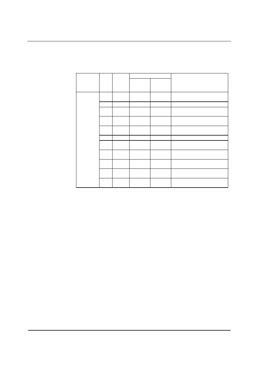
Production Data
WM9712L
w
PD Rev 4.0 December 2003
55
POWER MANAGEMENT
The WM9712L includes the standard power down control register defined by the AC'97 specification
(register 26h). Additionally, it also allows more specific control over the individual blocks of the device
through register 24h. Each particular circuit block is active when both the relevant bit in register 26h
AND the relevant bit in register 24h are set to `0'.
DEFAULT
REGISTER
ADDRESS
BIT
LABEL
NORMAL
PIN 47 `HI'
DURING
RESET
DESCRIPTION
14
PR6
0 (ON)
1 (OFF)
Disables HPOUTL, HPOUTR and
OUT3 Buffer
13
PR5
0 (ON)
1 (OFF)
Disables internal clock
12
PR4
0 (ON)
1 (OFF)
Disables AC-link interface
(external clock off)
11
PR3
0 (ON)
1 (OFF)
Disables VREF, analogue mixers
and outputs
10
PR2
0 (ON)
1 (OFF)
Disables analogue mixers,
LOUT2, ROUT2 (but not VREF)
9
PR1
0 (ON)
1 (OFF)
Disables stereo DAC
8
PR0
0 (ON)
1 (OFF)
Disables audio ADCs and input
Mux
3
REF
1
0
Read-only bit, indicates VREF is
ready (inverse of PR2)
2
ANL
1
0
Read-only bit, indicates analogue
mixers are ready (inverse of PR3)
1
DAC
1
0
Read-only bit, indicates audio
DACs are ready (inverse of PR1)
26h
Powerdown/
Status
register
0
ADC
1
0
Read-only bit, indicates audio
ADCs are ready (inverse of PR0)
Table 41 Powerdown and Status Register (Conforms to AC'97 Rev 2.2)
As can be seen from the table above, most blocks are `ON' by default. However, if pin 47
(GPIO4/ADA/MASK) is held high during reset, the WM9712L starts up with all blocks powered down
by default, saving power. This is achieved by connecting a pull-up resistor (e.g. 100k
) from pin 47
to DBVDD. Note that the state of pin 47 during reset only affects register 26h.
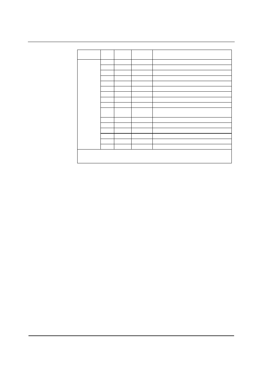
WM9712L
Production Data
w
PD Rev 4.0 December 2003
56
Table 42 Extended Power Down Register (Additional to AC'97 Rev 2.2)
Note:
*When disabling a PGA, always ensure that it is muted first.
ADDITIONAL POWER MANAGEMENT:
∑
AUXDAC: see "Auxiliary DAC" section. AUXDAC is OFF by default.
∑
Touchpanel Interface: see "Controlling the Touchpanel Digitiser / Power Management".
The touchpanel digitiser is OFF by default.
SLEEP MODE
Whenever the PR4 bit (reg. 26h) is set, the AC-Link interface is disabled, and the WM9712L is in
sleep mode. There is in fact a very large number of different sleep modes, depending on the other
control bits. For example, the low-power standby mode described below is a sleep mode. It is
desirable to use sleep modes whenever possible, as this will save power. The following functions do
not require a clock and can therefore operate in sleep mode:
∑
Analogue-to-analogue audio (DACs and ADCs unused), e.g. phone call mode
∑
Pen-down detection
∑
GPIO and interrupts
∑
Battery alarm / analogue comparators (but not battery measurement)
The WM9712L can awake from sleep mode as a result of
∑
A warm reset on the AC-Link (according to the AC'97 specification)
∑
A signal on a GPIO pin (if the pin is configured as an input, with wake-up enabled ≠ see
"GPIO and Interrupt Control" section)
∑
A virtual GPIO event such as pen-down, battery alarm, etc. (see "GPIO and Interrupt
Control" section)
REGISTER
ADDRESS
BIT
LABEL
DEFAULT
DESCRIPTION
15
PD15
0 (ON)
Disables Crystal Oscillator
14
PD14
0 (ON)
Disables left audio DAC
13
PD13
0 (ON)
Disables right audio DAC
12
PD12
0 (ON)
Disables left audio ADC
11
PD11
0 (ON)
Disables right audio ADC
10
PD10
0 (ON)
Disables MICBIAS
9
PD9
0 (ON)
Disables left headphone mixer
8
PD8
0 (ON)
Disables right headphone mixer
7
PD7
0 (ON)
Disables speaker mixer
6
PD6
0 (ON)
Disables MONO_OUT buffer (pin 33) and phone
mixer
5
PD5
0 (ON)
Disables OUT3 buffer (pin 37)
4
PD4
0 (ON)
Disables headphone buffers (HPOUTL/R)
3
PD3
0 (ON)
Disables speaker outputs (LOUT2, ROUT2)
2
PD2
0 (ON)
Disables Line Input PGA (left and right) *
1
PD1
0 (ON)
Disables Phone Input PGA *
24h
Additional
power down
control
0
PD0
0 (ON)
Disables Mic Input PGA (left and right) *
Note: When analogue inputs or outputs are disabled, they are internally connected to VREF
through a large resistor (VREF=AVDD/2 except in OFF mode, when VREF itself is disabled). This
maintains the potential at that node and helps to eliminate pops when the pins are re-enabled.
Production Data
WM9712L
w
PD Rev 4.0 December 2003
57
LOW POWER STANDBY MODE
If all the bits in registers 26h and 24h are set, then the WM9712L is in low-power standby mode and
consumes very little current. A 1M
resistor string remains connected across AVDD to generate
VREF. This is necessary if the on-chip analogue comparators are used (see "Battery Alarm and
Battery Measurement" section), and helps shorten the delay between wake-up and playback
readiness. If VREF is not required, the 1M
resistor string can be disabled by setting the SVD bit,
reducing current consumption further.
REGISTER
ADDRESS
BIT
LABEL
DEFAULT
DESCRIPTION
58h
10
SVD
0
VREF Disable
0: VREF enabled using 1M
string (low-power
standby mode)
1 : VREF disabled, 1M
string disconnected
(OFF mode)
Table 43 Disabling VREF (for lowest possible power consumption)
SAVING POWER AT LOW SUPPLY VOLTAGES
The analogue supplies to the WM9712L can run from 1.8V to 3.6V. By default, all analogue circuitry
on the IC is optimized to run at 3.3V. This set-up is also good for all other supply voltages down to
1.8V. However, at lower voltages, it is possible to save power by reducing the internal bias currents
used in the analogue circuitry. This is controlled as shown below.
REGISTER
ADDRESS
BIT
LABEL
DEFAULT
DESCRIPTION
5Ch
6:5
VBIAS
00
Analogue Bias optimization
11 : Lowest bias current, optimized for 1.8V
10 : Low bias current, optimized for 2.5V
01, 00 : Default bias current, optimized for 3.3V
Table 44 Analogue Bias Selection
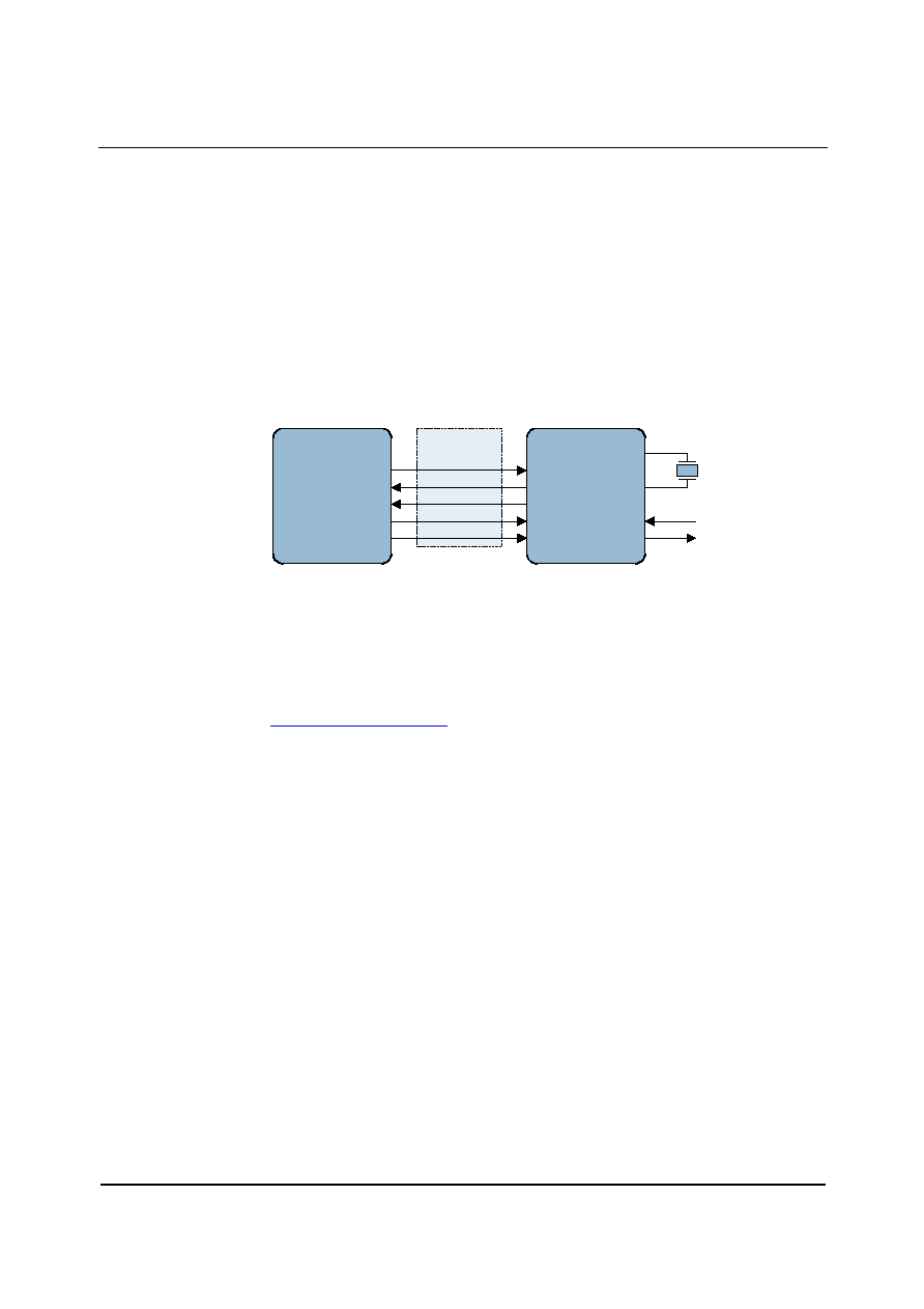
WM9712L
Production Data
w
PD Rev 4.0 December 2003
58
AC97 DATA AND CONTROL INTERFACE
INTERFACE PROTOCOL
The WM9712Lhas a single AC'97 interface for both data transfer and control. The AC-Link uses 5
wires:
∑
SDATAIN (pin 8) carries data from the WM9712L to the controller
∑
SDATAOUT (pin 5) carries data from the controller to the WM9712L
∑
BITCLK (pin 6) is a clock, normally generated by the WM9712L crystal oscillator and
supplied to the controller. However, BITCLK can also be passed to the WM9712L from
an off-chip generator.
∑
SYNC is a synchronization signal generated by the controller and passed to the
WM9712L
∑
RESETB resets the WM9712L to its default state
CONTROLLER
e.g. CPU
WM9712L
RESETB
SDATAIN
SDATAOUT
BITCLK
SYNC
24.576MHz
XTAL
AC-LINK
ANALOGUE
INPUTS /
OUTPUTS
Figure 16 AC-Link Interface (typical case with BITCLK generated by the AC97 codec)
The SDATAIN and SDATAOUT signals each carry 13 time-division multiplexed data streams (slots 0
to 12). A complete sequence of slots 0 to 12 is referred to as an AC-Link frame, and contains a total
of 256 bits. The frame rate is 48kHz. This makes it possible to simultaneously transmit and receive
multiple data streams (e.g. audio, touchpanel, AUXDAC, control) at sample rates up to 48kHz.
Detailed information can be found in the AC'97 (Revision 2.2) specification, which can be obtained at
www.intel.com/labs/media/audio/
Note:
SDATAOUT and SYNC must be held low for when RESETB is applied. These signals must be held
low for the entire duration of the RESETB pulse and especially during the low-to-high transition of
RESETB. If either is set high during reset the AC'97 device may enter test modes. Information
relating to this operation is available in the AC'97 specification or in Wolfson applications note WAN-
0104 available at www.wolfsonmirco.com.
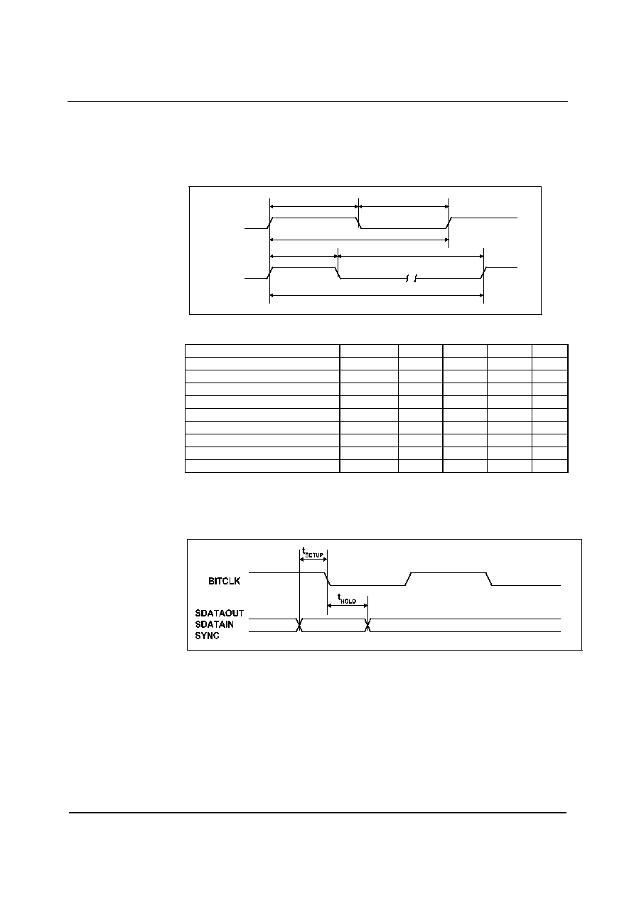
Production Data
WM9712L
w
PD Rev 4.0 December 2003
59
INTERFACE TIMING
Test Characteristics:
DBVDD = 3.3V, DCVDD = 3.3V, DGND1 = DGND2 = 0V, T
A
= -25
∞
C to +85
∞
C, unless otherwise stated.
CLOCK SPECIFICATIONS
BITCLK
SYNC
t
CLK_HIGH
t
CLK_LOW
t
CLK_PERIOD
t
SYNC_HIGH
t
SYNC_LOW
t
SYNC_PERIOD
Figure 17 Clock Specifications (50pF External Load)
PARAMETER
SYMBOL
MIN
TYP
MAX
UNIT
BITCLK frequency
12.288
MHz
BITCLK period
t
CLK_PERIOD
81.4
ns
BITCLK output jitter
750
ps
BITCLK high pulse width (Note 1)
t
CLK_HIGH
36
40.7
45
ns
BITCLK low pulse width (Note 1)
t
CLK_LOW
36
40.7
45
ns
SYNC frequency
48
kHz
SYNC period
t
SYNC_PERIOD
20.8
µ
s
SYNC high pulse width
t
SYNC_HIGH
1.3
µ
s
SYNC low pulse width
t
SYNC_LOW
19.5
µ
s
Note:
1. Worst case duty cycle restricted to 45/55
DATA SETUP AND HOLD
Figure 18 Data Setup and Hold (50pF External Load)
Note:
1.
Setup and hold times for SDATAIN are with respect to the AC'97 controller, not the
WM9712L.
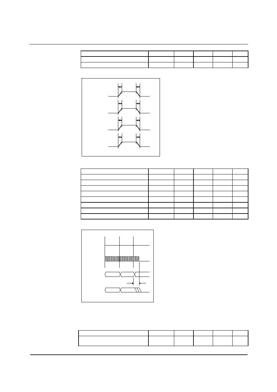
WM9712L
Production Data
w
PD Rev 4.0 December 2003
60
PARAMETER
SYMBOL
MIN
TYP
MAX
UNIT
Setup to falling edge of BITCLK
t
SETUP
10
ns
Hold from falling edge of BITCLK
t
HOLD
10
ns
SIGNAL RISE AND FALL TIMES
BITCLK
SYNC
SDATAIN
SDATAOUT
trise
CLK
tfall
CLK
trise
SYNC
tfall
SYNC
trise
DIN
tfall
DIN
trise
DOUT
tfall
DOUT
Figure 19 Signal Rise and Fall Times (50pF External Load)
PARAMETER
SYMBOL
MIN
TYP
MAX
UNIT
BITCLK rise time
trise
CLK
2
6
ns
BITCLK fall time
tfall
CLK
2
6
ns
SYNC rise time
trise
SYNC
2
6
ns
SYNC fall time
tfall
SYNC
2
6
ns
SDATAIN rise time
trise
DIN
2
6
ns
SDATAIN fall time
tfall
DIN
2
6
ns
SDATAOUT rise time
trise
DOUT
2
6
ns
SDATAOUT fall time
tfall
DOUT
2
6
ns
AC-LINK POWERDOWN
SYNC
BITCLK
SDATAOUT
WRITE
TO 0X20
DATA PR4
DON'T
CARE
SDATAIN
SLOT 1
SLOT 2
t
S2_PDOWN
Figure 20 AC-Link Powerdown Timing
AC-Link powerdown occurs when PR4 (register 26h, bit 12) is set (see "Power Management"
section).
PARAMETER
SYMBOL
MIN
TYP
MAX
UNIT
End of Slot 2 to BITCLK and SDATAIN
low
t
S2_PDOWN
1.0
µ
s
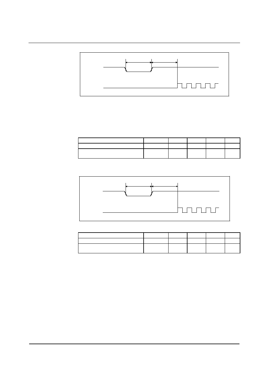
Production Data
WM9712L
w
PD Rev 4.0 December 2003
61
COLD RESET (ASYNCHRONOUS, RESETS REGISTER SETTINGS)
RESETB
BITCLK
t
RST_LOW
t
RST2CLK
Figure 21 Cold Reset Timing
Note:
For correct operation SDATAOUT and SYNC must be held LOW for entire RESETB active
low period otherwise the device may enter test mode. See AC'97 specification or Wolfson
applications note WAN104 for more details.
PARAMETER
SYMBOL
MIN
TYP
MAX
UNIT
RESETB active low pulse width
t
RST_LOW
1.0
µ
s
RESETB inactive to BITCLK startup
delay
t
RST2CLK
162.8
ns
WARM RESET (ASYNCHRONOUS, PRESERVES REGISTER SETTINGS)
SYNC
BIT_CLK
t
SYNC_HIGH
t
SYNC2CLK
Figure 22 Warm Reset Timing
PARAMETER
SYMBOL
MIN
TYP
MAX
UNIT
SYNC active high pulse width
t
SYNC_HIGH
1.3
µ
s
SYNC inactive to BITCLK startup
delay
t
RST2CLK
162.4
ns

WM9712L
Production Data
w
PD Rev 4.0 December 2003
62
REGISTER MAP
Note: Highlighted bits differ from the AC'97 specification (newly added for non-AC'97 function, or same bit used in a
different way, or for another function)
Reg
Name
15
14
13
12
11
10
9
8
7
6
5
4
3
2
1
0
Default
00hReset
0
SE4
SE3
SE2
SE1
SE0
ID9
ID8
ID7
ID6
ID5
ID4
ID3
ID2
ID1
ID0
6174h
02hLOUT2/ROUT2 Volume
MU
0
ZC
INV
8000h
04hHeadph
one Volume
MU
0
ZC
0
8000h
06hMONOOUT Volume
MU
0
0
0
0
0
0
0
ZC
0
0
8000h
08hDAC Tone Control
BB
0
0
BC
0
DAT
0
TC
0F0Fh
0AhPCBEEP Input
B2H
B2S
B2P
0
0
0
0
AAA0h
0ChPHONE Volume
P2H
P2S
0
0
0
0
0
0
0
0
0
C008h
0EhMIC Volume
0
M12P
M22P
20dB
6808h
10hLINEIN Volume
L2H
L2S
L2P
0
0
0
E808h
12hAUXDAC Volume / Routing
A2H
A2S
A2P
0
0
0
AXE
AAA0h
14hSidetone Volume
STM
0
0
0
0
0
0
0
AD00h
16hOUT3 Volume
MU
0
0
0
0
SRC
ZC
0
8000h
18hDAC Volume
D2H
D2S
D2P
0
0
0
E808h
1AhRecord Select
0
BOOST
R2P
BST
0
0
0
0
0
3000h
1ChRecord Gain
RMU
GRL
ZC
GRR
8000h
20hGeneral Purpose
0
0
3DE
0
0
0
0
0
LB
0
0
0
0
0
0
0
0000h
22hDAC 3D Control
0
0
0
0
0
0
0
0
0
0
3DLC
3DUC
0000h
24hPowerdown
PD15
PD14
PD13
PD12
PD11
PD10
PD9
PD8
PD7
PD6
PD5
PD4
PD3
PD2
PD1
PD0
0000h
26hPowerdown Ctrl/Stat
0
PR6
PR5
PR4
PR3
PR2
PR1
PR0
0
0
0
0
REF
ANL
DAC
ADC
000Fh
FF00h
28hExtended Audio ID
ID1
ID0
0
0
REV1
REV0
AMAP
LDAC
SDAC
CDAC
0
0
VRM
SPDIF
DRA
VRA
0405h
2AhExt'd Audio stst/ctrl
0
0
0
0
0
SPCV
0
0
0
0
0
SEN
0
VRA
0410h
2ChAudio DACs Sample Rate
BB80h
2EhAUXDAC Sample Rate
BB80h
32hAudio ADCs Sample Rate
BB80h
3AhSPDIF control
V
DRS
L
PRE
COPY AUD IB
PRO
2000h
4ChGPIO Pin Configuration
1
1
1
1
1
0
0
0
0
0
GC5
GC4
GC3
GC2
GC1
0
F83Eh
4EhGPIO Pin Polarity / Type
C1P
C2P
PP
AP
TP
1
1
1
1
1
GP5
GP4
GP3
GP2
GP1
1
FFFFh
50hGPIO Pin Sticky
C1S
C2S
PS
AS
TS
0
0
0
0
0
GS5
GS4
GS3
GS2
GS1
0
0000h
52hGPIO Pin Wake-Up
C1W
C2W
PW
AW
TW
0
0
0
0
0
GW5
GW4
GW3
GW2
GW1
0
0000h
54hGPIO Pin Status
C1I
C2I
PI
AI
TI
0
0
0
0
0
GI5
GI4
GI3
GI2
GI1
0
GPIO pins
56hGPIO Pin Sh
aring
1
1
1
1
1
0
0
0
0
0
GE5
GE4
GE3
GE2
1
0
F83Eh
58hAdditional Functions (1)
JIEN
FRC
SVD
0
0
0
0
0
0
WAKE
EN
IRQ
INV
0008h
5AhVendor Reserved
5ChAdd. Functions (2)
AMUTE
C1 REF
C2 REF
DS
AMEN
ADCO
HPF
ENT
0000h
5EhVendor Reserved
60hALC Control
B032h
62hALC / Noise Gate Control
ALC
ZC
NG AT
0
NGG
3E00h
64hAUXDAC input control
XSLE
0000h
66h-
74h
Vendor Reserved
76hDigitiser Reg 1
POLL
COO
CTC
SLEN
0006h
78hDigitiser Reg 2
RPR
45W
PDEN
0
WAIT
PIL
0001h
7AhDigitiser Read Back
PNDN
0000h
7ChVendor ID1
574Dh
7EhVendor ID2
4C12h
RESERVED FOR TEST
RESERVED. DO NOT WRITE TO THESE REGISTERS
OUT3 Volume
LOUT2 Volume
ROUT2 Volume
STVOL
LINEINLVOL
LINEINRVOL
A2HVOL
A2SVOL
B2HVOL
COMP2DEL
B2SVOL
SPSR
CC (Category Code)
ADCSR (Audio ADCs Sample Rate)
(Extended)
RECVOLL
RECVOLR
ASCII character "L"
"12" (indicates part number WM9712)
NGTH (threshold)
AUXDAC VAL
ASCII character "W"
ASCII character "M"
ALCSEL
CR
SLT
ADCD (TOUCHPANEL ADC DATA)
Die Revision
3DDEPTH
DACSR (Audio DACs Sample Rate)
AUXDACSR (Auxiliary DAC Sample Rate)
SPSA
Default for reg. 26h - pin 47 "low" or unconnected during reset
Default for reg. 26h - pin 47 "high" during reset (recommended for lowest power)
(Extended)
HPOUTR Volume
HPOUTL Volume
RECSL
RECSR
Left DAC Volume
Right DAC Volume
R2P
ALCM
ALCVOL
OUT3SRC
A2PVOL
MONOOUT Volume
BASS
TRBL
MICVOL (Mono /Right)
MS
B2PVOL
PHONEIN Volume
LMICVOL (Left Only)
C2SRC
AUXDACSLT
RPU
MSK
DEL
ASS
C1SRC
VBIAS
ALCL (target level)
HLD (hold time)
ADCSRC
PRP
RESERVED FOR TEST
MAXGAIN
ZC TIMEOUT
ADCSEL
DCY (decay time)
ATK (attack time)
Table 45 WM9712L Register Map
Production Data
WM9712L
w
PD Rev 4.0 December 2003
63
REGISTER BITS BY ADDRESS
Register 00h is a read-only register. Writing any value to this register resets all registers to their default, but does not
change the contents of reg. 00h. Reading the register reveals information about the codec to the driver, as required by the
AC'97 Specification, Revision 2.2
REG
ADDR
BIT
LABEL
DEFAULT
DESCRIPTION
REFER TO
14:10
SE [4:0]
11000
Indicates a codec from Wolfson Microelectronics
9:6
ID9:6
0101
Indicates 18 bits resolution for ADCs and DACs
5
ID5
1
Indicates that the WM9712L supports bass boost
4
ID4
1
Indicates that the WM9712L has a headphone output
3
ID3
0
Indicates that the WM9712L does not support simulated stereo
2
ID2
1
Indicates that the WM9712L supports bass and treble control
1
ID1
0
Indicates that the WM9712L does not support modem functions
00h
0
ID0
0
Indicates that the WM9712L does not have a dedicated microphone
ADC
Intel's AC'97
Component
Specification,
Revision 2.2,
page 50
Register 02h controls the output pins LOUT2 and ROUT2.
REG
ADDR
BIT
LABEL
DEFAULT
DESCRIPTION
REFER TO
15
MU
1 (mute)
Mutes LOUT2 and ROUT2.
13:8
LOUT2 VOL
000000 (0dB)
LOUT2 volume
7
ZC
0 (OFF)
Enables zero-cross detector
6
INV
0 (not inverted)
Inverts LOUT2 (for BTL speaker operation)
02h
5:0
ROUT2 VOL
000000 (0dB)
ROUT2 volume
Analogue
Audio Outputs
Register 04h controls the headphone output pins, HPOUTL and HPOUTR.
REG
ADDR
BIT
LABEL
DEFAULT
DESCRIPTION
REFER TO
15
MU
1 (mute)
Mutes HPOUTL and HPOUTR.
13:8
HPOUTL VOL
000000 (0dB)
HPOUTL volume
7
ZC
0 (OFF)
Enables zero-cross detector
04h
5:0
HPOUTR VOL
000000 (0dB)
HPOUTR volume
Analogue
Audio Outputs
Register 06h controls the analogue output pin MONOOUT.
REG
ADDR
BIT
LABEL
DEFAULT
DESCRIPTION
REFER TO
15
MU
1 (mute)
Mutes MONOOUT.
7
ZC
0 (OFF)
Enables zero-cross detector
06h
5:0
MONOOUT
VOL
000000 (0dB)
MONOOUT volume
Analogue
Audio Outputs
WM9712L
Production Data
w
PD Rev 4.0 December 2003
64
Register 08h controls the bass and treble response of the left and right audio DAC (but not AUXDAC).
REG
ADDR
BIT
LABEL
DEFAULT
DESCRIPTION
REFER TO
15
BB
0 (linear)
Selects linear bass control or adaptive bass boost
12
BC
0 (low)
Selects bass cut-off frequency
11:8
BASS
1111 (OFF)
Controls bass intensity
6
DAT
0 (OFF)
Enables 6dB pre-DAC attenuation
4
TC
0 (high)
Selects treble cut-off frequency
08h
3:0
TRBL
1111 (OFF)
Controls treble intensity
Audio DACs,
Tone Control /
Bass Boost
Register 0Ah controls the analogue input pin PCBEEP.
REG
ADDR
BIT
LABEL
DEFAULT
DESCRIPTION
REFER TO
15
B2H
1 (mute)
Mutes PCBEEP to headphone mixer path
14:12
B2HVOL
010 (0dB)
Controls gain of PCBEEP to headphone mixer path
11
B2S
1 (mute)
Mutes PCBEEP to speaker mixer path
10:8
B2SVOL
010 (0dB)
Controls gain of PCBEEP to speaker mixer path
7
B2P
1 (mute)
Mutes PCBEEP to phone mixer path
0Ah
6:4
B2PVOL
010 (0dB)
Controls gain of PCBEEP to phone mixer path
Analogue
Inputs,
PCBEEP Input
Register 0Ch controls the analogue input pin PHONE.
REG
ADDR
BIT
LABEL
DEFAULT
DESCRIPTION
REFER TO
15
P2H
1 (mute)
Mutes PHONE to headphone mixer path
14
P2S
1 (mute)
Mutes PHONE to speaker mixer path
0Ch
4:0
PHONEVOL
01000 (0dB)
Controls PHONE input gain to all mixers (but not to ADC)
Analogue
Inputs,
PHONE Input
Register 0Eh controls the analogue input pins MIC1 and MIC2.
REG
ADDR
BIT
LABEL
DEFAULT
DESCRIPTION
REFER TO
14
M12P
1 (mute)
Mutes MIC1 to phone mixer path
13
M22P
1 (mute)
Mutes MIC2 to phone mixer path
12:8
LMICVOL
01000 (0dB)
Controls volume of MIC1 (left), in stereo mode only
7
20dB
0 (OFF)
Enables 20dB gain boost
6:5
MS
00 (MIC1 only)
Selects microphone mode. 00=MIC1 only, 01=differential,
10=MIC2 only, 11=stereo
0Eh
4:0
MICVOL
01000 (0dB)
Controls mic volume (except MIC1 in stereo mode)
Analogue
Inputs,
Microphone
Input
Register 10h controls the analogue input pins LINEINL and LINEINR.
REG
ADDR
BIT
LABEL
DEFAULT
DESCRIPTION
REFER TO
15
L2H
1 (mute)
Mutes LINEIN to headphone mixer path
14
L2S
1 (mute)
Mutes LINEIN to speaker mixer path
13
L2P
1 (mute)
Mutes LINEIN to phone mixer path
12:8
LINEINLVOL
01000 (0dB)
Controls LINEINL input gain to all mixers (but not to ADC)
10h
4:0
LINEINRVOL
01000 (0dB)
Controls LINEINR input gain to all mixers (but not to ADC)
Analogue
Inputs, Line
Input
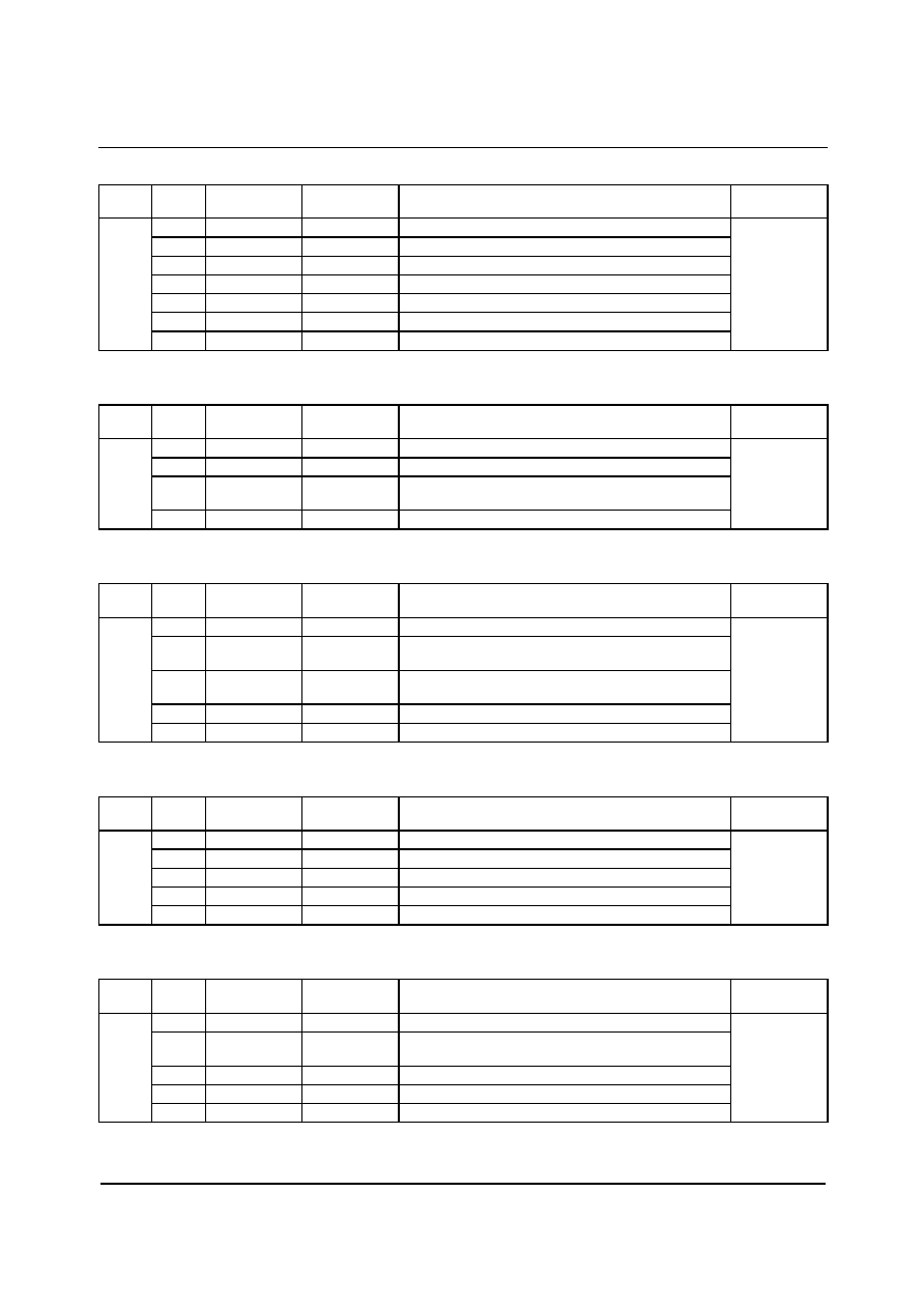
Production Data
WM9712L
w
PD Rev 4.0 December 2003
65
Register 12h controls the output signal of the auxiliary DAC.
REG
ADDR
BIT
LABEL
DEFAULT
DESCRIPTION
REFER TO
15
A2H
1 (mute)
Mutes AUXDAC to headphone mixer path
14:12
A2HVOL
010 (0dB)
Controls gain of AUXDAC to headphone mixer path
11
A2S
1 (mute)
Mutes AUXDAC to speaker mixer path
10:8
A2SVOL
010 (0dB)
Controls gain of AUXDAC to speaker mixer path
7
A2P
1 (mute)
Mutes AUXDAC to phone mixer path
6:4
A2PVOL
010 (0dB)
Controls gain of AUXDAC to phone mixer path
12h
0
AXE
0 (0FF)
Enables AUXDAC
Auxiliary DAC
Register 14h controls the side tone paths.
REG
ADDR
BIT
LABEL
DEFAULT
DESCRIPTION
REFER TO
15
STM
1 (mute)
Mutes microphone to headphone mixer path
14:12
STVOL
010 (0dB)
Controls gain of microphone to headphone mixer path
11:10
ALCM
11 (mute both)
Selects ALC to headphone mixer path. 00=stereo,
01=right only, 10=left only, 11=mute both left and right
14h
9:7
ALCVOL
010 (0dB)
Controls gain of ALC to headphone mixer path
Audio Mixers,
Side Tone
Control
Register 16h controls the analogue output pin OUT3, and also contains one control bit that affects LOUT2 and ROUT2.
REG
ADDR
BIT
LABEL
DEFAULT
DESCRIPTION
REFER TO
15
MU
1 (mute)
Mutes OUT3.
10:9
OUT3SRC
00 (-HPOUTL)
Selects source of OUT3 signal. 00=-HPOUTL, 01=VREF,
10=HPOUTL+HPOUTR, 11=-MONOOUT
8
SRC
0 (spkr mix)
Selects source of LOUT2 and ROUT2 signals. 0=from
speaker mixer, 1=from headphone mixer
7
ZC
0 (disabled)
Zero-cross enable
16h
5:0
OUT3VOL
000000 (0dB)
OUT3 volume
Analogue
Audio Outputs
Register 18h controls the audio DACs (but not AUXDAC).
REG
ADDR
BIT
LABEL
DEFAULT
DESCRIPTION
REFER TO
15
D2H
1 (mute)
Mutes DAC to headphone mixer path
14
D2S
1 (mute)
Mutes DAC to speaker mixer path
13
D2P
1 (mute)
Mutes DAC to phone mixer path
12:8
LDACVOL
01000 (0dB)
Controls left DAC input gain to all mixers
18h
4:0
RDACVOL
01000 (0dB)
Controls right DAC input gain to all mixers
Audio DACs
Register 1Ah controls the record selector and the ADC to phone mixer path.
REG
ADDR
BIT
LABEL
DEFAULT
DESCRIPTION
REFER TO
14
BOOST
0 (OFF)
Enables 20dB gain boost for recording
13:12
R2P
11 (mute)
Controls ADC to phone mixer path. 00=stereo, 01=left
ADC only, 10=right ADC only, 11=mute left and right
11
R2PBST
0 (OFF)
Enables 20dB gain boost for ADC to phone mixer path
10:8
RECSL
000 (mic)
Selects left ADC signal source
1Ah
2:0
RECSR
000 (mic)
Selects right ADC signal source
Audio ADC,
Record
Selector
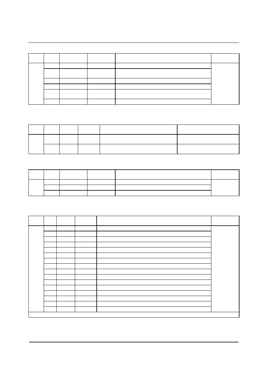
WM9712L
Production Data
w
PD Rev 4.0 December 2003
66
Register 1Ch controls the.recording gain.
REG
ADDR
BIT
LABEL
DEFAULT
DESCRIPTION
REFER TO
15
RMU
1 (mute)
Mutes audio ADC input
14
GRL
0 (standard)
Selects gain range for PGA of left ADC. 0=0...+22.5dB in
1.5dB steps, 1=-17.25...+30dB in 0.75dB steps
13:8
RECVOLL
000000 (0dB)
Controls left ADC recording volume
7
ZC
0 (OFF)
Enables zero-cross detector
6
GRR
0 (standard)
Selects gain range for PGA of left ADC. 0=0...+22.5dB in
1.5dB steps, 1=-17.25...+30dB in 0.75dB steps
1Ch
5:0
RECVOLR
000000 (0dB)
Controls right ADC recording volume
Audio ADC,
Record Gain
Register 20h is a "general purpose" register as defined by the AC'97 specification. Only two bits are implemented in the
WM9712L.
REG
ADDR
BIT
LABEL
DEFAULT
DESCRIPTION
REFER TO
13
3DE
0 (OFF)
Enables 3D enhancement
Audio DACs, 3D Stereo
Enhancement
20h
7
LB
0 (OFF)
Enables loopback (i.e. feed ADC output data
directly into DAC)
Intel's AC'97 Component
Specification, Revision 2.2, page 55
Register 22h controls 3D stereo enhancement for the audio DACs.
REG
ADDR
BIT
LABEL
DEFAULT
DESCRIPTION
REFER TO
5
3DLC
0 (low)
Selects lower cut-off frequency
4
3DUC
0 (high)
Selects upper cut-off frequency
22h
3:0
3DDEPTH
0000 (0%)
Controls depth of 3D effect
Audio DACs,
3D Stereo
Enhancement
Register 24h is for power management additional to the AC'97 specification. Note that the actual state of each circuit block
depends on both register 24h AND register 26h.
REG
ADDR
BIT
LABEL
DEFAULT
DESCRIPTION
REFER TO
15
PD15
0 *
Disables Crystal Oscillator
14
PD14
0 *
Disables left audio DAC
13
PD13
0 *
Disables right audio DAC
12
PD12
0 *
Disables left audio ADC
11
PD11
0 *
Disables right audio ADC
10
PD10
0 *
Disables MICBIAS
9
PD9
0 *
Disables left headphone mixer
8
PD8
0 *
Disables right headphone mixer
7
PD7
0 *
Disables speaker mixer
6
PD6
0 *
Disables MONO_OUT buffer (pin 33) and phone mixer
5
PD5
0 *
Disables OUT3 buffer (pin 37)
4
PD4
0 *
Disables headphone buffers (HPOUTL/R)
3
PD3
0 *
Disables speaker outputs (LOUT2, ROUT2)
2
PD2
0 *
Disables Line Input PGA (left and right)
1
PD1
0 *
Disables Phone Input PGA
24h
0
PD0
0 *
Disables Mic Input PGA (left and right)
Power
Management
* "0" corresponds to "ON", if and only if the corresponding bit in register 26h is also 0.
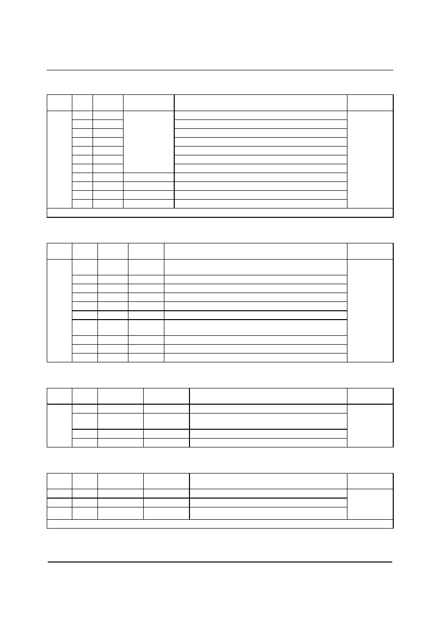
Production Data
WM9712L
w
PD Rev 4.0 December 2003
67
Register 26h is for power management according to the AC'97 specification. Note that the actual state of many circuit
blocks depends on both register 24h AND register 26h.
REG
ADDR
BIT
LABEL
DEFAULT
DESCRIPTION
REFER TO
14
PR6
Disables HPOUTL, HPOUTR and OUT3 Buffer
13
PR5
Disables Internal Clock
12
PR4
Disables AC-link interface (external clock off)
11
PR3
Disables VREF, analogue mixers and outputs
10
PR2
Disables analogue mixers, LOUT2, ROUT2 (but not VREF)
9
PR1
Disables Stereo DAC and AUXDAC
8
PR0
see note
Disables audio ADCs and input Mux
3
REF
inverse of PR2
Read-only bit, Indicates VREF is ready
2
ANL
inverse of PR3
Read-only bit, indicates analogue mixers are ready
1
DAC
inverse of PR1
Read-only bit, indicates audio DACs are ready
0
ADC
inverse of PR0
Read-only bit, indicates audio ADCs are ready
Power
Management
Note: PR6 to PR0 default to 1 if pin 47 is held high during reset, otherwise they default to 0.
Register 28h is a read-only register that indicates to the driver which advanced AC'97 features the WM9712L supports.
REG
ADDR
BIT
LABEL
DEFAULT
DESCRIPTION
REFER TO
15:14
ID
00
Indicates that the WM9712L is configured as the primary codec in
the system.
11:10
REV
01
Indicates that the WM9712L conforms to AC'97 Rev2.2
9
AMAP
0
Indicates that the WM9712L does not support slot mapping
8
LDAC
0
Indicates that the WM9712L does not have an LFE DAC
7
SDAC
0
Indicates that the WM9712L does not have Surround DACs
6
CDAC
0
Indicates that the WM9712L does not have a Centre DAC
3
VRM
0
Indicates that the WM9712L does not have a dedicated, variable
rate microphone ADC
2
SPDIF
1
Indicates that the WM9712L supports SPDIF output
1
DRA
0
Indicates that the WM9712L does not support double rate audio
28h
0
VRA
1
Indicates that the WM9712L supports variable rate audio
Intel's AC'97
Component
Specification,
Revision 2.2,
page 59
Register 2Ah controls the SPDIF output and variable rate audio.
REG
ADDR
BIT
LABEL
DEFAULT
DESCRIPTION
REFER TO
10
SPCV
1 (valid)
SPDIF validity bit (read-only)
5:4
SPSA
01 (slots 6, 9)
Controls SPDIF slot assignment. 00=slots 3 and 4,
01=6/9, 10=7/8, 11=10/11
2
SEN
0 (OFF)
Enables SPDIF output enable
2Ah
0
VRA
0 (OFF)
Enables variable rate audio
Digital Audio
(SPDIF)
Output
Registers 2Ch, 2Eh 32h and control the sample rates for the stereo DAC, auxiliary DAC and audio ADC, respectively.
REG
ADDR
BIT
LABEL
DEFAULT
DESCRIPTION
REFER TO
2Ch
all
DACSR
BB80h
Controls stereo DAC sample rate
2Eh
all
AUXDACSR
BB80h
Controls auxiliary DAC sample rate
32h
all
ADCSR
BB80h
Controls audio ADC sample rate
Variable Rate
Audio /
Sample Rate
Conversion
Note: The VRA bit in register 2Ah must be set first to obtain sample rates other than 48kHz
WM9712L
Production Data
w
PD Rev 4.0 December 2003
68
Register 3Ah controls the SPDIF output.
REG
ADDR
BIT
LABEL
DEFAULT
DESCRIPTION
REFER TO
15
V
0
Validity bit; `0' indicates frame valid, `1' indicates frame not
valid
14
DRS
0
Indicates that the WM9712L does not support double rate
SPDIF output (read-only)
13:12
SPSR
10
Indicates that the WM9712L only supports 48kHz
sampling on the SPDIF output (read-only)
11
L
0
Generation level; programmed as required by user
10:4
CC
0000000
Category code; programmed as required by user
3
PRE
0
Pre-emphasis; `0' indicates no pre-emphasis, `1' indicates
50/15us pre-emphasis
2
COPY
0
Copyright; `0' indicates copyright is not asserted, `1'
indicates copyright
1
AUDIB
0
Non-audio; `0' indicates data is PCM, `1' indicates non-
PCM format (e.g. DD or DTS)
3Ah
0
PRO
0
Professional; `0' indicates consumer, `1' indicates
professional
Digital Audio
(SPDIF)
Output
Register 4Ch to 54h control the GPIO pins and virtual GPIO signals.
REG
ADDR
BIT
LABEL
DEFAULT
DESCRIPTION
REFER TO
4Ch
all 1 (all inputs)
except unused
bits
Controls GPIO configuration as inputs or as outputs (note:
virtual GPIOs can only be inputs)
4Eh
all 1
Controls GPIO polarity (actual polarity depends on register
4Ch AND register 4Eh)
50h
all 0 (not sticky)
Makes GPIO signals sticky
52h
all 0 (OFF)
Enables wake-up for each GPIO signal
54h
= status of GPIO
inputs
GPIO pin status (read from inputs, write `0' to clear sticky bits)
15
Controls Comparator 1 signal (virtual GPIO)
14
Controls Comparator 2 signal (virtual GPIO)
13
Controls Pen-Down Detector signal (virtual GPIO)
12
Controls ADA signal (virtual GPIO)
11
Controls Thermal sensor signal (virtual GPIO)
10-6
Unused
5
Controls GPIO5 (pin 48)
4
Controls GPIO4 (pin 47)
3
Controls GPIO3 (pin 46)
2
Controls GPIO2 (pin 45)
1
please
refer to
the
register
map
Controls GPIO1 (pin 44)
GPIO and
Interrupt
Control
Register 56h controls the use of GPIO pins for non-GPIO functions.
REG
ADDR
BIT
LABEL
DEFAULT
DESCRIPTION
REFER TO
5
GE5
1 (GPIO)
Selects between GPIO5 and SPDIF_OUT function for pin 48
4
GE4
1 (GPIO)
Selects between GPIO4 and ADA/MASK functionS for pin 47
3
GE3
1 (GPIO)
Selects between GPIO3 and PENDOWN function for pin 46
56h
2
GE2
1 (GPIO)
Selects between GPIO2 and IRQ function for pin 45
GPIO and
Interrupt
Control
Production Data
WM9712L
w
PD Rev 4.0 December 2003
69
Register 58h controls several additional functions.
REG
ADDR
BIT
LABEL
DEFAULT
DESCRIPTION
REFER TO
15:13
COMP2DEL
000 (no delay)
Selects Comparator 2 delay
Battery Alarm
12
JIEN
0
Enables Jack Insert Detection
11
FRC
0
Forces Jack Insert Detection
Analogue Audio Outputs, Jack
Insertion and Auto-Switching
10
SVD
0 (enabled)
Disables VREF for lowest possible power
consumption
Power Management
3:2
DIE REV
Indicates device revision. 00=Rev.A, 01=Rev.B, 10=Rev.C
N/A
1
WAKEEN
0 (no wake-up)
Enables GPIO wake-up
58h
0
IRQ INV
0 (not inverted)
Inverts the IRQ signal (pin 45)
GPIO and Interrupt Control
Register 5Ch controls several additional functions.
REG
ADDR
BIT
LABEL
DEFAULT
DESCRIPTION
REFER TO
15
AMUTE
0
Read-only bit to indicate DAC auto-muting
Audio DACs, Stereo DACs
14
C1REF
0 (AVDD/2)
Selects Comparator 1 Reference Voltage
13:12
C1SRC
00 (OFF)
Selects Comparator 1 Signal Source
11
C2REF
0 (AVDD/2)
Selects Comparator 1 Reference Voltage
10:9
C2SRC
00 (OFF)
Selects Comparator 1 Signal Source
Battery Alarm
8
DS
0
Selects differential microphone input pins. 0=MIC1
and MIC2, 1=LINEL and LINER
Analogue Inputs,
Microphone Input
7
AMEN
0 (OFF)
Enables DAC Auto-Mute
6:5
VBIAS
00
Selects analogue bias for lowest power, depending
on AVDD supply. 0X=3.3V, 10=2.5V, 11=1.8V
Power Management
4
ADCO
0
Selects source of SPDIF data. 0=from SDATAOUT,
1= from audio ADC
Digital Audio (SPDIF)
Output
3
HPF
0
Disables ADC high-pass filter
Audio ADC
2
ENT
0
Enables thermal sensor
Analogue Audio Outputs,
Thermal Sensor
5Ch
1:0
ASS
00
Selects time slots for stereo ADC data. 00=slots 3
and 4, 01=7/8, 10=6/9, 11=10/11
Audio ADC, ADC Slot
Mapping
Registers 60h and 62h control the ALC and Noise Gate functions.
REG
ADDR
BIT
LABEL
DEFAULT
DESCRIPTION
REFER TO
15:12
ALCL
1011 (-12dB)
Controls ALC threshold
11:8
HLD
0000 (0 ms)
Controls ALC hold time
7:4
DCY
0011 (192 ms)
Controls ALC decay time
60h
3:0
ATK
0010 (24 ms)
Controls ALC attack time
15:14
ALCSEL
00 (OFF)
Controls which channel ALC operates on. 00=none,
01=right only, 10=left only, 11=both
13:11
MAXGAIN
111 (+30dB)
Controls upper gain limit for ALC
10:9
ZC TIMEOUT
11 (slowest)
Controls time-out for zero-cross detection
8
ALCZC
0 (OFF)
Enables zero-cross detection for ALC
7
NGAT
0 (OFF)
Enables noise gate function
5
NGG
0 (hold gain)
Selects noise gate type. 0=hold gain, 1=mute
62h
4:0
NGTH
00000 (-76.5dB)
Controls noise gate threshold
Audio ADC,
Automatic
Level Control

WM9712L
Production Data
w
PD Rev 4.0 December 2003
70
Register 64h controls the input signal of the auxiliary DAC.
REG
ADDR
BIT
LABEL
DEFAULT
DESCRIPTION
REFER TO
15
XSLE
0
Selects input for AUXDAC. 0=from AUXDACVAL (for DC
signals), 1=from AC-Link slot (for AC signals)
14:12
AUXDACSLT
000 (Slot 5)
Selects input slot for AUXDAC (with XSLE=1)
64h
11:0
AUXDACVAL
000000000
AUXDAC Digital Input for AUXDAC (with XSLE=0). 000h=
minimum, FFFh=full-scale
Auxiliary DAC
Registers 76h, 78h and 7Ah control the touchpanel interface.
REG
ADDR
BIT
LABEL
DEFAULT
DESCRIPTION
REFER TO
15
POLL
0
Writing "1" starts a measurement (this bit resets itself)
14:12
ADCSEL
000 (none)
Selects measurement type
11
COO
0 (OFF)
Enables co-ordinate mode
10
CTC
0 (polling)
Enables continuous conversions
9:8
CR
00 (93.75Hz)
Controls conversion rate in continuous mode
7:4
DEL
0000 (20.8
µ
s)
Controls touchpanel settling time
3
SLEN
1
Enables slot readback of touchpanel data
76h
2:0
SLT
10
Selects time slot for readback of touchpanel data
15:14
PRP
00
Selects mode of operation. 00=OFF, 01=pen detect with
wake-up, 10=pen detect without wake-up, 11=running
13
RPR
0
Selects wake-up mode. 0=AC-Link only, 1=AC-Link and
WM9712L auto-wake-up
12
45W
0 (4-wire)
Selects 4-wire or 5-wire touchpanel
11
PDEN
0 (always)
Selects when touchpanel measurements take place.
0=always, 1=only when pen is down
9
WAIT
0
Controls data readback from register 7Ah. 0=overwrite old
data with new, 1=wait until old data has been read
8
PIL
0 (200
µ
A)
Controls current used for pressure measurement. 1=400
µ
A
7:6
MSK
00 (OFF)
Controls MASK feature
78h
5:0
RPU
000001 (64k
)
Controls internal pull-up resistor for pen-down detection
15
PNDN
0 (pen up)
Indicates pen status.
14:12
ADCSRC
000 (none)
Indicates measurement type
7Ah
read
only
11:0
ADCD
000h
Returns data from touchpanel / AUXADC
Touchpanel
Interface
Register 7Ch and 7Eh are read-only registers that indicate to the driver that the codec is a WM9712L.
REG
ADDR
BIT
LABEL
DEFAULT
DESCRIPTION
REFER TO
15:8
F7:0
57h
ASCII character "W" for Wolfson
7Ch
7:0
S7:0
4Dh
ASCII character "M"
15:8
T7:0
4Ch
ASCII character "L"
7Eh
7:0
REV7:0
12h
12 for WM9712L
Intel's AC'97
Component
Specification,
Revision 2.2,
page 50
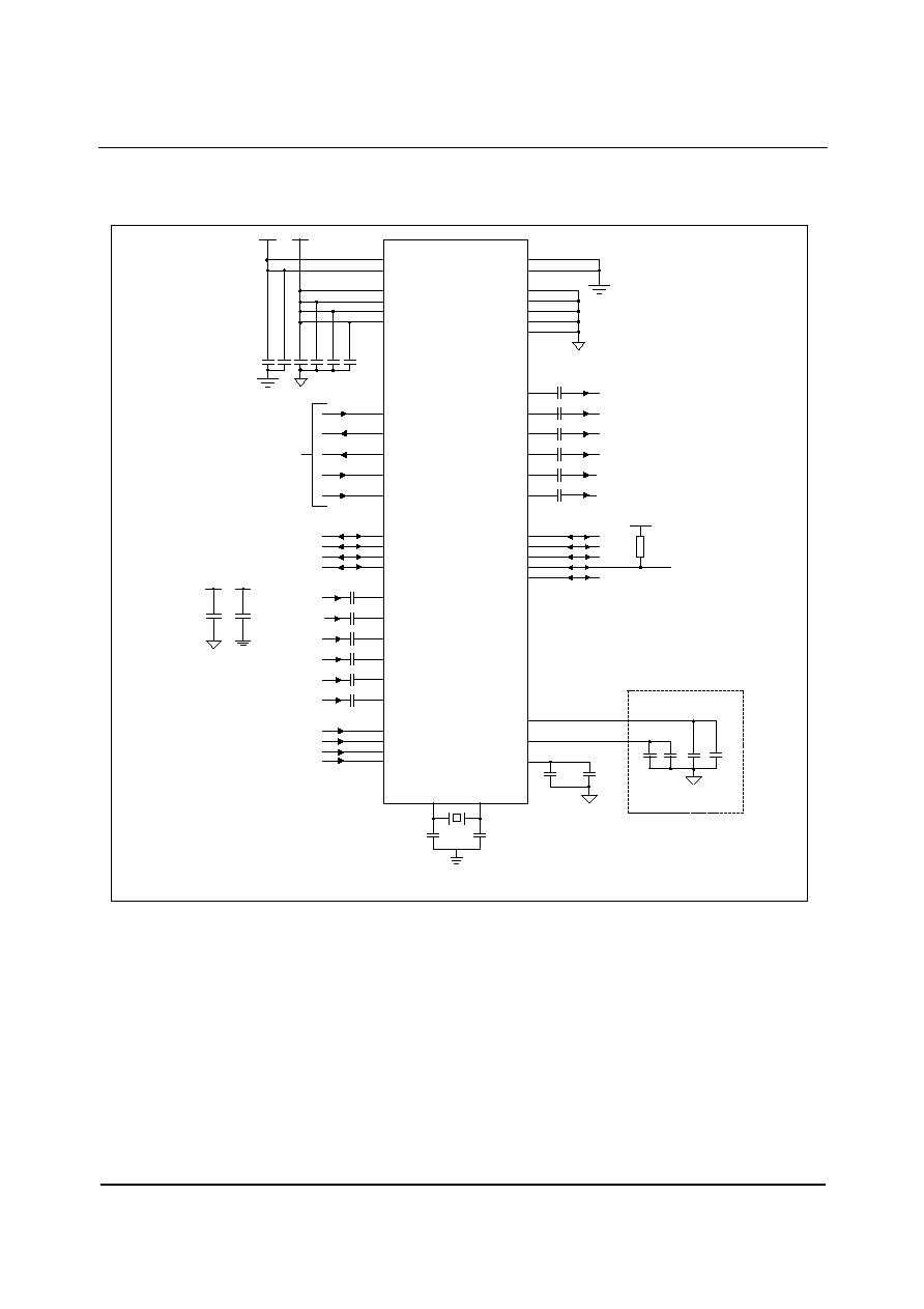
Production Data
WM9712L
w
PD Rev 4.0 December 2003
71
APPLICATIONS INFORMATION
RECOMMENDED EXTERNAL COMPONENTS
1
9
25
38
DBVDD
DCVDD
AVDD
TPVDD
PCBEEP
19
PHONE
20
X+/BR
14
Y+/TR
15
X-/TL
16
Y-/BL
17
MIC1
21
MIC2
22
LINEINL
23
LINEINR
24
SDATAOUT
BITCLK
6
SDATAIN
8
SYNC
10
RESETB
11
AC-
LINK
XTLOUT
3
XTLIN
GND
XT
4
7
DGND2
DGND1
AGND
26
AGND2
34
SPKGND
40
LOUT2
35
ROUT2
36
OUT3
HPOUTL
39
HPOUTR
41
GPIO1
44
GPIO2/IRQ
45
GPIO3/PENDOWN
46
GPIO4/ADA/MASK
47
GPIO5/SPDIF_OUT
48
MICBIAS
28
VREF
27
CAP2
32
2
WM9712L
AGND
+
+
+
+
AGND
+
AGND
+
C15
C27
C28
C9
C12
C13
C14
C10
C16
C17
C18
C19
C20
+
C11
C25
C26
C22
C23
5
SPKVDD
HPVDD
GND
AGND
GND
HPGND
TPGND
18
42
43
13
COMP1/AUX1
WIPER/AUX4
BMON/AUX3
COMP2/AUX2
12
31
30
29
MONOOUT
33
+
C21
C6
C5
C4
C3
C2
C1
Layout
Notes:
1. C1 to C6, C9 C11 and C13 should be as close to
the relative WM9712L connecting pin as possible.
2. AGND and DGND should be connected as close
to the WM9712L as possible.
37
+
C24
DVDD
AVDD
See External Components
Descriptions for details
C8
DVDD
+
GND
C7
+
AGND
AVDD
R1
DBVDD
Figure 23 External Components Diagram
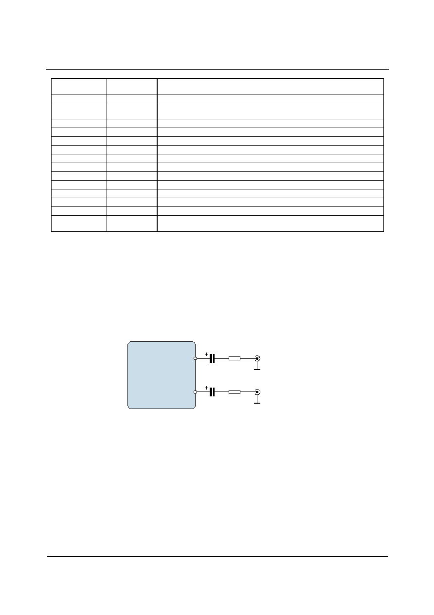
WM9712L
Production Data
w
PD Rev 4.0 December 2003
72
COMPONENT
REFERENCE
SUGGESTED
VALUE
DESCRIPTION
C1 - C6
100nF
De-coupling for DBVDD,DCVDD,TPVDD,AVDD,SPKVDD,HPVDD
C7 - C8
10uF
Reservoir capacitor for DVDD, AVDD. Should the supplies use separate sources then
additional capacitors will be required of each additional source.
C9
100nF
De-coupling for CAP2.
C10
10uF
Reservoir capacitor for CAP2
C11
100nF
De-coupling for VREF
C12
10uF
Reservoir capacitor for VREF
C13
100nF
De-coupling for MICBIAS - Not required if MICBIAS output is not used
C14
10uF
Reservoir capacitor for MICBIAS - Not required if MICBIAS output is not used
C27 & C28
22pF
Required when used with a parallel resonant crystal.
C15 - C20
1uF
AC coupling capacitors
C21 - C23
2.2uF
Output AC coupling capacitors to remove VREF DC level from outputs
C24 - C26
220
µ
F
Output AC coupling capacitors to remove VREF DC level from outputs.
R1
100k
Pull-up resistor, ensures that all circuit blocks are OFF by default
XT
24.576MHz
AC'97 master clock frequency. A bias resistor is not required but if connected will not
affect operation if the value is large (above 1M
)
Table 46 External Components Descriptions
Note:
1. For Capacitors C7, C8, C10, C12 and C14 it is recommended that very low ESR components are used.
LINE OUTPUT
The headphone outputs, HPOUTL and HPOUTR, can be used as stereo line outputs. The speaker
outputs, LOUT2 and ROUT2, can also be used as line outputs, if LOUT2 is not inverted for BTL
operation (INV = 0). Recommended external components are shown below.
HPGND
HPGND
LINE-OUT
SOCKET
(LEFT)
C1
1uF
R1
100 Ohm
HPOUTL /
LOUT2
HPOUTR /
ROUT2
WM9712L
R2
100 Ohm
LINE-OUT
SOCKET
(RIGHT)
C2
1uF
Figure 24 Recommended Circuit for Line Output
The DC blocking capacitors and the load resistance together determine the lower cut-off frequency,
fc. Assuming a 10 k
load and C1, C2 = 10
µ
F:
fc = 1 / 2
(R
L
+R
1
) C
1
= 1 / (2
x 10.1k
x 1
µ
F) = 16 Hz
Increasing the capacitance lowers fc, improving the bass response. Smaller values of C1 and C2 will
diminish the bass response. The function of R1 and R2 is to protect the line outputs from damage
when used improperly.
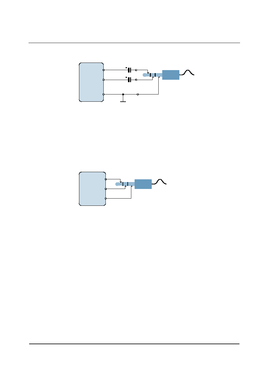
Production Data
WM9712L
w
PD Rev 4.0 December 2003
73
AC-COUPLED HEADPHONE OUTPUT
The circuit diagram below shows how to connect a stereo headphone to the WM9712L.
C2 220uF
HPOUTL
HPOUTR
HPGND = 0V
C1 220uF
WM9712L
Figure 25 Simple Headphone Output Circuit Diagram
The DC blocking capacitors C1 and C2 together with the load resistance determine the lower cut-off
frequency, fc. Increasing the capacitance lowers fc, improving the bass response. Smaller
capacitance values will diminish the bass response. For example, with a 16
load and C1 = 220
µ
F:
fc = 1 / 2
R
L
C
1
= 1 / (2
x 16
x 220
µ
F) = 45 Hz
DC COUPLED (CAPLESS) HEADPHONE OUTPUT
In the interest of saving board space and cost, it may be desirable to eliminate the 220
µ
F DC
blocking capacitors. This can be achieved by using OUT3 as a headphone pseudo-ground, as shown
below.
WM9712L
HPOUTL
HPOUTR
OUT3 = AVDD/2
Figure 26 Capless Headphone Output Circuit Diagram (OUT3SRC = 10)
As the OUT3 pin produces a DC voltage of AVDD/2, there is no DC offset between
HPOUTL/HPOUTR and OUT3, and therefore no DC blocking capacitors are required. However, this
configuration has some drawbacks:
∑
The power consumption of the WM9712L is increased, due to the additional power
consumed in the OUT3 output buffer.
∑
If the DC coupled output is connected to the line-in of a grounded piece of equipment,
then OUT3 becomes short-circuited. Although the built-in short circuit protection will
prevent any damage to the WM9712L, the audio signal will not be transmitted properly.
∑
OUT3 cannot be used for another purpose
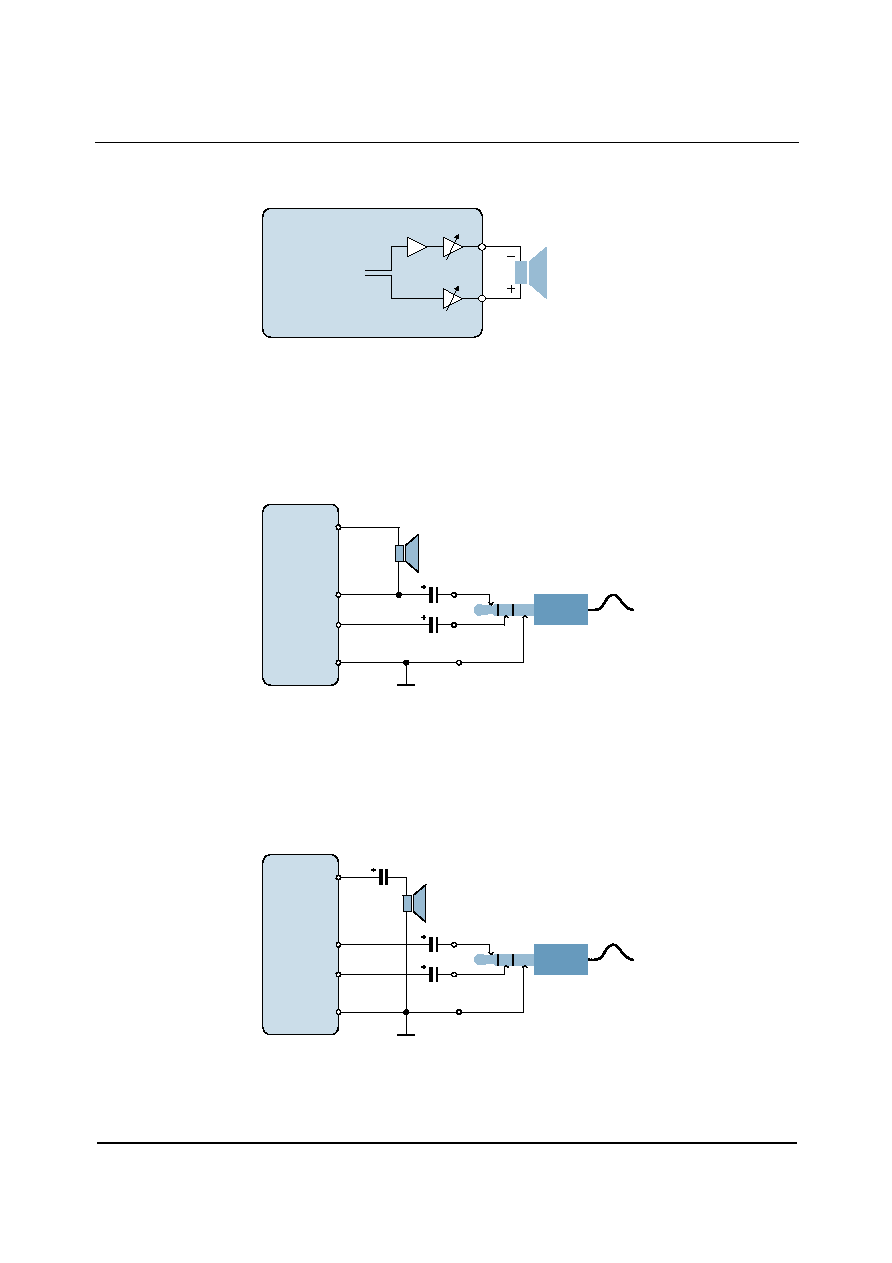
WM9712L
Production Data
w
PD Rev 4.0 December 2003
74
BTL LOUDSPEAKER OUTPUT
LOUT2 and ROUT2 can differentially drive a mono 8
loudspeaker as shown below.
LOUT2
ROUT2
WM9712L
INV = 1
Stereo: V
SPKR
= R-(-L) = L+R
Mono: V
SPKR
= M-(-M) = 2M
ROUT2VOL
LOUT2VOL
-1
Figure 27 Speaker Output Connection (INV = 1)
The right channel is inverted by setting the INV bit, so that the signal across the loudspeaker is the
sum of left and right channels.
COMBINED HEADSET / BTL EAR SPEAKER
In smartphone applications with a loudspeaker and separate ear speaker (receiver), a BTL ear
speaker can be connected at the OUT3 pin, as shown below.
HPOUTL
HPOUTR
HPGND = 0V
WM9712L
OUT3
BTL ear
speaker
Figure 28 Combined Headset / BTL Ear Speaker (OUT3SRC = 00)
The ear speaker and the headset play the same signal. Whenever the headset is plugged in, the
headphone outputs are enabled and OUT3 disabled. When the headset is not plugged in, OUT3 is
enabled (see "Jack Insertion and Auto-Switching")
COMBINED HEADSET / SINGLE-ENDED EAR SPEAKER
Instead of a BTL ear speaker, a single-ended ear speaker can also be used, as shown below.
HPOUTL
HPOUTR
HPGND = 0V
WM9712L
OUT3
ear speaker
(single-ended)
Figure 29 Combined Headset / Single-ended Ear Speaker (OUT3SRC = 01)
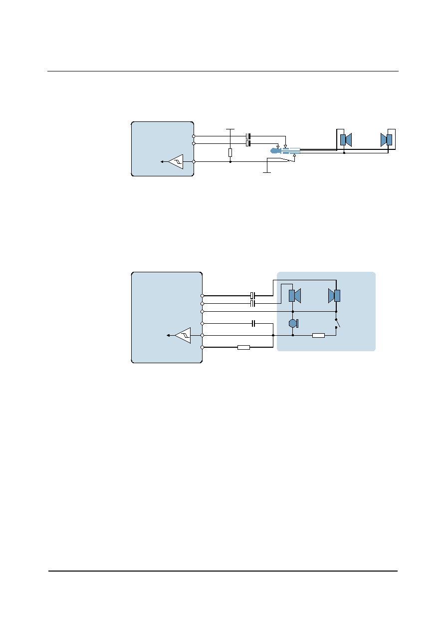
Production Data
WM9712L
w
PD Rev 4.0 December 2003
75
JACK INSERT DETECTION
The circuit diagram below shows how to detect when a headphone or headset has been plugged into
the headphone socket. It generates an interrupt, instructing the controller to enable HPOUTL and
HPOUTR and disable OUT3.
L
R
switch closes
on insertion
+
-
+
-
HPOUTL
HPOUTR
GPIO
interrupt
logic
100k
DBVDD
Figure 30 Jack Insert Detection Circuit
The circuit requires a headphone socket with a switch that closes on insertion. It detects both
headphones and phone headsets. Any GPIO pin can be used, provided that it is configured as an
input.
HOOKSWITCH DETECTION
The circuit diagram below shows how to detect when the "hookswitch" of a phone headset is pressed
(pressing the hookswitch is equivalent to lifting the receiver in a stationary telephone).
GPIO
interrupt
logic
MIC
L
R
HOOK
SWITCH
47
+
-
+
-
HPOUTL
HPOUTR
MICL/MICR
AGND
680
-
2.2k
MICBIAS
PHONE HEADSET
WM9712L
Figure 31 Hookswitch Detection Circuit
The circuit uses a GPIO pin as a sense input. The impedance of the microphone and the resistor in
the MICBIAS path must be such that the potential at the GPIO pin is above 0.7
◊
DBVDD when the
hookswitch is open, and below 0.3
◊
DBVDD when it is closed.
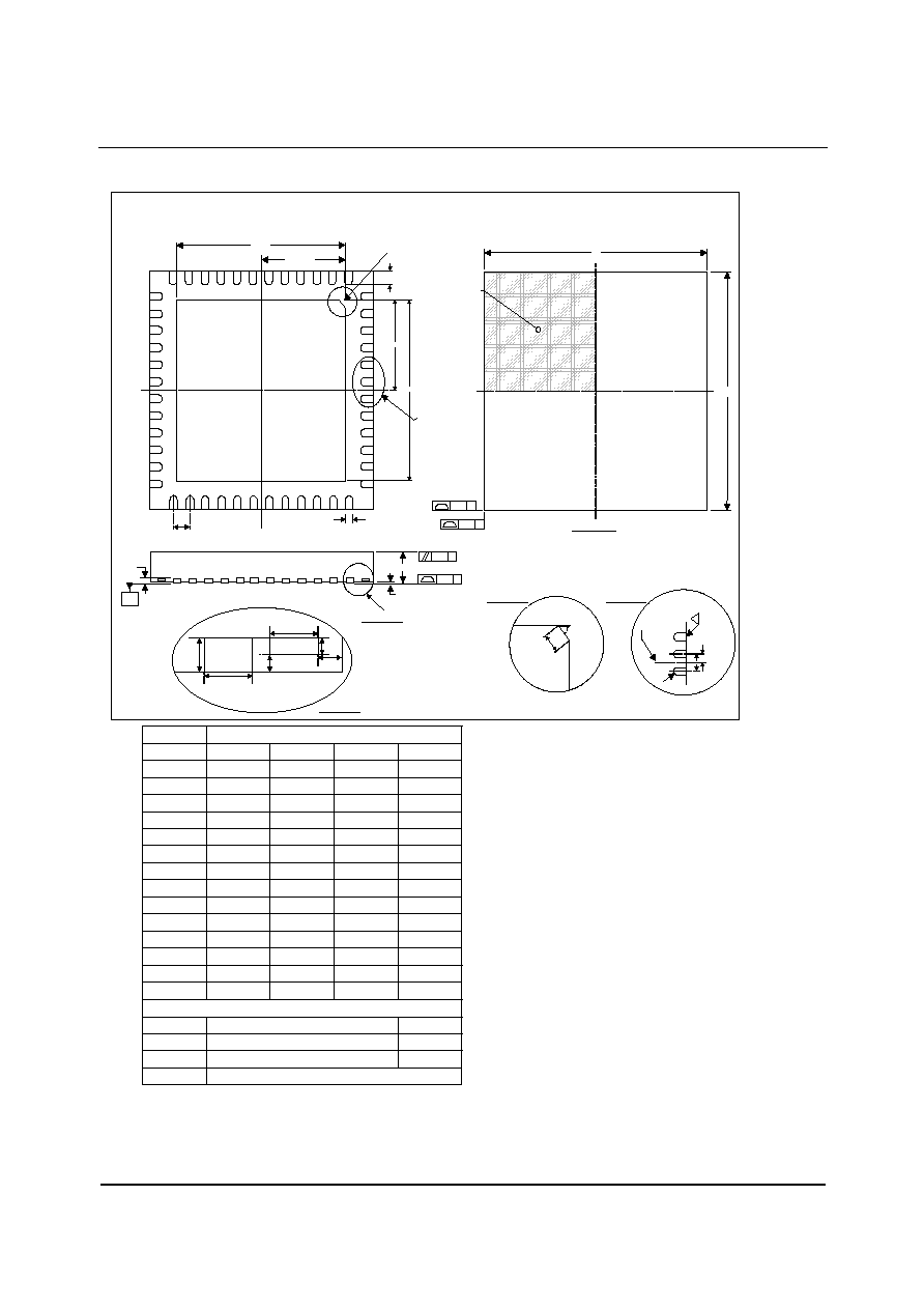
WM9712L
Production Data
w
PD Rev 4.0 December 2003
76
PACKAGE DRAWING - QFN
e
DM029.C
FL: 48 PIN QFN PLASTIC PACKAGE 7
X
7
X
0.9 mm BODY, 0.50 mm LEAD PITCH
INDEX AREA
(D/2 X E/2)
TOP VIEW
C
aaa
2 X
SEE DETAIL 2
E2
E2/2
b
D2
24
L
D2/2
C
aaa
2 X
25
36
37
48
1
12
13
D
E
e
Datum
SEE DETAIL 1
C
0.08
C
ccc
A
A1
C
(A3)
SEATING PLANE
DETAIL 3
DETAIL 3
DETAIL 2
Terminal
tip
R
e/2
1
DETAIL 1
0.35mm
45
degrees
(A3)
G
T
H
W
b
Exposed lead
Half etch tie bar
Symbols
Dimensions (mm)
MIN
NOM
MAX
NOTE
A
b
D
D2
E
E2
e
L
0.80
0.90
1.00
0.30
0.25
0.18
7.00 BSC
5.25
5.15
5.00
7.00 BSC
0.5 BSC
5.15
5.25
5.00
0.30
0.4
0.50
1
A1
A3
0
0.02
0.05
0.20 REF
G
H
0.213
0.1
NOTES:
1. DIMENSION b APPLIED TO METALLIZED TERMINAL AND IS MEASURED BETWEEN 0.15 mm AND 0.30 mm FROM TERMINAL TIP.
2. ALL DIMENSIONS ARE IN MILLIMETRES
3. THE TERMINAL #1 IDENTIFIER AND TERMINAL NUMBERING CONVENTION SHALL CONFORM TO JESD 95-1 SPP-002.
4. COPLANARITY APPLIES TO THE EXPOSED HEAT SINK SLUG AS WELL AS THE TERMINALS.
5. THIS DRAWING IS SUBJECT TO CHANGE WITHOUT NOTICE.
JEDEC, MO-220, VARIATION VKKD-2
Tolerances of Form and Position
T
W
aaa
bbb
ccc
0.1
0.2
0.15
0.10
0.10
REF
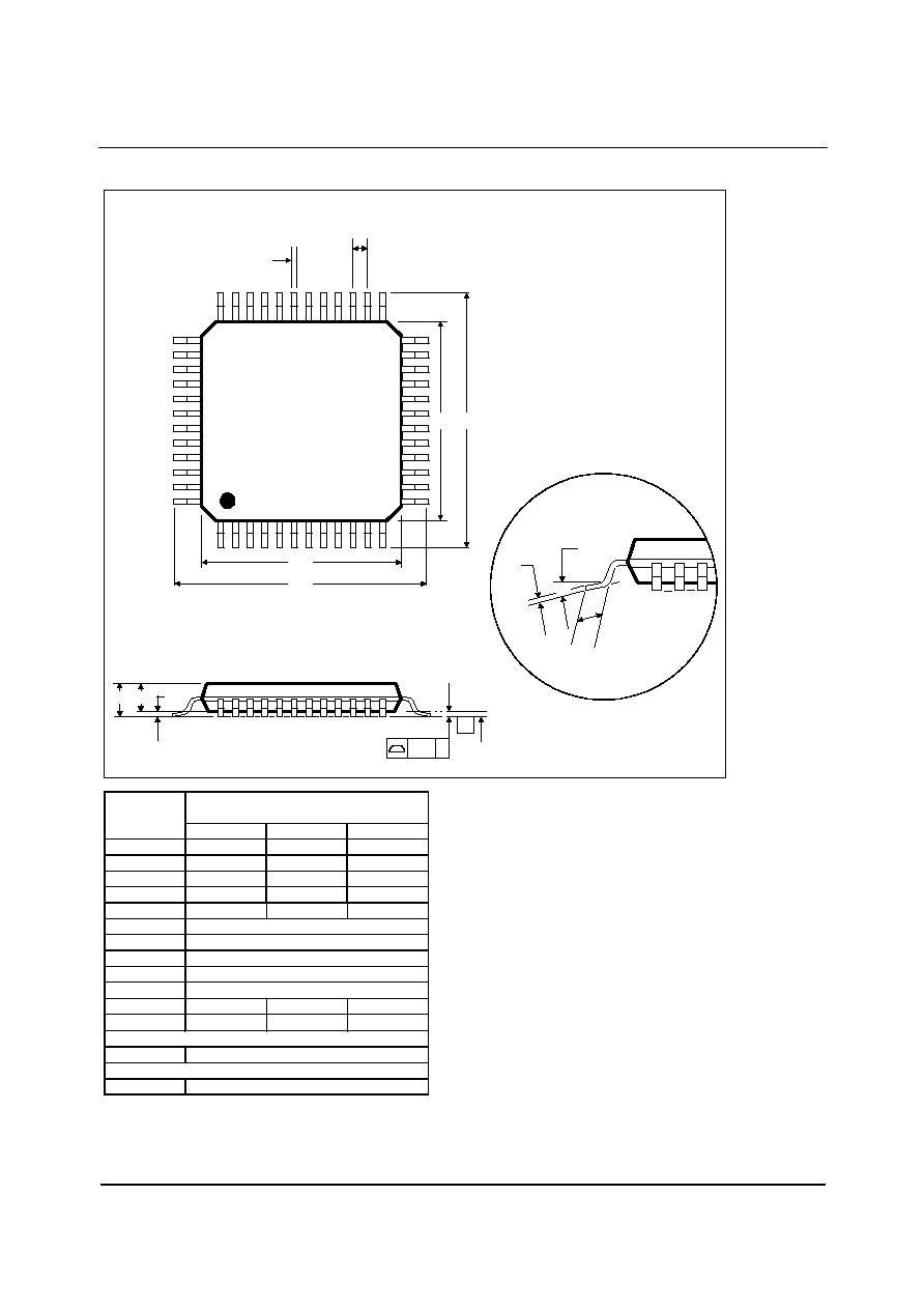
Production Data
WM9712L
w
PD Rev 4.0 December 2003
77
PACKAGE DRAWING ≠ TQFP
NOTES:
A. ALL LINEAR DIMENSIONS ARE IN MILLIMETERS.
B. THIS DRAWING IS SUBJECT TO CHANGE WITHOUT NOTICE.
C. BODY DIMENSIONS DO NOT INCLUDE MOLD FLASH OR PROTRUSION, NOT TO EXCEED 0.25MM.
D. MEETS JEDEC.95 MS-026, VARIATION = ABC. REFER TO THIS SPECIFICATION FOR FURTHER DETAILS.
DM004.C
FT: 48 PIN TQFP (7 x 7 x 1.0 mm)
Symbols
Dimensions
(mm)
MIN
NOM
MAX
A
-----
-----
1.20
A
1
0.05
-----
0.15
A
2
0.95
1.00
1.05
b
0.17
0.22
0.27
c
0.09
-----
0.20
D
9.00 BSC
D
1
7.00 BSC
E
9.00 BSC
E
1
7.00 BSC
e
0.50 BSC
L
0.45
0.60
0.75
0
o
3.5
o
7
o
Tolerances of Form and Position
ccc
0.08
REF:
JEDEC.95, MS-026
25
36
e
b
12
1
D1
D
E1
E
13
24
37
48
A
A2
A1
SEATING PLANE
ccc C
-C-
c
L

WM9712L
Production Data
w
PD Rev 4.0 December 2003
78
IMPORTANT NOTICE
Wolfson Microelectronics plc (WM) reserve the right to make changes to their products or to discontinue any product or
service without notice, and advise customers to obtain the latest version of relevant information to verify, before placing
orders, that information being relied on is current. All products are sold subject to the WM terms and conditions of sale
supplied at the time of order acknowledgement, including those pertaining to warranty, patent infringement, and limitation
of liability.
WM warrants performance of its products to the specifications applicable at the time of sale in accordance with WM's
standard warranty. Testing and other quality control techniques are utilised to the extent WM deems necessary to support
this warranty. Specific testing of all parameters of each device is not necessarily performed, except those mandated by
government requirements.
In order to minimise risks associated with customer applications, adequate design and operating safeguards must be used
by the customer to minimise inherent or procedural hazards. Wolfson products are not authorised for use as critical
components in life support devices or systems without the express written approval of an officer of the company. Life
support devices or systems are devices or systems that are intended for surgical implant into the body, or support or
sustain life, and whose failure to perform when properly used in accordance with instructions for use provided, can be
reasonably expected to result in a significant injury to the user. A critical component is any component of a life support
device or system whose failure to perform can be reasonably expected to cause the failure of the life support device or
system, or to affect its safety or effectiveness.
WM assumes no liability for applications assistance or customer product design. WM does not warrant or represent that
any license, either express or implied, is granted under any patent right, copyright, mask work right, or other intellectual
property right of WM covering or relating to any combination, machine, or process in which such products or services might
be or are used. WM's publication of information regarding any third party's products or services does not constitute WM's
approval, license, warranty or endorsement thereof.
Reproduction of information from the WM web site or datasheets is permissible only if reproduction is without alteration and
is accompanied by all associated warranties, conditions, limitations and notices. Representation or reproduction of this
information with alteration voids all warranties provided for an associated WM product or service, is an unfair and deceptive
business practice, and WM is not responsible nor liable for any such use.
Resale of WM's products or services with statements different from or beyond the parameters stated by WM for that
product or service voids all express and any implied warranties for the associated WM product or service, is an unfair and
deceptive business practice, and WM is not responsible nor liable for any such use.
ADDRESS:
Wolfson Microelectronics plc
20 Bernard Terrace
Edinburgh
EH8 9NX
United Kingdom
Tel :: +44 (0)131 272 7000
Fax :: +44 (0)131 272 7001
Email ::
sales@wolfsonmicro.com