Document Outline
- WM9705
- Multimedia AC'97 Codec with Integrated Touch Screen Controller
- DESCRIPTION
- FEATURES
- APPLICATIONS
- BLOCK DIAGRAM
- ORDERING INFORMATION
- ABSOLUTE MAXIMUM RATINGS
- RECOMMENDED OPERATING CONDITIONS
- PIN CONFIGURATION
- PIN DESCRIPTION
- ELECTRICAL CHARACTERISTICS
- POWER CONSUMPTION
- DETAILED TIMING DIAGRAMS
- AC-LINK LOW POWER MODE
- COLD RESET
- WARM RESET
- CLOCK SPECIFICATIONS
- DATA SETUP AND HOLD (50PF EXTERNAL LOAD)
- SIGNAL RISE AND FALL TIMES
- DEVICE DESCRIPTION
- INTRODUCTION
- ACê97 FEATURES
- NON - ACê97 FEATURES
- PEN DIGITIZER AND AUXILIARY ADC
- 3-D STEREO ENHANCEMENT
- VARIABLE SAMPLE RATE SUPPORT
- SPDIF OR I 2 S DIGITAL AUDIO DATA OUTPUT
- PRIMARY/SECONDARY ID SUPPORT
- HEADPHONE DRIVE AND HEADSET AUTODETECT
- DATA SLOT MAPPING
- AC-LINK DIGITAL SERIAL INTERFACE PROTOCOL
- AC-LINK AUDIO OUTPUT FRAME (SDATAOUT)
- AC-LINK AUDIO INPUT FRAME (SDATAIN)
- AC-LINK LOW POWER MODE
- WAKING UP THE AC-LINK
- SERIAL INTERFACE REGISTER MAP DESCRIPTION
- REGISTER 28h Ö EXTENDED AUDIO ID
- REGISTER 2AH Ö EXTENDED AUDIO STATUS AND CONTROL REGISTER
- REGISTER 2Ch AND 32h Ö AUDIO SAMPLE RATE CONTROL REGISTERS
- REGISTERS 3AH Ö SPDIF CONTROL REGISTER
- VENDOR SPECIFIC REGISTERS (INDEX 5Ah - 7Ah)
- SERIAL INTERFACE REGISTER MAP
- PEN DIGITISER OPERATION
- TIMING OF PEN DIGITISER OPERATIONS
- CONTROL OF PEN DIGITISER FUNCTIONS
- READBACK OF PEN DIGITISER RESULTS
- CONVERSION CONTROL
- PRESSURE MEASUREMENT
- MASK FUNCTION
- STANDBY OPERATION AND WAKE-UP
- AUXILIARY CONVERSIONS
- RECOMMENDED EXTERNAL COMPONENTS
- PACKAGE DIMENSIONS - TQFP
- PACKAGE DIMENSIONS - QFN
- IMPORTANT NOTICE
WM9705
Multimedia AC'97 Codec with
Integrated Touch Screen Controller
WOLFSON MICROELECTRONICS LTD
www.wolfsonmicro.com
Advance Information, October 2002, Rev 3.6
Copyright
2002 Wolfson Microelectronics Ltd
.
DESCRIPTION
The W M9705 is a high-quality stereo audio codec with an
integrated touch screen controller.
The audio section is compliant with the Intel AC'97 Rev 2.2
specification. It performs full-duplex 18-bit codec functions and
supports variable sample rates from 8 to 48k samples/s with high
signal to noise ratio. Optional AC'97 features include 3D sound
enhancement, line-level outputs, stereo buffered headphone
outputs, hardware sample rate conversion, primary/secondary
mode operation and S/PDIF output. Headphone auto-detect, I
2
S
output and headphone buffer on the mono output are included.
Additionally, the WM9705 integrates a complete 4-wire touch
screen controller, including on-chip screen drivers, pen-down
detection feature, and pressure measurement capability.
A 5-pin digital bi-directional AC-Link serial interface allows transfer
of control data and DAC and ADC words to and from the AC'97
controller. The WM9705 is fully operable on 3V or 5V or mixed
3/5V supplies, and is packaged in the industry standard 48-pin
TQFP package with 7mm body size, or in a smaller 7
◊
7
◊
0.9mm
QFN.
FEATURES
∑
AC'97 rev2.2 compliant codec with pen digitiser
∑
18-bit stereo audio codecs
∑
On-chip sample rate conversion
∑
Multiple channel input mixer
∑
S/PDIF digital audio output
∑
Headphone drivers on AUX and MONO outputs
∑
4-wire touch screen interface with co-ordinate and pressure
measurement, and pen-down detection
∑
Wake-up from sleep mode on pen down
∑
3V to 5V operation
∑
Extensive power management features including hardware
power down option
∑
Standard AC'97 pinout in 48-pin TQFP package or 48-pin
QFN package.
APPLICATIONS
∑
Personal Digital Assistants and `Smartphones'
∑
PocketPC
systems
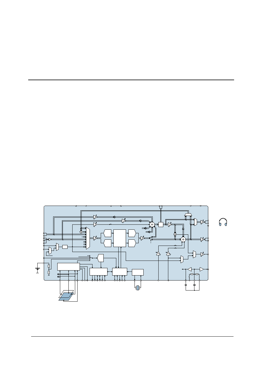
BLOCK DIAGRAM
ƒ
WM9705
DVDD1
DGND1
DAC
L
HPGND
HPVDD
HPGND
DAC
R
SD
ATAI
N
SYN
C
BI
TC
L
K
R
ESET
B
SD
A
T
AO
U
T
DIGITAL
FILTERS
MODULATION
VARIABLE
RATE AUDIO
Y+
/
V
I
D
L
X+
/
A
U
X
L
X-
/
A
U
X
R
Y-
/
V
I
D
R
PEN DOWN
AUXADC
TOUCH PANEL
SWITCH MATRIX
XTL
I
N
XTL
O
U
T
4-wire resistive
touchpanel
16 / 32Ohm
headphone
ADCSEL
CLOCK
OSC
HPOUTL
HPOUTR
VREFOUT
VR
EF
A
V
DD2
A
G
ND2
C
AP2
DACVOL
(Reg 18h)
PC
BEEP
HPVOL
(Reg 04h)
LINEINVOL (Reg 10h)
MICVOL (Reg 0Eh)
RECORD
GAIN
(Reg 1Ch)
VREF
RECORD
SELECT
(Reg 1Ah)
LINEOUTL
LINEOUTR
MASTER VOL
(Reg 02h)
AUX
VID
CONTROL LOGIC
P
E
NDE
T
SPEN
/
I
2
S
CI
D
EAPD
/
B
U
S
Y
SPD
I
F
M
ASK/
L
R
C
SAR
ADC
AC'97
INTERFACE
0/20
dB
MIC BOOST
(Reg 0Eh)
M
U
X
VID
AUX
MIC2
MIC1
M
U
X
M
U
X
HPOUTL
headset autodetect
CDR
CDL
LINEINR
LINEINL
CDGND
MIC SELECT
(Reg 20h)
ADC
R
ADC
L
VID
AUX
P
DRE
S
PCBEEP
POP
(Reg 20h)
MIXVOL
(Reg 72h)
CX3D1 CX3D2
MP
M
(R
eg
5
A
h)
M
U
X
HPND
(Reg 5Ch)
MONO VOL
(Reg 06h)
MONO_OUT
(TX)
M
U
X
M
U
X
MIX
(Reg 20h)
PSEL
(Reg 5Ch)
3D
PH
O
N
E
(R
X
)
PHONE
PHONE
(Reg 0Ah)
(Reg 0Ch)
MUX
ADCNDAC
(Reg 5Ch)
CDVOL (Reg 12h)
DVDD2
DGND2
BMON
24.576MHz
A
V
DD1
A
G
ND1
WM9705
Advance Information
AI Rev 3.6 October 2002
2
ORDERING INFORMATION
DEVICE TEMP.
RANGE
PACKAGE
XWM9705EFT/V
-25 to 85
o
C
48-pin TQFP
XWM9705EFL/V
-25 to 85
o
C
48-pin QFN
XWM9705EFT/RV
-25 to 85
o
C
48-pin TQFP (tape & reel)
XWM9705EFL/RV
-25 to 85
o
C
48-pin QFN (tape & reel)
Note:
Reel quantity = 2,200.
ABSOLUTE MAXIMUM RATINGS
Absolute Maximum Ratings are stress ratings only. Permanent damage to the device may be caused by continuously operating at or
beyond these limits. Device functional operating limits and guaranteed performance specifications are given under Electrical
Characteristics at the test conditions specified.
ESD Sensitive Device. This device is manufactured on a CMOS process. It is therefore generically susceptible to
damage from excessive static voltages. Proper ESD precautions must be taken during handling and storage of this
device.
As per specification IPC/JEDEC J-STD-020A, this product requires specific storage conditions prior to surface mount assembly. It has
a Moisture Sensitivity Level of 3 and as such will be supplied in vacuum-sealed moisture barrier bags, with an out of bag exposure time
limit of 1 week at less than 30
∞
C / 60% RH.
CONDITION
MIN MAX
Digital supply voltage
-0.3V +7V
Analogue supply voltage
-0.3V +7V
Voltage range digital inputs
DVSS
-0.3V DVDD
+0.3V
Voltage range analogue inputs
AVDD
-0.3V AVDD
+0.3V
Operating temperature range, T
A
-25
o
C +85
o
C
Storage temperature after soldering
-65
o
C +150
o
C
Package body temperature (soldering 10 seconds)
+240
o
C
Package body temperature (soldering 2 minutes)
+183
o
C
RECOMMENDED OPERATING CONDITIONS
PARAMETER SYMBOL
TEST
CONDITIONS
MIN
TYP
MAX
UNIT
Digital supply range
DVDD1, DVDD2
2.7
5.5 V
Analogue supply range
AVDD1, AVDD2
2.7
5.5 V
Digital ground
DGND1, DGND2
0
V
Analogue ground
AGND1, AGND2,
HPGND
0
V
Difference AGND to DGND ≠ Note 1
-0.3
0
+0.3
V
Difference AVDD to DVDD ≠ Note 2
-0.3
5.5
V
Note:
1.
AGND is normally the same as DGND and HPGND
2.
AVDD should be greater than or equal to DVDD
WM9705
Advance Information
AI Rev 3.6 October 2002
3
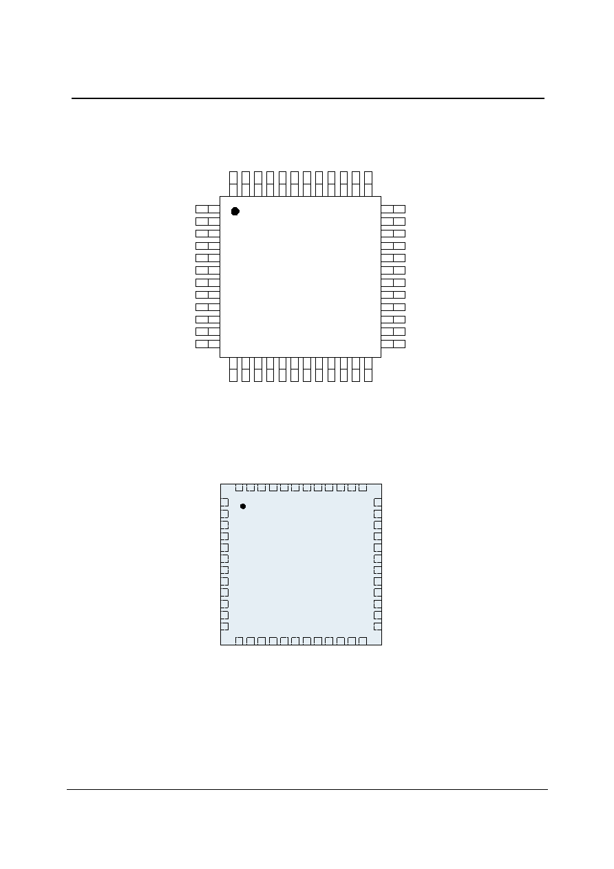
PIN CONFIGURATION
DVDD1
DGND2
BITCLK
SDATAOUT
DGND1
XTLOUT
XTLIN
SDATAIN
DVDD2
SYNC
RESETB
PCBEEP
MO
N
O
O
U
T
A
G
ND2
HP
O
U
T
R
HP
G
N
D
HP
O
U
T
L
A
V
DD2
SP
D
I
F
EA
P
D
/
BU
S
Y
P
E
NDE
T
CI
D
0
MA
S
K
/
L
R
C
CDG
ND
X-/
A
U
X
R
CDL
Y
-
/V
ID
R
Y
+
/V
ID
L
X+
/
A
U
X
L
MI
C
2
LIN
E
IN
R
LI
N
E
I
N
L
MI
C
1
CD
R
LINEOUTR
AUXADC
BMON
CAP2
CX3D1
CX3D2
LINEOUTL
AVDD1
AGND1
VREF
VREFOUT
PDRES
1
9
8
7
6
5
4
3
2
12
11
10
14
21
20
19
18
17
16
15
24
23
22
13
25
31
30
29
28
27
26
36
35
34
33
32
48
38
39
40
41
42
43
44
45
46
47
37
SPE
N
/
I
2
S
PH
O
N
E
Figure 1 TQFP Pinout
47
46
45
48
44
43
42
41
40
39
38
37
14
15
16
13
17
18
19
20
21
22
23
24
1
2
3
4
5
6
7
8
9
10
11
12
36
35
34
33
32
31
30
29
28
27
26
25
LINEOUTR
DVDD1
LINEOUTL
CX3D2
CX3D1
CAP2
BMON
AUXADC
PDRES
VREFOUT
VREF
AGND1
AVDD1
XTLIN
XTLOUT
DGND1
SDATAOUT
BITCLK
DGND2
SDATAIN
DVDD2
SYNC
RESETB
PCBEEP
E
APD
/
BU
S
Y
SP
D
I
F
CI
D0
P
E
NDE
T
HP
O
U
T
L
HP
G
N
D
M
O
N
OOU
T
A
V
DD2
M
ASK
/
L
R
C
S
P
E
N
/ I2S
HP
O
U
T
R
AG
N
D
2
X+
/
AU
XL
PH
O
N
E
Y+
/
VI
D
L
X- /
AU
XR
CD
L
Y-
/
VI
D
R
CDR
CD
G
N
D
MI
C
2
MI
C
1
LIN
E
IN
R
LI
N
E
I
N
L
Figure 2 QFN Pinout

WM9705
Advance Information
AI Rev 3.6 October 2002
4
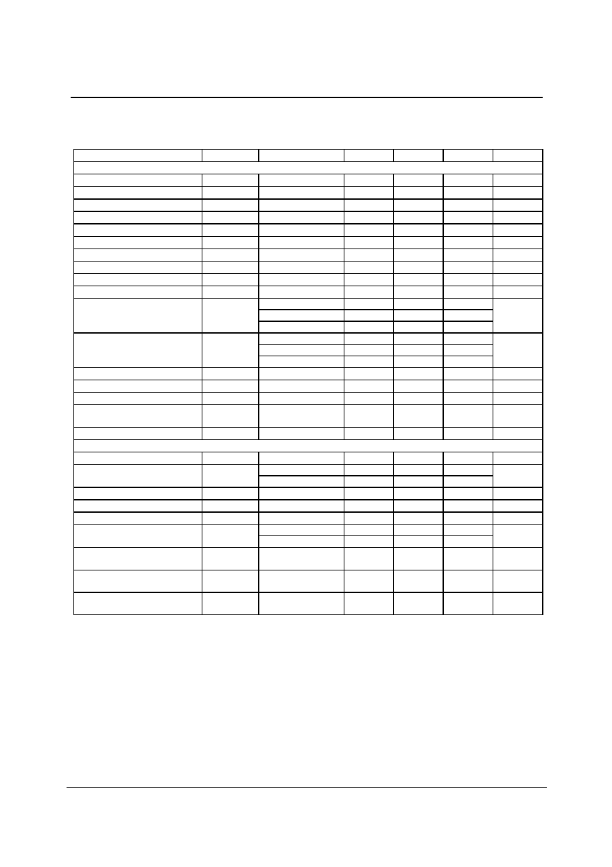
PIN DESCRIPTION
PIN
48 PIN QFN
48 PIN TQFP
TYPE
DESCRIPTION
1
DVDD1
DVDD1
Supply
Digital positive supply
2
XTLIN
XTLIN
Digital input
Clock crystal connection or clock input (XTAL not used)
3
XTLOUT
XTLOUT
Digital output
Clock crystal connection
4
DGND1
DGND1
Supply
Digital ground supply
5
SDATAOUT
SDATAOUT
Digital input
Serial data input
6
BITCLK BITCLK
Digital
output
Digital input
Serial interface clock output to AC'97 controller
or input from AC'97 primary codec
7
DGND2
DGND2
Supply
Digital ground supply
8
SDATAIN
SDATAIN
Digital output
Serial data output to AC'97 controller
9
DVDD2
DVDD2
Supply
Digital positive supply
10
SYNC
SYNC
Digital input
Serial interface sync pulse from AC'97 controller
11
RESETB
RESETB
Digital input
NOT reset input (active low, resets registers)
12
PCBEEP
PCBEEP
Analogue input
Mixer input, typically for PCBEEP signal (also input to AUX ADC)
13
PHONE
PHONE
Analogue input
PHONE input (also input to AUX ADC)
14
X+/AUXL
X+/AUXL
Analogue I/O
Pen X+ channel screen driver/input. (or AUXL mixer input)
15
X-/AUXR
X-/AUXR
Analogue I/O
Pen X- channel screen driver/input (or AUXR mixer input)
16
Y+/VIDL
Y+/VIDL
Analogue I/O
Pen Y+ channel screen driver/input (or VIDL mixer input)
17
Y-/VIDR
Y-/VIDR
Analogue I/O
Pen Y- channel screen driver/input (or VIDR mixer input)
18
CDL
CDL
Analogue input
Mixer input, typically for CD signal
19
CDGND
CDGND
Analogue input
CD input common mode reference (ground)
20
CDR
CDR
Analogue input
Mixer input, typically for CD signal
21
MIC1
MIC1
Analogue input
Mixer input with extra gain if required ≠ also HSET detect input
22
MIC2
MIC2
Analogue input
Mixer input with extra gain if required
23
LINEINL
LINEINL
Analogue input
Mixer input, typically for LINE signal
24
LINEINR
LINEINR
Analogue input
Mixer input, typically for LINE signal
25
AVDD1
AVDD1
Supply
Analogue positive supply for screen drivers
26
AGND1
AGND1
Supply
Analogue ground supply for screen drivers
27
VREF
VREF
Analogue output
Internal reference (buffered CAP2)
28
VREFOUT
VREFOUT
Analogue output
Reference for microphones (buffered CAP2)
29
PDRES
PDRES
Analogue input
Pen Down Detect Pull-up external resistor connection
30
AUXADC
AUXADC
Analogue input
AUX signal input to digitiser ADC
31
BMON
BMON
Analogue input
Battery input to ADC
32
CAP2
CAP2
Analogue I/O
Reference input/output; pulls to midrail if not overdriven
33
CX3D1
CX3D1
Analogue output
Output pin for 3D difference signal
34
CX3D2
CX3D2
Analogue input
Input pin for 3D difference signal
35
LINEOUTL
LINEOUTL
Analogue output
Main analogue output for left channel
36
LINEOUTR
LINEOUTR
Analogue output
Main analogue output for right channel
37
MONOOUT
MONOOUT
Analogue output
Main mono output
38
AVDD2 AVDD2
Supply
Analogue
positive
supply
39
HPOUTL
HPOUTL
Analogue output
Left channel line level output (or headphone, or headset mic input)
40
HPGND
HPGND
Supply
Headphone ground supply
41
HPOUTR
HPOUTR
Analogue output
Right channel line level output (or headphone)
42
AGND2
AGND2
Supply
Analogue ground supply
43
MASK/LRC
MASK/LRC
Digital bidir
MASK input signal to delay PEN conversions (or LRCLK output)
44
SPEN/I
2
S SPEN/I
2
S
Digital bidir
SPDIF hardware enable pin and I
2
S data output
45
CID0
CID0
Digital input
Primary/Secondary ID select (internal pull-up) Hi = Primary
46
PENDET
PENDET
Digital output
Pen Down Detection flag OR Headset detect output
47
EAPD/BUSY
EAPD/BUSY
Digital output
External amplifier powerdown or BUSY output flag from Pen ADC
48
SPDIF
SPDIF
Digital output
S/PDIF output

WM9705
Advance Information
AI Rev 3.6 October 2002
5
ELECTRICAL CHARACTERISTICS
Test Characteristics:
AVDD = 3.3V, DVDD = 3.3V, 48kHz audio sampling, T
A
= 25
o
C, unless otherwise stated.
PARAMETER SYMBOL
TEST
CONDITIONS
MIN
TYP
MAX
UNIT
Digital Logic Levels (DVDD = 3.3V)
Input LOW level
V
IL
DGND - 0.3
0.8
V
Input HIGH level
V
IH
2.2
DVDD
+
0.3
V
Output LOW
V
OL
I Load = 2mA
0.10 x DVDD
V
Output HIGH
V
OH
I Load = -2mA
0.90 x DVDD
V
Analogue Audio I/O Levels (Input Signals on any audio inputs, Outputs on LINEOUT L, R and MONO and HPOUT L,R)
Input level
Minimum input
impedance = 10k
AGND
-100mV
AVDD
+100mV
V
Output level to LINEOUT L,R
Into 10kohm load
AGND
+300mV
ear rail to rail
AVDD
-300mV
V
Output level to HPOUT L,
HPOUTR and MONOOUT
Into 16 ohm load
AGND
+300mV
ear rail to rail
AVDD
-300mV
V
Reference Levels
Reference input/output
CAP2
0.47 AVDD
0.50 AVDD
0.53 ACDD
V
CAP2 impedance
75
k
Mixer reference
VREF
Buffered
CAP2
V
MIC reference
VREFOUT
Buffered
CAP2
V
MIDBUFF current source
(pins VREF and VREFOUT)
AVDD = 3.3V
5
10
mA
MIDBUFF current sink
(pins VREF and VREFOUT)
AVDD = 3.3V
-5
-10
mA
AUDIO DAC to Line-out (10k
:
load)
SNR A-weighted (Note 1)
85
91
dB
Full scale output voltage
VREF
= 1.65V
0.7
Vrms
Total Harmonic Distortion + Noise
THD+N
-3dB FS input
-84
0.006
-74
0.02
dB
%
PSRR
20 to 20kHz, without
supply decoupling
-40 dB
AUDIO ADC
ADC input for full scale output
VREF
= 1.65V
0.7
Vrms
Signal to Noise Ratio
A-weighted (Note 1)
SNR 80
86
dBFS
Total Harmonic Distortion+Noise
THD+N -6dBFS
input
-79
-72 dB
Power Supply Rejection Ratio
PSRR
20 to 20kHz, without
supply decoupling
-40
dB
Digital Filter Characteristics
Frequency response
20
19,200 Hz
Transition band
19,200
28,800 Hz
Stop band
28,800
Hz
ADC -74
Stop band attenuation
DAC -40
dB

WM9705
Advance Information
AI Rev 3.6 October 2002
6
Test Characteristics:
AVDD = 3.3V, DVDD = 3.3V, 48kHz audio sampling, T
A
= 25
o
C, unless otherwise stated.
PARAMETER SYMBOL
TEST
CONDITIONS
MIN
TYP
MAX
UNIT
Mixer Inputs to Line-out (10k
:
load)
Maximum input voltage
AGND
0.7
AVDD Vrms
Maximum output voltage
on
LINEOUT
0.7
Vrms
CD inputs
90
97
Signal to Noise Ratio
A-weighted (Note 1)
SNR
Other inputs
82
95
dB
CD and LINE inputs
-87
0.0044
-77
0.014
PHONE input
-82
0.008
-71
0.028
MIC1 input
-82
0.008
-71
0.028
MIC2 input
-90
0.003
-71
0.028
Total Harmonic Distortion + Noise
-1dBFS input
THD+N
PCBEEP input
-78
0.013
-67
0.045
dB
%
Input impedance (CD inputs)
At any gain
15
kohm
At max gain
10
20
kohm
Input impedance (other mixer
inputs)
At 0db gain
50
100
kohm
At max gain
10
30
kohm
Input impedance MIC inputs
At 0db gain
55
110
kohm
Power Supply Rejection Ratio
PSRR
20 to 20kHz, without
supply decoupling
-40
dB
Headphone Buffer (pins HPOUTL, HPOUR and MONOOUT)
Maximum output voltage
0.7
Vrms
RL = 32 Ohms
30
mW
Max Output Power (Note 1)
P
O
RL = 16 Ohms
40
mW
SNR (Note 2)
A-weighted 85 92
dB
1kHz, R
L
= 32 ohms @
P
O
= 10mW rms
-80
0.01
-60
0.1
dB
%
Total Harmonic Distortion + Noise
THD+N
1kHz, R
L
= 32 ohms @
P
O
= 20mW rms
-77
0.014
-40
1.0
dB
%
Power Supply Rejection Ratio
PSRR
20 to 20kHz, without
supply decoupling
-40
dB
Clocks
Crystal clock
24.576
MHz
BITCLK frequency
12.288
MHz
SYNC frequency
48.0
KHz
WM9705
Advance Information
w
AI Rev 3.6 October 2002
7
Test Characteristics:
AVDD = 3.3V, DVDD = 3.3V, MCLK= 24.576MHz, T
A
= 25
o
C, unless otherwise stated.
PARAMETER
SYMBOL
TEST CONDITIONS
MIN
TYP
MAX
UNIT
PEN andAUXILIARY INPUT ADC
Resolution
12
Bits
Differential non-linearity error
DNL
+/-0.25
LSB
Integral non-linearity error
INL
+/-2
LSB
Offset error
+/-4
LSB
Gain error
+/-4
LSB
Noise
500
µ
Vrms
Conversion time
20.8
µ
sec
Acquisition time
15
µ
sec
Throughput rate
48
kHz
Multiplexer settling time
500
nsec
X conversion
X+ pin
Y conversion
Y+ pin
ADC positive reference
auxiliary conversion
AVDD1
V
X conversion
X- pin
Y conversion
Y- pin
ADC negative reference
auxiliary conversion
AGND1
V
AUXADC input range (fullscale)
AGND1
AVDD1
BMON input range
AGND1
6.5V
BMON input impedance
at sampling time
30
k
BMON effective input
impedance (Note 3)
93.75Hz sample rate
7.7
M
BMON input gain
1/3
PEN INTERFACE
Full scale input range
AVDD
V
Positive input
AVDD
Absolute input range
Negative input
0
V
Capacitance
5
pF
Leakage current
0.5
µ
A
Screen switch on resistance
20
PIL = 0
200
Pressure measurement current
PIL = 1
400
µ
A
External Pen-detect pull up
resistor value
1
10
100
k
Pen Detect Comparator
Threshold DAC Range
PDDACR
0.1
1.65
V
Pen Detect Comparator
Threshold DAC step size
PDDACLSB
0.1
V
Note:
1.
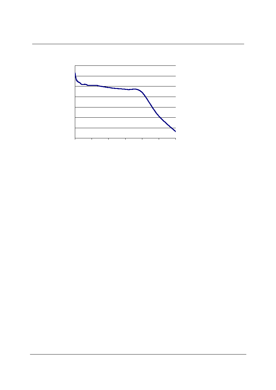
Harmonic distortion on the headphone output decreases with output power ≠ see Figure 3.
2.
SNR is the ratio of 0dB signal amplitude to noise floor with no signal present (all 0s input code to DACs).
3.
The input impedance of the BMON input is 30k to ground when the ADC is sampling and hi-Z when it is not. The effective
input resistance is calculated dependant on how often the battery is sampled by the user. 7.7M Ohms is the effective
impedance if the battery is sampled once every 512 frames. For a fuller description of this and information on how to
calculate the effect input impedance please see the section on auxiliary conversions on pages 46.
WM9705
Advance Information
AI Rev 3.6 October 2002
8
-100
-90
-80
-70
-60
-50
-40
-30
0
5
10
15
20
25
30
Output Power (mW)
T
H
D+
No
i
s
e
(
d
B
)
Figure 3 Distortion Versus Power on Headphone Outputs, using 32 Ohm Load and AVDD = HPVDD = 3.3V

WM9705
Advance Information
AI Rev 3.6 October 2002
9
POWER CONSUMPTION
Test Characteristics:
AVDD = 3.3V, DVDD = 3.3V, AGND = 0V ..............T
A
= 25
o
C, unless otherwise stated.
CURRENT CONSUMPTION
MODE
DESCRIPTION
PR
0
PR
1
PR
2
PR
3
PR
4
PR
5
PR
6
EA
P
D
D
I
G
I
T
I
SE
R
PD
RE
G
7
8
H
(
P
RP
)
RE
CO
R
D
M
U
X
MIN TYP
MAX
UNITS
Record and Playback
Mic Record (note 1)
0 0 0 0 0 0 0 X 00
000L
000R
14.8 (A)
14.3 (D)
mA
Other Input Record
0 0 0 0 0 0 0 X 00
001L
001R
17.7 (A)
14.3 (D)
mA
Other Input Record
PR6
0 0 0 0 0 0 1 X 00
001L
001R
16.3 (A)
14.3 (D)
mA
Other Input Record
PR6 and PR2
0 0 1 0 0 0 1 X 00
001L
001R
10.7 (A)
14.3 (D)
mA
Other Input Record
PR6 and PR3
0 0 0 1 0 0 1 X 00
001L
001R
0.5 (A)
14.1 (D)
mA
Playback Only
Low Power Playback
(note 2)
1 0 1 0 0 0 0 X 00
001L
001R
5.5 (A)
11.5 (D)
mA
Playback Only
1 0 0 0 0 0 0 X 00
001L
001R
11.1 (A)
11.5 (D)
mA
Playback Only
PR6
1 0 0 0 0 0 1 X 00
001L
001R
9.7 (A)
11.5 (D)
mA
Playback Only
PR6 and PR2
1 0 1 0 0 0 1 X 00
001L
001R
4.0 (A)
11.5 (D)
mA
Playback Only
PR6 and PR3
1 0 0 1 0 0 1 X 00
001L
001R
0.4 (A)
11.5 (D)
mA
Record Only
Mic Record (note 1) 0 1 0 0 0 0 0 X 00
000L
000R
12.9 (A)
13.3 (D)
mA
Other Input Record
0 1 0 0 0 0 0 X 00
100L
100R
15.8 (A)
13.3 (D)
mA
Other Input Record
PR6
0 1 0 0 0 0 1 X 00
100L
100R
14.3 (A)
11.3 (D)
mA
Other Input Record
PR6 and PR2
0 1 1 0 0 0 1 X 00
100L
100R
7.2 (A)
13.3 (D)
mA
Other Input Record
PR6 and PR3
0 1 0 1 0 0 1 X 00
100L
100R
0.3 (A)
12.9 (D)
mA
Power Down
Power Down
(note 3)
1 1 1 1 1 1 1 X 00
XXXL
XXXR
0.1 (A)
2.0 (D)
uA
Pen Digitiser
Pen Digitiser
(Note 4)
1 1
1 1 0 1 1 X 11
XXXL
XXXR
0.1 (A)
3.6 (D)
mA
Notes:
1.
When the ADC input mux is set to mic input to BOTH ADC channels, (SR2-0 and SL2-0 both set to `0'), one ADC is shared
between both channels and the other is powered off to save current. The same digital data is output to both slots.
2.
The POP bit (reg 20h) also needs to be set for this mode.
3.
These values are recorded with no external clocks applied to the WM9705.
4.
Pen active duty cycle is approximately 10%. Average analogue current consumption is approximately 10% of stated figure.
WM9705
Advance Information
AI Rev 3.6 October 2002
10
DETAILED TIMING DIAGRAMS
Test Characteristics:
AVDD = 3.3V, DVDD = 3.3V, AGND = 0V ..............T
A
= 0
o
C to +70
o
C, unless otherwise stated.
All measurements are taken at 10% to 90% DVDD, unless otherwise stated. All the following timing information is guaranteed, not
tested.
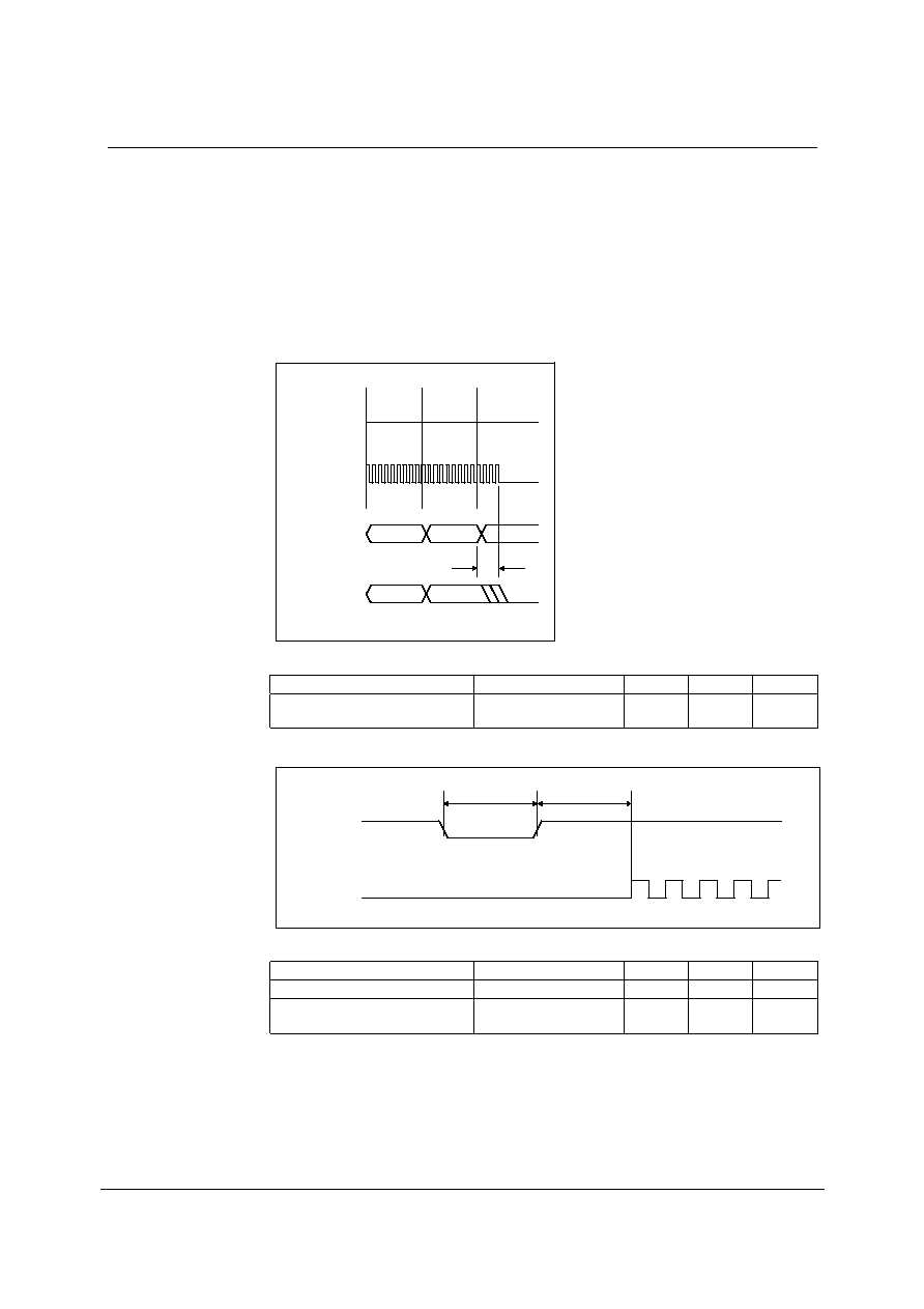
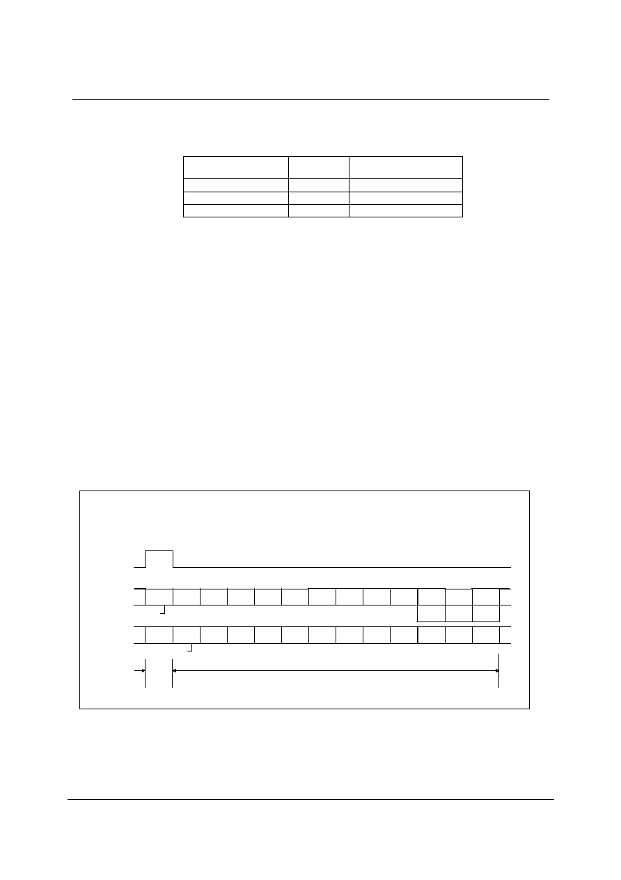
AC-LINK LOW POWER MODE
SYNC
BITCLK
SDATAOUT
WRITE
TO 0X20
DATA PR4
DON'T
CARE
SDATAIN
SLOT 1
SLOT 2
t
S2_PDOWN
Figure 4 AC-Link Powerdown Timing
PARAMETER SYMBOL
MIN
TYP
MAX
UNIT
End of slot 2 to BITCLK SDATAIN
low
t
S2_PDOWN
1.0
µ
s
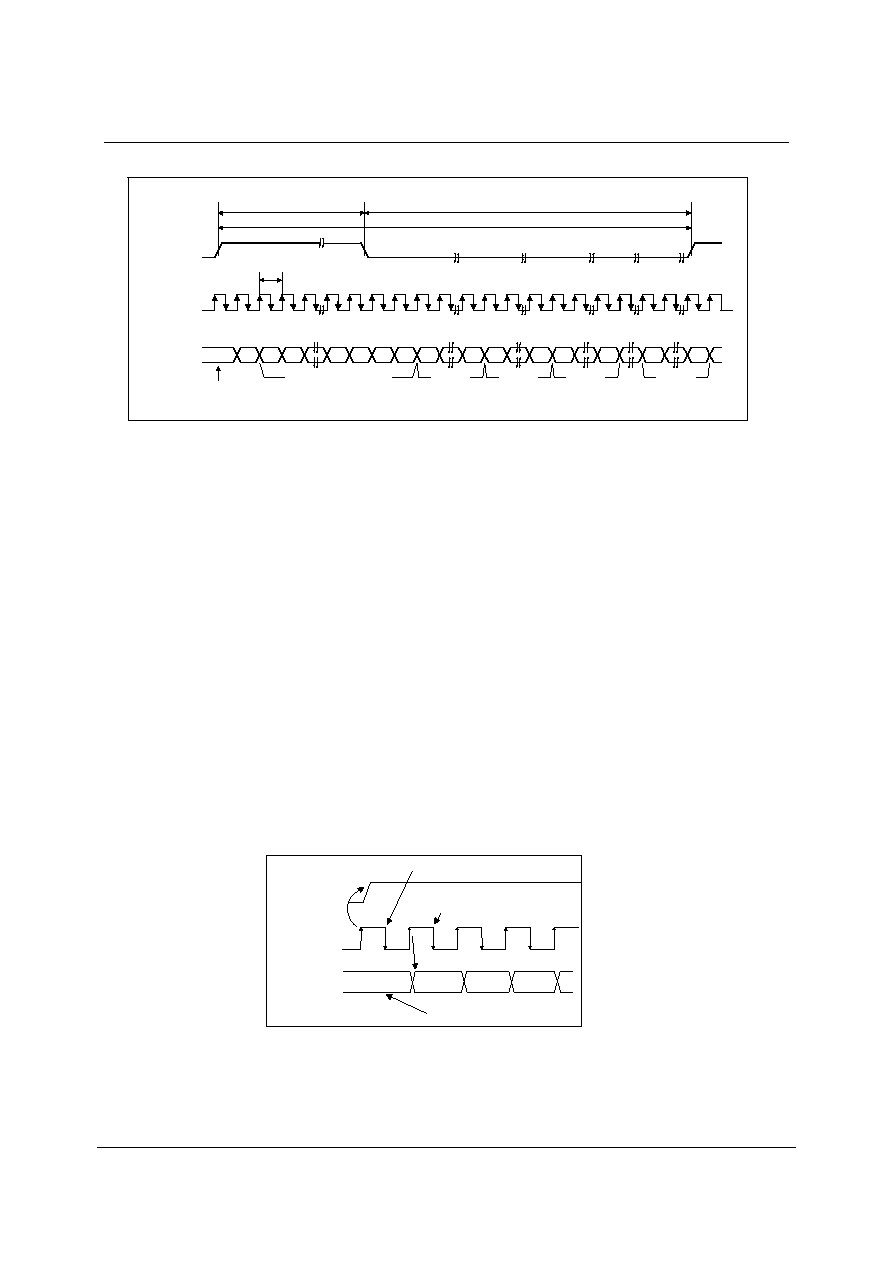
COLD RESET
RESETB
BITCLK
t
RST_LOW
t
RST2CLK
Figure 5 Cold Reset Timing
PARAMETER SYMBOL
MIN
TYP
MAX
UNIT
RESETB active low pulse width
t
RST_LOW
1.0
µ
s
RESETB inactive to BITCLK
startup delay
t
RST2CLK
162.8
ns

WM9705
Advance Information
AI Rev 3.6 October 2002
11
WARM RESET
SYNC
BITCLK
t
SYNC_HIGH
t
SYNC2CLK
Figure 6 Warm Reset Timing
PARAMETER SYMBOL
MIN
TYP
MAX
UNIT
SYNC active high pulse width
t
SYNC_HIGH
1.3
µ
s
SYNC inactive to BITCLK startup
delay
t
SYNC2CLK
162.4
ns
CLOCK SPECIFICATIONS
BITCLK
SYNC
t
CLK_HIGH
t
CLK_LOW
t
CLK_PERIOD
t
SYNC_HIGH
t
SYNC_LOW
t
SYNC_PERIOD
Figure 7 Clock Specifications (50pF External Load)
PARAMETER SYMBOL
MIN
TYP
MAX
UNIT
BITCLK frequency
12.288
MHz
BITCLK period
t
CLK_PERIOD
81.4 ns
BITCLK output jitter
750
ps
BITCLK high pulse width (Note 1)
t
CLK_HIGH
36 40.7 45 ns
BITCLK low pulse width (Note 1)
t
CLK_LOW
36 40.7 45 ns
SYNC frequency
48.0 kHz
SYNC period
t
SYNC_PERIOD
20.8
µ
s
SYNC high pulse width
t
SYNC_HIGH
1.3
µ
s
SYNC low pulse width
t
SYNC_LOW
19.5
µ
s
Note:
Worst case duty cycle restricted to 45/55.

WM9705
Advance Information
AI Rev 3.6 October 2002
12
DATA SETUP AND HOLD (50PF EXTERNAL LOAD)
BITCLK
SDATAOUT
SDATAIN
SYNC
t
SETUP
t
HOLD
t
SETUP
t
HOLD
Figure 8 Data Setup and Hold (50pF External Load)
Note:
Setup and hold time parameters for SDATAIN are with respect to AC'97 Controller.
PARAMETER SYMBOL
MIN
TYP
MAX
UNIT
Setup to falling edge of BITCLK
t
SETUP
10 ns
Hold from falling edge of BITCLK
t
HOLD
10 ns
SIGNAL RISE AND FALL TIMES
BITCLK
SYNC
SDATAIN
SDATAOUT
trise
CLK
tfall
CLK
trise
SYNC
tfall
SYNC
trise
DIN
tfall
DIN
trise
DOUT
tfall
DOUT
Figure 9 Signal Rise and Fall Times (50pF External Load)
PARAMETER SYMBOL
MIN
TYP
MAX
UNIT
BITCLK rise time
trise
CLK
2 6
ns
BITCLK fall time
tfall
CLK
2 6
ns
SYNC rise time
trise
SYNC
2 6
ns
SYNC fall time
tfall
SYNC
2 6
ns
SDATAIN rise time
trise
DIN
2 6
ns
SDATAIN fall time
tfall
DIN
2 6
ns
SDATAOUT rise time
trise
DOUT
2 6
ns
SDATAOUT fall time
tfall
DOUT
2 6
ns

WM9705
Advance Information
AI Rev 3.6 October 2002
13
DEVICE DESCRIPTION
INTRODUCTION
This specification describes the WM9705 audio codec, which is designed to be software and
hardware compatible with the Intel AC'97 rev2.2 component specification. The device is a derivative of
the basic AC'97 codec, with added support for resistive touch-screen pen inputs. Variable Rate Audio
(VRA) is supported at rates defined in the Intel rev2.1 or rev2.2 specification, and a SPDIF output port
is provided which may optionally be used to output the PCM DAC information to external processors.
A key feature of operation of the pen digitiser function is the cessation of screen drive activity when the
pen is lifted from the screen, so minimising audio performance degradation and reducing power
consumption.
WM9705 offers the following features:
Stereo Audio Codec with Intel specified VRA support of different audio sample rates
Pen Digitiser function with 4-wire pen interface and support for pen-down detection, pen pressure
measurement and wake-on-pen-down.
Auxiliary ADC inputs for temperature, supply and battery monitoring.
Pen-down flag and ADC BUSY flags, output to pins, and MASK input pin provided to allow delay of
pen conversions in event of LCD activity
Optional SPDIF and I
2
S audio outputs (SPDIF output may be hardware enabled so needing no driver
support)
Headphone drive capability and optional auto detection of headset or headphone plug in
It is highly recommended that the Intel AC'97 rev2.2 specification be studied in parallel with this
document: This specification can be downloaded from the Intel web site.
The WM9705 is fully operable on 3V or 5V or mixed 3/5V supplies, and is packaged in the industry
standard 48pin TQFP package with 7mm body size.
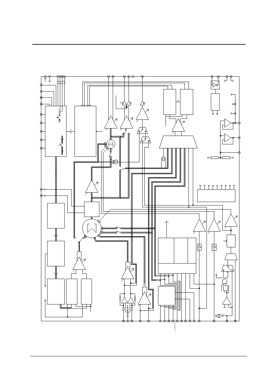
Figure 10 shows the functional block diagram including control register bit locations for WM9705.
AC'97 FEATURES
WM9705 implements the base set of AC'97 rev2.2 features, plus several enhancements:
All rev2.2 specified variable audio sample rates supported
3-D stereo enhancement feature.
Headphone support on AUX outputs (pins 39,41)
Primary/secondary codec operation by pin programming of CID0 pin
SPDIF audio output with rev2.2 compliant control set.

WM9705
Advance Information
AI Rev 3.6 October 2002
14
NON - AC'97 FEATURES
In addition to the AC'97 features offered, WM9705 also supports:
4-wire pen digitiser with integrated screen driver, featuring highly flexible modes of operation,
supporting autonomous screen conversions, and auxiliary conversions. Screen X and Y connections
driven from AUX and VID stereo input pins, which are still connected.
Headphone drive capability on MONO output, with extra signal routing switch PSEL, allowing PHONE
input to be routed to MONO output
Extra switch HPND after the mixer allowing MIX without DAC signal to be output to headphone
outputs, and so allowing DAC with no MIX to be output to LINE outputs.
I
2
S audio output capability, in addition to SPDIF output, allowing support of an extra external audio
DAC for multi-channel solutions. SPDIF output may be hardware enabled.
Option to route the stereo audio ADC output to the SPDIF and/or I
2
S digital outputs
Auto-detect of headphones or headset plugged into the AUX headphone outputs, with internal routing
of microphone signal from the headphone pin to the MIC1 input.
Battery monitoring input BMON that supports direct connection to battery voltages up to 6.5V.
MPM switch allowing mix of DAC + mixer output onto MONOUT and independent mix of DAC +
PHONE and/or PCBEEP onto LINEOUT or HPOUT.
Reset powerdown override ≠ holding MASK high in reset overrides the PR bits forcing the WM9705
into a low power mode
W
M
9
705
A
d
v
a
nce
Info
r
m
a
t
i
o
n
A
I
R
e
v
3
.
6 O
c
t
o
b
e
r
20
02
15
RECORD
ADCCLK
SYNCH
BITCLK
DVDD1&2
DACCLK
and Filter
DACR
Multibit DAC
and Filter
DACL
Multibit DAC
Mux
Mono
ADCCLK
WM '3-D'
MIXREF
DACREF
ADCREF
PGA
Reg 72h
ENHANCE
Reg 22h
MUX
Reg 1Ah
Serial Interface
PGA
Reg 18h
PGA
Reg 1Ch
ADC PGA
CAP2 (32) VREFOUT (28) VREF (27)
AVDD2 (38)
MONOOUT (37)
LINEOUTR (36)
LINEOUTL (35)
(4)
(7)
(1)
(9)
(11)
(5)
(8)
(10)
(6)
(33)
(34)
PCBEEP(12)
MIC1 (21)
MIC2 (22)
AUDIO DAC PGA
AUDIO DACs
AUDIO MIXER PGA
Modulator
Analogue
Sigma Delta
ADCREF
ADC Decimation filters
Analogue
Sigma Delta
Modulator
CLOCK
GENERATOR
ADCCLK
DACCLK
XTLOUT (3)
XTLIN (2)
POWER
ENABLE
reg 26h
EAPD
(Prim/Sec)
&
(29)
(30)
(31)
PEN INPUT and
PGA
Reg 04h
(typ)
HEADPHONE
BUFFERS
HP VOLUME
PDRES
Pen inputs
EAPD/BUSY
(47)
PENDET (46)
POP (20h)
LEFT AUDIO
RIGHT AUDIO
HPGND (40)
DACREF
2 x 18 bit
Variable
Rate Audio
Support
DAC
Interpolation
Filters
Modulators
Sigma Delta
Digital
with pen input
(5Ch)
ADC PCM
DATA
DAC
ADC
LPBK
(reg 20h)
DAC PCM Data
WM9705
reg 78h
PRP
AUXILIARY ADC
PEN Digitiser
AVDD1 (25)
PHONE (13)
screen supplies
screen switches
MASK/LRC (43)
SPEN/I2S (44)
SPDIF (48)
PGA
PGA
Reg 12h
Reg 10h
CDL (18)
CDGND (19)
CDR (20)
X+/AUXL (14)
Y+/VIDL (16)
Y-/VIDR (17)
X-/AUXR (15)
R
e
g
14h
b15
R
e
g
16h
b15
PGA
Reg 02h
(typ)
AUDIO VOLUME
PGA
Reg 06h
MIX (20h)
PSEL(5Ch)
MONO VOLUME
BUFFER
HEADPHONE
MHPZ (5Ch)
PR6
R
L
HPND
(5Ch)
+20dB
Mux
Mic
PGA
Reg 0Eh
20dB (0Eh)
MS (20h)
COMP
HS
HSEN
0
1
0
1
PR0 ADC EN
PR1
PR2
PR3
PR4
PR5
DAC EN
MIX EN
REF EN
LNK EN
CLK EN
PR6 HP EN
AUXADC
BMON
PR6 OR HSDT
MPUE
5mA
VMID
HSDT
HSCP
1
0
1
0
1
0
To output slot
of AC link
7Ah
or register
PEN Function Control
registers 76h & 78h
Mux
Input
State Control machine
PGA
Reg 0Ch
PGA
Reg 0Ah
PHIZ
PHIZ
R
L
ADCNDAC
AC97 rev2.2 Codec
CX3D2
CX3D1
DGND1&2
CID (45)
HPOUTL (39)
HPOUTR (41)
AGND2 (42)
HPOUTL
AGND1 (26)
LINEINL (23)
LINEINR (24)
(5Ch)
SPEN, ADCO & I2S
SDATAOUT
RESETB
SDATAIN
MPM
(5Ah)
HPB (74h)
Fi
gu
re
1
0
F
u
n
c
t
i
on
a
l
B
l
oc
k
D
i
a
g
r
a
m

WM9705
Advance Information
AI Rev 3.6 October 2002
16
PEN DIGITIZER AND AUXILIARY ADC
A 4 wire input pen digitiser function is included on WM9705. This circuit comprises driver circuits to
drive typical resistive touch screens of the type used on PDA's, plus a 12 bit resolution ADC to convert
pen input values. This ADC may also be used to perform additional auxiliary ADC conversions of the
levels present on the AUXADC, BMON, PCBEEP or PHONE pins. A control bit (PHIZ in register 78h)
is provided to allow PCBEEP and PHONE inputs to be made high impedance (internally disconnected
so signal paths are cut) if required.
Operation of the pen digitiser function is controlled from digitiser control registers 76h and 78h. The
ADC conversion result is obtained by reading from the contents of bits [11-0] in register 7Ah, or
optionally by enabling the AC link SLOT transfer method, when results are sent back in the AC'97 slot
data format. The pen digitiser ADC is a 12bit successive approximation type converter with excellent
differential non-linearity performance.
The pen digitiser ADC may be used to convert either pen input data, or the voltages present on the
AUXADC, BMON, PCBEEP or PHONE pins. Such functions as battery monitoring or temperature
measurement might therefore be implemented.
The following pen digitiser features are available:
Support for wake-on-pen-down
Pen down detection, pressure measurement, auxiliary conversions
MASK conversion delay override or synchronous operation option
SLOT or R/W register data transfer
Programmable screen drive to sample taken delay
Programmable Pen-down detection threshold
Details of pen digitiser operation are available in the Pen Digitiser description section. Note that the
pins allocated for X/Y screen connections are those that would normally be used for AUX and VID
stereo inputs in a conventional AC '97 codec. In WM9705 these pins remain connected to the MIXER
and ADC inputs, and may be used as analogue inputs, with the restriction that gain through the mixer
input is fixed at 0dB. The normal MUTE function is provided using bit 15 in the appropriate register. It
is recommended that these MUTE bits are left `mute' whenever the screen is driven. Reading back the
registers will report 0dB gain, and the MUTE value as programmed. ADC gain control on the AUX and
VID inputs works as normal.
3-D STEREO ENHANCEMENT
This device contains a stereo enhancement circuit, designed to optimise the listening experience when
the device is used in a typical PC operating environment. That is, with a pair of speakers placed either
side of the monitor with little spatial separation. This circuit creates a difference signal by differencing
left and right channel playback data, then filters this difference signal using lowpass and highpass
filters whose time constants are set using external capacitors connected to the CX3D pins 33 and 34.
Typically the values of 100nF and 47nF set highpass and lowpass poles at about 100Hz and 1kHz
respectively. This frequency band corresponds to the range over which the ear is most sensitive to
directional effects.
The filtered difference signal is gain adjusted by an amount set using the 4-bit value written to Register
22h bits 3 to 0. Value 0h is disable, value Fh is maximum effect. Typically a value of 8h is optimum.
The user interface would most typically use a slider type of control to allow the user to adjust the level
of enhancement to suit the program material. Bit D13 3D in Register 20h is the overall 3D enable bit.
The Reset Register 00h reads back the value 11000 in bits D14 to D10. This corresponds to decimal
24, which is registered with Intel as Wolfson Stereo Enhancement.
Note that the external capacitors setting the filtering poles applied to the difference signal may be
adjusted in value, or even replaced with a direct connection between the pins. If such adjustments are
made, then the amount of difference signal fed back into the main signal paths may be significant, and
can cause large signals which may limit, distort, or overdrive signal paths or speakers. Adjust these
values with care, to select the preferred acoustic effect. There is no provision for pseudo-stereo
effects. Mono signals will have no enhancement applied (if the signals are in phase and of the same
amplitude). Signals from the PCM DAC channels can have stereo enhancement applied. It can also
be bypassed if desired. This function is enabled by setting the bit POP in Register 20h.

WM9705
Advance Information
AI Rev 3.6 October 2002
17
VARIABLE SAMPLE RATE SUPPORT
The DACs and ADCs on this device support all the recommended sample rates specified in the Intel
AC'97 rev2.1 & rev2.2 specifications for audio rates. The default rate is 48ks/s. If alternative rates are
selected and variable rate audio is enabled (Register 2Ah, bit 0), the AC'97 interface continues to run
at 48k words per second, but data is transferred across the link in bursts such that the net sample rate
selected is achieved. It is up to the AC'97 Revision 2.1/2 compliant controller to ensure that data is
supplied to the AC link, and received from the AC link, at the appropriate rate.
Variable rates are selected by writing to registers 2Ch (DAC) and 32h (ADC). ADC and DAC rates
may be set independently, with left and right channels always at the same rate. Note that register 2Ch
should only be written to when the DAC is powered ON, similarly register 32h should only be written to
when the ADC is powered ON (see register 26h for power control). The device supports on demand
sampling. That is, when the DAC signal processing circuits need another sample, a sample request is
sent to the controller which must respond with a data sample in the next frame it sends. For example,
if a rate of 24ks/s is selected, on average the device will request a sample from the controller every
other frame, for each of the stereo DACs. Note that if an unsupported rate is written to one of the rate
registers, the rate will default to the nearest rate supported. The Register will then respond, when
interrogated, with the supported rate the device has defaulted to.
The WM9705 clocks will scale automatically dependent upon the MCLK frequency, where MCLK is
not equal to 24.576MHz. With a 24MHz clock the BCLK frequency expected will be 12MHz and the
sampling frequency (SYNC0 expected is BCLK/256 = 46.875kHz.
AUDIO
SAMPLE RATE
CONTROL VALUE
D15-D0
8000 1F40
11025 2B11
16000 3E80
22050 5622
32000 7D000
44100 AC44
48000 BB80
Table 1 Variable Sample Rates Supported
SPDIF OR I
2
S DIGITAL AUDIO DATA OUTPUT
The WM9705 SPDIF output may be enabled in hardware by holding pin 44 (SPEN) high when
RESETB is taken high, or by writing to the SPDIF control bit in register 2Ah. If SPDIF pin 48 is pulled
high at start-up by a weak pull-up (e.g. 100k), then SPDIF capability bit in register 28h is set to `0', i.e.
no SPDIF capability. This allows for stuffing options, so that when SPDIF external components are not
provided, the driver will see `no SPDIF capability' and `grey out' the relevant boxes in the control panel.
Additionally the digital audio may be output in I
2
S format using pin 44 (SPEN) as the data output, and
outputting a frame clock or LRCLK onto pin 43. The data is clocked onto pin 44 using the regular
BITCLK at 256fs, which would also then be used as the MCLK if the data is taken to an external DAC.
Operation in this mode is selected by setting bit I
2
S in register 5Ch. A 64fs bitclk is also available and
can be output on SPDIF by setting bit I2S64 in register 74h. Note that I
2
S operation is only supported
for 48ks/s operation. Hardware selection of SPDIF operation by pulling pin SPEN `hi' is compatible
with I
2
S operation, provided a weak pull-up (circa 100k) was used to hold SPEN high at start-up. The
SPEN pin becomes I
2
S data output pin when I
2
S is enabled, and the weak pull-up on this pin is
overdriven.
For both SPDIF and I
2
S modes the data that is output may be sent from the WM9705 via the AC link
in the same slots as normal DAC data or may be sent in different slots. The output slots that contain
the SPDIF/I
2
S data are selected by bits SPSA[1:0] in register 2Ah. WM9705 is compliant with AC'97
rev2.2 specification with regard to slot mapping; therefore the default mode of operation is to output
SPDIF or I
2
S data from the next data slots available after the audio data slots currently in use.
Alternatively if required, data may be mapped from any of the available slots by selection using SPSA
bits. The following table shows the default slot mapping for audio DACs and SPDIF/I
2
S data: (further
details in the register description section later).

WM9705
Advance Information
AI Rev 3.6 October 2002
18
SPEN STATE AT
START-UP
CODEC ID (PIN 45 STRAPPING)
AUDIO DAC SLOT DEFAULT
SPDIF OR I
2
S
DATASLOT DEFAULT
`lo' (rev2.2 compliant)
`hi' = ID = 0 = primary
Slots 3 & 4 - front channels
Slots 7 & 8
`lo' (rev2.2 compliant)
`lo' = ID = 1 = secondary
Slots 7 & 8 ≠ surround
Slots 6 & 9
`hi' (WM proprietary)
`hi' = ID = 0 = primary
Slots 3 & 4 - front channels
Slots 3 & 4
`hi' (WM proprietary)
`lo' = ID = 1 = secondary
Slots 7 & 8 ≠ surround
Slots 3 & 4
Table 2 DAC and SPDIF Slot Mapping Defaults
However, an exception to the rev2.2 mapping table is made when SPDIF operation is enabled using
the SPEN hardware enable pin (being held high at start-up): in this case SPDIF data is immediately
output from the DAC primary slots 3 & 4. This allows for driver-less SPDIF operation, where the
SPDIF or I
2
S output is simply the data contained in the main audio DAC channels. Channel status and
control bits output along with the SPDIF data are as set in the SPDIF control register 3Ah. If required
SPDIF data channel slot mapping may be then changed by setting SPSA bits as required. See tables
18, 19 and 20 for further details.
A mode is provided where the output from the ADC is sent out as the SPDIF or I
2
S data as above,
rather than the data sent to the DACs over the AC link. This mode is enabled by setting bit ADCO in
register 5Ch. ADC data continues to be sent via the AC link to the controller as normal.
WM9705 supports SPDIF and I
2
S data only at the default 48ks/s frame rate. Writing to SPSR bits in
register 3Ah any value other than the default 48ks/s rate will result in a fail to write, with the 48ks/s
value being returned on subsequent reads of these values.
PRIMARY/SECONDARY ID SUPPORT
WM9705 supports operation as either a primary or a secondary codec. Configuration of the device as
either a primary or as a secondary, is selected by tying the CID0 pin 45 on the package.
Fundamentally, a device identified as a primary (ID = 0, CID0 = `hi') produces BITCLK as an output,
whereas a secondary (any other ID) must be provided with BITCLK as an input. This has the obvious
implication that if the primary device on an AC link is disabled, the secondary devices cannot function.
The AC'97 Revision 2.2 specification defines that the CID0 pin has inverting sense, and are provided
with internal weak pull ups. Therefore, if no connections are made to the CID0 pin, then the pin pull hi
and an ID = 0 is selected, i.e. primary. External connect to ground (with pull-down from 0 to 10kohm)
will select codec ID = `1'.
PIN 45 CID0
ID SELECTED
PRIMARY OR
SECONDARY
BITCLK
NC or pull-up
0
Primary
Output
Ground 1 Secondary
Input
Table 3 Codec ID Selection
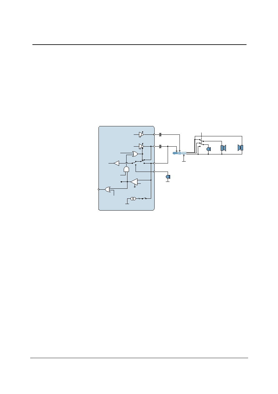
HEADPHONE DRIVE AND HEADSET AUTODETECT
Headphone drive capability is provided on the HPOUT output pins 39 and 41 (called AUXOUT in
AC'97 rev2.2 specification) and also on the MONOOUT output pin 37.
Headphones of impedance typically from 16 ohms upwards may be connected to these pins. AC
coupling with an appropriately sized capacitor is recommended for removal of the mid-rail DC pedestal
present on these outputs. AC'97 rev2.2 specification recommends 32ohm headphones; if a
headphone is connected for use as a headset, where the stereo ear-pieces are driven in parallel, then
each capsule must be of minimum 32ohm impedance.
In many applications it is desirable to be able to connect either a stereo headphone to the headphone
output pins, or a mono headset, comprising ear-piece(s) and a microphone. The microphone signal is
sent via the tip connected wire of the typical 3-wire jack. In this event it is desirable to be able to auto-
detect the connection of either the headphone or the headset (with microphone). The main
characteristic of the headset and microphone compared to the headphone is that the microphone
impedance is typically much higher than the headphone capsule (assuming a typical moving coil
headphone). Because of this it is possible to connect a weak pull-up to the tip connection of the
headphone jack.
WM9705
Advance Information
AI Rev 3.6 October 2002
19
When a headphone is connected the low impedance to ground of the headset pulls down the DC level
to near ground. If a headset with microphone is plugged in, the high impedance of the microphone
does not pull down the DC level on the tip connection, the DC on this pin now rising to near positive
supply. This change in DC level is detected, so allowing detection of change from headphone to
microphone, (or nothing plugged in of course). W hen this event is detected, the headphone amplifier
that drives the tip connection is turned off, and the signal on this pin is routed instead to the MIC1
input as a microphone input.
This auto-detect comparator is enabled by setting bit HSCMP. The pull-up current is enabled by
setting bit MPUEN in register 5Ch and also toggles the interrupt signal on the PENDET pin. When bit
HSDT is set the mic1 input is connected to a comparator with a threshold set at mid-rail. When the
comparator output is low, then the headphone driver is enabled. When the comparator output goes
high (that is the pull-up current multiplied by the external impedance to ground on the mic1 pin is
greater than mid-rail), the headphone amplifier is turned off and the mic1 signal is taken internally
from the headphone output pin (39).
RIGHT
MIXER
HPOUTL
HPOUTR
L
R
LEFT
MIXER
HPGND
HEAD
PHONE
MIC
UP: MONO HEADSET WITH MIC
DOWN: STEREO HEADPHONE
HSEN
reg 5Ch
MIC1
MIC2
OFF
(hi-Z)
'1'
'0'
HSDT
reg 5Ch
INTERNAL
MIC
MIC AMP
'1'
'0'
MPUEN
reg 5Ch
5mA
VMID
HSCP
reg 5Ch
PEN
LOGIC
PENDET
HPVOL
reg 04h
MS
reg 20h
+
-
HSCMP
reg 5Ch
Figure 10 Headset Autodetect
Figure 10 shows this function schematically. The output signal from the comparator is accessible by
reading bit HSCP in register 5Ch. Auto detect may be used by setting HSEN bit, or external control by
using the HSDT bit which is an over-ride that forces the headset tri-state and microphone path
switching function to occur.
This function would allow, for example, a stereo headphone to be used that had a microphone in the
connecting lead, and a switch. The switch changes the headphone into a mono headset with
microphone connected via the tip connection on the jack. If used in a product such as an MP3 capable
phone it would allow the user to switch from headphone use to headset use by simply switching a
single switch in the headphone cable, so at the same time answering or initiating telephone calls. It
may also be possible to use the pull-up current to provide so called `phantom power' to dynamic
microphones with appropriate choice of microphone.
WM9705
Advance Information
AI Rev 3.6 October 2002
20
DATA SLOT MAPPING
DAC data and SPDIF data sent to the device, ADC data sent from the device, can be optionally
mapped into alternative slots under control of slot mapping bits located as follows:
SLOT MAPPING DATA
TYPE
CONTROL
BITS
REGISTER LOCATION
DAC data
DSA[1,0]
28h
SPDIF data
SPSA[1,0]
2Ah
ADC data
ASS[1,0]
5Ch (non-AC'97 feature)
Table 4 Data Slot Mapping Control
Default values and functional behavior are further described in the Serial Interface Register Map
description. DAC slot mapping defaults are in Table 2.
AC-LINK DIGITAL SERIAL INTERFACE PROTOCOL
A digital interface has been provided to control the W M9705 and transfer data to and from it. This
serial interface is compatible with the Intel AC'97 specification.
The main control interface functions are:
∑
Control of analogue gain and signal paths through the mixer
∑
Bi-directional transfer of ADC and DAC words to and from AC'97 controller
∑
Selection of power-down modes
∑
Control of pen digitizer function
∑
Transfer of pen digitizer information and auxiliary conversion results from the codec
The WM9705 incorporates a 5-pin digital serial interface that links it to the AC'97 controller. AC-link is
a bi-directional, fixed rate, serial PCM digital stream. It handles multiple input and output audio
streams, as well as control register accesses employing a time division multiplexed (TDM) scheme.
The AC-link architecture divides each audio frame into 12 outgoing and 12 incoming data streams,
each with 20-bit sample resolution. With a minimum required DAC and ADC resolution of 16-bits,
AC'97 may also be implemented with 18 or 20-bit DAC/ADC resolution, given the headroom that the
AC-link architecture provides. The WM9705 provides support for 18-bit audio operation.
SLOT
NUMBER
SYNC
SDATAOUT
SDATAIN
TAG PHASE
TAG
CMD
ADR
CMD
DATA
PCM
LEFT
PCM
RIGHT
RSRVD
RSRVD
RSRVD
TAG
STATUS
ADDR
STATUS
DATA
PCM
LEFT
PCM
RIGHT
RSRVD
RSRVD
RSRVD
RSRVD
RSRVD
RSRVD
RSRVD
DATA PHASE
0
1
2
3
4
5
6
7
8
9
10
11
12
PCM C
(n+1)
PCM R
(n+1)
PCM L
(n+1)
CODEC ID
SLOTREQ 3-12
RSRVD
RSRVD
RSRVD
RSRVD
RSRVD
RSRVD
Figure 11 AC'97 Standard Bi-directional Audio Frame

WM9705
Advance Information
AI Rev 3.6 October 2002
21
SYNC
BITCLK
SDATAOUT
VALID
FRAME
SLOT(1)
SLOT(2)
SLOT(12)
'0'
'0'
'0'
19
0
19
0
19
0
19
0
TAG PHASE
DATA PHASE
20.8
µ
S (48kHz)
12.288MHz
81.4nS
END OF PREVIOUS
AUDIO FRAME
TIME SLOT 'VALID' BITS
('1' = TIME SLOT CONTAINS
VALID PCM DATA)
SLOT (1)
SLOT (2)
SLOT (3)
SLOT (12)
Figure 12 AC-link Audio Output Frame
The datastreams currently defined by the AC'97 specification include:
PCM playback - 2 output slots
2-channel composite PCM output stream
PCM record data - 2 input slots
2-channel composite PCM input stream
Control - 2 output slots
Control Register write port
Status - 2 input slots
Control Register read port
Optional modem line codec output -
1 output slot
Modem line codec DAC input stream
Optional modem line codec input ≠
1 input slot
Modem line codec ADC output stream
Optional dedicated microphone input -
1 input slot
Dedicated microphone input stream in support
of stereo AEC and/or other voice applications.
Synchronisation of all AC-link data transactions is signalled by the WM9705 controller. The WM9705
drives the serial bit clock onto AC-link, which the AC'97 controller then qualifies with a synchronisation
signal to construct audio frames.
SYNC, fixed at 48kHz, is derived by dividing down the serial clock (BITCLK). BITCLK, fixed at
12.288MHz, provides the necessary clocking granularity to support 12, 20-bit outgoing and incoming
time slots. AC-link serial data is transitioned on each rising edge of BITCLK. The receiver of AC-link
data, (WM9705 for outgoing data and AC'97 controller for incoming data), samples each serial bit on
the falling edges of BITCLK.
The AC-link protocol provides for a special 16-bit time slot (slot 0) wherein each bit conveys a valid tag
for its corresponding time slot within the current audio frame. A 1 in a given bit position of slot 0
indicates that the corresponding time slot within the current audio frame has been assigned to a data
stream, and contains valid data. If a slot is tagged invalid, it is the responsibility of the source of the
data, (the W M9705 for the input stream, AC'97 controller for the output stream), to stuff all bit
positions with 0s during that slot's active time.
SYNC remains high for a total duration of 16 BITCLKs at the beginning of each audio frame.
The portion of the audio frame where SYNC is high is defined as the Tag Phase. The remainder of the
audio frame where SYNC is low is defined as the Data Phase. Additionally, for power savings, all
clock, sync, and data signals can be halted. This requires that the WM9705 be implemented as a
static design to allow its Register contents to remain intact when entering a power savings mode.

WM9705
Advance Information
AI Rev 3.6 October 2002
22
AC-LINK AUDIO OUTPUT FRAME (SDATAOUT)
The audio output frame data streams correspond to the multiplexed bundles of all digital output data
targeting the WM9705's DAC inputs, and control registers. As briefly mentioned earlier, each audio
output frame supports up to 12 20-bit outgoing data time slots. Slot 0 is a special reserved time slot
containing 16-bits, which are used for AC-link protocol infrastructure.
Within slot 0 the first bit is a global bit (SDATAOUT slot 0, bit 15) which flags the validity for the entire
audio frame. If the Valid Frame bit is a 1, this indicates that the current audio frame contains at least
one time slot of valid data. The next 12-bit positions sampled by the WM9705 indicate which of the
corresponding 12 time slots contain valid data.
In this way data streams of differing sample rates can be transmitted across AC-link at its fixed 48kHz
audio frame rate. Figure 11 illustrates the time slot based AC-link protocol.
SYNC
BITCLK
SDATAOUT
VALID
FRAME
SLOT (1)
SLOT (2)
WM9705 SAMPLES
SYNC ASSERTION HERE
WM9705 SAMPLES
FIRST SDATAOUT
BIT OF FRAME HERE
END OF PREVIOUS AUDIO FRAME
Figure 13 Start of an Audio Output Frame
A new audio output frame begins with a low to high transition of SYNC as shown in Figure 13. SYNC
is synchronous to the rising edge of BITCLK. On the immediately following falling edge of BITCLK, the
WM9705 samples the assertion of SYNC. This falling edge marks the time when both sides of AC-
link are aware of the start of a new audio frame. On the next rising edge of BITCLK, AC'97 transitions
SDATAOUT into the first bit position of slot 0 (Valid Frame bit). Each new bit position is presented to
AC-link on a rising edge of BITCLK, and subsequently sampled by the WM9705 on the following
falling edge of BITCLK. This sequence ensures that data transitions and subsequent sample points
for both incoming and outgoing data streams are time aligned.
Baseline AC'97 specified audio functionality MUST ALWAYS sample rate convert to and from a fixed
48ks/s on the AC'97 controller. This requirement is necessary to ensure that interoperability between
the AC'97 controller and the WM9705, among other things, can be guaranteed by definition for
baseline specified AC'97 features.
SDATAOUT's composite stream is MSB justified (MSB first) with all non-valid slot bit positions
stuffed with 0s by the AC'97 controller.
In the event that there are less than 20 valid bits within an assigned and valid time slot, the AC'97
controller always stuffs all trailing non-valid bit positions of the 20-bit slot with 0s.
As an example, consider an 8-bit sample stream that is being played out to one of the WM9705's
DACs. The first 8 bit positions are presented to the DAC (MSB justified) followed by the next 12 bit
positions, which are stuffed with 0s by the AC'97 controller. This ensures that regardless of the
resolution of the implemented DAC (16, 18 or 20-bit), no DC biasing will be introduced by the least
significant bits.
When mono audio sample streams are output from the AC'97 controller, it is necessary that BOTH left
and right sample stream time slots be filled with the same data.

WM9705
Advance Information
AI Rev 3.6 October 2002
23
SLOT 1: COMMAND ADDRESS PORT
The command port is used to control features, and monitor status for the WM9705 functions
including, but not limited to, mixer settings, and power management (refer to the Serial Interface
Register Map). The control interface architecture supports up to 64, 16-bit read/write registers,
addressable on even byte boundaries. Only the even Registers (00h, 02h, etc.) are valid, odd Register
(01h, 03h, etc.) accesses are discouraged (if supported they should default to the preceding even byte
boundary - i.e. a read to 01h will return the 16-bit contents of 00h). The W M9705's control register file
is nonetheless readable as well as writeable to provide more robust testability.
Audio output frame slot 1 communicates control register address, and read/write command
information to the WM9705.
COMMAND ADDRESS PORT BIT ASSIGNMENTS
Bit (19)
Read/write command (1 = read, 0 = write)
Bit (18:12)
Control register index (64 16-bit locations, addressed on even
byte boundaries)
Bit (11:0)
Reserved (stuffed with 0s)
The first bit (MSB) sampled by the WM9705 indicates whether the current control transaction is a
read or write operation. The following 7 bit positions communicate the targeted control register
address. The trailing 12 bit positions within the slot are reserved and must be stuffed with 0s by the
AC'97 controller.
SLOT 2: COMMAND DATA PORT
The command data port is used to deliver 16-bit control register write data in the event that the current
command port operation is a write cycle. (As indicated by slot 1, bit 19).
Bit (19:4)
Control register write data (stuffed with 0s if current operation is
a read)
Bit (3:0)
Reserved (stuffed with 0s)
If the current command port operation is a read then the entire time slot must be stuffed with 0s by the
AC'97 controller.
SLOT 3 & 4: PCM PLAYBACK LEFT & RIGHT CHANNELS
Audio output frame slots 3 & 4 are the stereo digital audio left and right playback streams. In a typical
Games Compatible PC this data is composed of standard PCM (.wav) output samples digitally mixed
(on the AC'97 controller or host processor) with music synthesis output samples. If a sample stream
of resolution less than 20-bits is transferred, the AC'97 controller must stuff all trailing non-valid bit
positions within this time slot with 0s.
SLOT 5: OPTIONAL MODEM LINE CODEC
This data slot is not supported.
SLOTS 6 & 9: LFE AND CENTER CHANNEL DATA
Data in these slots may be mapped onto the audio DACs or output as SPDIF/I
2
S data under control of
the mapping bits DSA[1:0] in register 28h and SPSA[1:0] in register 2Ah.
SLOTS 7 & 8: SURROUND CHANNEL DATA
Data in these slots may be mapped onto the audio DACs or output as SPDIF/I
2
S data under control of
the mapping bits DSA in register 28h and SPSA in register 2Ah.
SLOTS 10 & 11:
Data in these slots may be mapped onto the audio DACs or output as SPDIF/I
2
S data under control of
the mapping bits DSA in register 28h and SPSA in register 2Ah.
SLOT 12: GPIO
Data in this slot is not supported.
WM9705
Advance Information
AI Rev 3.6 October 2002
24
AC-LINK AUDIO INPUT FRAME (SDATAIN)
SYNC
BITCLK
SDATAIN
CODEC
READY
SLOT(1)
SLOT(2)
SLOT(12)
'0'
'0'
'0'
19
0
19
0
19
0
19
0
TAG PHASE
DATA PHASE
20.8
µ
S (48kHz)
12.288MHz
81.4nS
END OF PREVIOUS
AUDIO FRAME
TIME SLOT 'VALID' BITS
('1' = TIME SLOT CONTAINS
VALID PCM DATA)
SLOT (1)
SLOT (2)
SLOT (3)
SLOT (12)
Figure 14 AC-link Audio Input Frame
The audio input frame data streams correspond to the multiplexed bundles of all digital input data
targeting the AC'97 controller. As is the case for audio output frame, each AC-link audio input frame
consists of 12, 20-bit time slots.
Slot 0 is a special reserved time slot containing 16-bits, which are used for AC-link protocol
infrastructure.
Within slot 0 the first bit is a global bit (SDATAIN slot 0, bit 15) which flags whether the WM9705 is in
the Codec Ready state or not. If the Codec Ready bit is a 0, this indicates that the WM9705 is not
ready for normal operation. This condition is normal following the desertion of power on reset for
example, while the WM9705's voltage references settle. When the AC-link Codec Ready indicator bit
is a 1, it indicates that the AC-link and the WM9705 control and status registers are in a fully
operational state. The AC'97 controller must further probe the Powerdown Control/Status Register to
determine exactly which subsections, if any, are ready.
Prior to any attempts at putting the WM9705 into operation the AC'97 controller should poll the first bit
in the audio input frame (SDATAIN slot 0, bit 15) for an indication that the WM9705 has gone Codec
Ready.
Once the WM9705 is Codec Ready, then the next 12 bit positions sampled by the AC'97 controller
indicate which of the corresponding 12 time slots are assigned to input data streams, and that they
contain valid data. Figure 14 illustrates the time slot based AC-link protocol.
There are several subsections within the WM9705 that can independently go busy/ready. It is the
responsibility of the WM9705 controller to probe more deeply into the WM9705 register file to
determine which of the WM9705 subsections are actually ready.
SYNC
BITCLK
SDATAIN
THE WM9705 SAMPLES SYNC ASSERTION HERE
AC'97 CONTROLLER SAMPLES FIRST
SDATAIN BIT OF FRAME HERE
END OF PREVIOUS AUDIO FRAME
CODEC
READY
SLOT (1)
SLOT (2)
Figure 15 Start of an Audio Input Frame

WM9705
Advance Information
AI Rev 3.6 October 2002
25
A new audio input frame begins with a low to high transition of SYNC as shown in Figure 15. SYNC is
synchronous to the rising edge of BITCLK. On the immediately following falling edge of BITCLK, the
WM9705 samples the assertion of SYNC. This falling edge marks the time when both sides of AC-
link are aware of the start of a new audio frame. On the next rising edge of BITCLK, the AC'97
controller transitions SDATAIN into the first bit position of slot 0 (valid frame bit). Each new bit position
is presented to AC-link on a rising edge of BITCLK, and subsequently sampled by the AC'97
controller on the following falling edge of BITCLK. This sequence ensures that data transitions and
subsequent sample points for both incoming and outgoing data streams are time aligned.
SDATAIN's composite stream is MSB justified (MSB first) with all non-valid bit positions (for assigned
and/or unassigned time slots) stuffed with 0's by the WM9705. SDATAIN is sampled on the falling
edges of BITCLK.
SLOT 1: STATUS ADDRESS PORT
The status port is used to monitor status for the WM9705 functions including, but not limited to, mixer
settings, and power management.
Audio input frame slot 1 echoes the control register index, for historical reference, for the data to be
returned in slot 2. (Assuming that slots 1 and 2 had been tagged valid by the WM9705 during slot 0).
Bit (19)
RESERVED (stuffed with 0s)
Bit (18:12)
Control register index (echo of register index for which data is
being returned)
Bit (11:2)
Variable Sample Rate SLOTREQ bits
Bit[1:0]
RESERVED (stuffed with 0s)
Table 5 Status Address Port Bit Assignments
The first bit (MSB) generated by the WM9705 is always stuffed with a 0. The following 7 bit positions
communicate the associated control register address. The next 10 bits support the AC'97 Rev 2.2
variable sample rate signaling protocol and the trailing 2 bit positions are stuffed with 0s by the codec.
SLOT 2: STATUS DATA PORT
The status data port delivers 16-bit control register read data.
Bit (19:4)
Control register read data (stuffed with 0s if tagged invalid by
WM9705)
Bit (3:0)
RESERVED (stuffed with 0s)
Table 6 Status Data Port Bit Assignments
If slot 2 is tagged invalid by the WM9705, then the entire slot will be stuffed with 0s by the WM9705.
SLOTS 3 & 4: PCM RECORD LEFT AND RIGHT CHANNELS
Audio input frame slots 3 & 4 are the left and right channel outputs of the WM9705's audio ADC. Note
that this data may alternatively be mapped onto slots 6 & 9, or 7 & 8 under control of the mapping bits
ASS[1:0] in register 5Ch. The WM9705 sends out its ADC output data (MSB first), and stuffs any
trailing non-valid bit positions with 0s to fill out its 20-bit time slot.
SLOT 5: OPTIONAL MODEM LINE ADC
This slot is not supported by WM9705 in AC'97 compliant mode - this may be determined by the
AC'97 controller interrogating the WM9705 Reset Register, 00h. However, Pen ADC data may be
output in this slot, selected by SLT[2:0] in register 76h.
SLOTS 6 & 9:
These data slots may be utilised by the WM9705 to output audio data under control of the mapping
bits ASS[1:0] in register 5Ch, allowing implementation of multi-channel systems. These slots may
also be used to output Pen ADC data.

WM9705
Advance Information
AI Rev 3.6 October 2002
26
SLOTS 7 & 8:
These data slots may be utilised by the WM9705 to output audio data under control of the mapping
bits ASS [1:0] in register 5Ch, allowing implementation of multi-channel systems. These slots may
also be used to output Pen ADC data.
SLOTS 10 & 11:
These data slots may be utilised by the WM9705 to output audio data under control of the mapping
bits ASS[1:0] in register 5Ch, allowing implementation of multi-channel systems. These slots may
also be used to output Pen ADC data.
SLOT 12:
Pen digitiser data may be mapped onto this slot as MSB justified words, under control of register 76h.
Alternatively pen input data can also be read from register 76h.
AC-LINK LOW POWER MODE
The AC-link signals can be placed in a low power mode. W hen the WM9705's Powerdown Register
26h, is programmed to the appropriate value, both BITCLK and SDATAIN will be brought to, and held
at a logic low voltage level.
BITCLK and SDATAIN are transitioned low immediately following the decode of the write to the
Powerdown Register (26h) with PR4. When the AC'97 controller driver is at the point where it is ready
to program the AC-link into its low power mode, slots 1 and 2 are assumed to be the only valid stream
in the audio output frame. At this point in time it is assumed that all sources of audio input have also
been neutralised.
The AC'97 controller should also drive SYNC and SDATAOUT low after programming the W M9705 to
this low power, halted mode.
Once the WM9705 has been instructed to halt BITCLK, a special wake up protocol must be used to
bring the AC-link to the active mode since normal audio output and input frames can not be
communicated in the absence of BITCLK.
In addition to the standard AC'97 wake-up protocol, the WM9705 also supports a wake-up after a pen-
down status has been determined.
WAKING UP THE AC-LINK
There are 3 methods for bringing the AC-link out of a low power, halted mode.
AC-link protocol provides for a Cold WM9705 Reset, a Warm WM9705 Reset and a Pen Down
Detect Warm Reset.
The current Powerdown state would ultimately dictate which form of WM9705 reset is appropriate.
Unless a cold or register reset (a write to the Reset Register 00h) is performed, wherein the WM9705
registers are initialised to their default values, registers are required to keep state during all
Powerdown modes.
Once powered down, re-activation of the AC-link via re-assertion of the SYNC signal must not occur
for a minimum of 4 audio frame times following the frame in which the Powerdown was triggered.
When AC-link powers up it indicates readiness via the Codec Ready bit (input slot 0, bit 15).
COLD WM9705 RESET
A cold reset is achieved by asserting RESETB for the minimum specified time. By driving RESETB
low, BITCLK, and SDATAOUT will be activated, or re-activated as the case may be, and all the
WM9705 control registers will be initialised to their default power on reset values.
RESETB is an asynchronous WM9705 input.
WARM WM9705 RESET
A warm WM9705 reset will re-activate the AC-link without altering the current WM9705 register
values. A warm reset is signaled by driving SYNC high for a minimum of 1
µ
s in the absence of
BITCLK.

WM9705
Advance Information
AI Rev 3.6 October 2002
27
WM9705. The WM9705 will not respond with the activation of BITCLK until SYNC has been sampled
low again by the WM9705. This will preclude the false detection of a new audio frame.
PEN DOWN WM9705 WAKE-UP
If pen down is detected when the device is in low power halted mode with PRP[1:0] set to 01 and RPR
set to 1, PR4 will be reset and the CODEC will transition SDATAIN from low to high to indicate a
wakeup to the controller for it to restart the ACLINK. This wakeup mode is disabled when RPR is set.
POWER DOWN DURING WM9705 RESET ≠ HARDWARE POWER DOWN MODE
Note that the normal default condition of WM9705 when RESETB is applied is `all active'. However, if
pin 43 MASK is pulled `hi' during RESETB active, all PR bits are overridden and the device enters a
low power mode. This allows a low power standby mode to be entered without writing to the device, a
condition that is desirable for example, if batteries are changed in a PDA. The state of MASK is
latched on the rising edge of RESETB and if MASK is `hi' the device will remain in low power mode
until register 26h is written to.
SERIAL INTERFACE REGISTER MAP DESCRIPTION
(See Table 23)
The serial interface bits perform control functions described as follows: The register map is fully
specified by the AC'97 specification, and this description is simply repeated below, with optional
unsupported features omitted.
RESET REGISTER (INDEX 00h)
Writing any value to this register performs a register reset, which causes all registers to revert to their
default values. Reading this register returns the ID code of the part, indication of modem support (not
supported by the WM9705) and a code for the type of 3D stereo enhancement.
The ID decodes the capabilities of the WM9705 based on the following:
BIT FUNCTION
VALUE
ON
WM9705
ID0
Dedicated Mic PCM in channel
0
ID1
Modem line codec support
0
ID2
Bass and treble control
0
ID3
Simulated stereo (mono to stereo)
0
ID4
Headphone out support
1
ID5
Loudness (bass boost) support
0
ID6
18-bit DAC resolution
1
ID7
20-bit DAC resolution
0
ID8
18-bit ADC resolution
1
ID9
20-bit ADC resolution
0
SE4...SE0
Wolfson Microelectronics 3D enhancement
11000
Table 7 Reset Register Function
Note that the WM9705 defaults to indicate 18-bit compatibility.
PLAY MASTER VOLUME REGISTERS (INDEX 02h, 04h AND 06h)
These registers manage the output signal volumes. Register 02h controls the stereo master volume
(both right and left channels), Register 04h controls the stereo headphone out, and Register 06h
controls the mono volume output. Each step corresponds to 1.5dB. The MSB of the register is the
mute bit. When this bit is set to 1 the level for that channel is set at -
dB.
ML4 to ML0 is for left channel level, MR4 to MR0 is for the right channel and MM4 to MM0 is for the
mono out channel.

WM9705
Advance Information
AI Rev 3.6 October 2002
28
Support for the MSB of the volume level is not provided by the WM9705. If the MSB is written to, then
the WM9705 detects when that bit is set and sets all 4 LSBs to 1s. Example: If the driver writes a
1xxxxx the W M9705 interprets that as x11111. It will also respond when read with x11111 rather than
1xxxxx, the value written to it. The driver can use this feature to detect if support for the 6th bit is there
or not.
The default value of both the mono and the stereo registers is 8000h (1000 0000 0000 0000), which
corresponds to 0dB gain with mute on.
MUTE MX4...MX0
FUNCTION
0
0 0000
0dB attenuation
0 0
0001
1.5dB attenuation
0 1
1111
46.5dB attenuation
1 x
xxxx
dB attenuation
Table 8 Volume Register Function
The Headphone out has an additional 6dB boost, selectable by setting HPB in register 74h.
PC BEEP REGISTER (INDEX 0Ah)
This controls the level for the PC-beep input. Each step corresponds to approximately 3dB of
attenuation. The MSB of the register is the mute bit. When this bit is set to 1 the level for that channel
is set at -
dB.
WM9705 defaults to the PC-beep path being muted, so an external speaker should be provided within
the PC to alert the user to power on self-test problems.
MUTE PV3...PV0
FUNCTION
0 0000
0dB attenuation
0 1111
45dB attenuation
1 xxxx
dB attenuation
Table 9 PC-beep Register Function
ANALOGUE MIXER INPUT GAIN REGISTERS (INDEX 0Ch - 18h AND 72h)
This controls the gain/attenuation for each of the analogue inputs and mixer PGA. Each step
corresponds to approximately 1.5dB. The MSB of the register is the mute bit. When this bit is set to 1
the level for that channel is set at -
dB. Note that the gain for the VID and AUX input channels is
fixed at 0dB. Writes to the gain control bits for these channels are ignored, and the value of readback
for these registers is always the default, with the exception of the mute bit 15 which may be written to
and read from.
The default value for the mono registers is 8008h, which corresponds to 0dB gain with mute on. The
default value for stereo registers is 8808h, which corresponds to 0dB gain with mute on.
MUTE GX4...GX0
FUNCTION
0 00000
+12dB gain
0 01000
0dB gain
0 11111
-34.5dB gain
1 xxxxx
-
dB gain
Table 10 Mixer Gain Control Register Function
REGISTER 0Eh (MIC VOLUME REGISTER)
This has an extra bit that is for a 20dB boost. When bit 6 is set to 1 the 20dB boost is on. The default
value is 8008h, which corresponds to 0dB gain with mute on.
RECORD SELECT CONTROL REGISTER (INDEX 1Ah)
Used to select the record source independently for right and left (see Table 11). The default value is
0000h, which corresponds to Mic in. Setting Bit ADCNDAC in Register 5Ch selects a stereo mix
WITHOUT DAC when (5 x 2 ≠ 5 x 0) is 5.
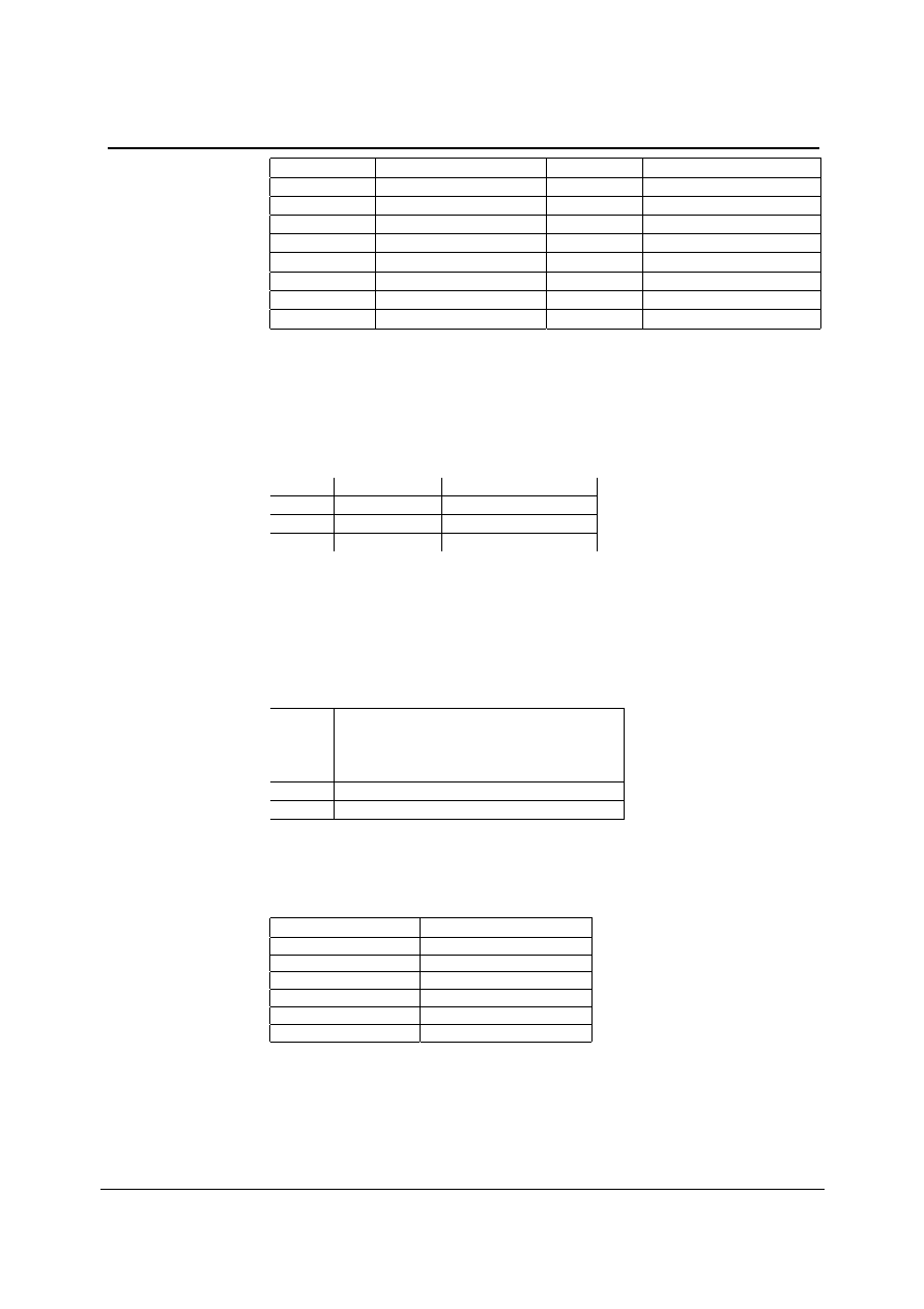
WM9705
Advance Information
AI Rev 3.6 October 2002
29
SR2 TO SR0
RIGHT RECORD SOURCE
SL2 TO SL0
LEFT RECORD SOURCE
0
Mic
0
Mic
1
CD in (R)
1
CD in (L)
2
Video in (R)
2
Video in (L)
3
Aux in (R)
3
Aux in (L)
4
Line in (R)
4
Line in (L)
5
Stereo mix (R)
5
Stereo mix (L)
6
Mono mix
6
Mono mix
7
Phone
7
Phone
Table 11 Record Select Register Function
RECORD GAIN REGISTERS (INDEX 1Ch)
1Ch sets the stereo input record gain with each step corresponding to 1.5dB. The MSB of the register
is the mute bit. When this bit is set to 1, the level for both channels is set at -
dB.
The default value is 8000h, which corresponds to 0dB gain with mute on.
MUTE GX3...GX0
FUNCTION
0
1111 +22.5dB
gain
0
0000 0dB
gain
1
xxxxx -
dB gain
Table 12 Record Gain Register Function
GENERAL PURPOSE REGISTER (INDEX 20h)
This register is used to control several miscellaneous functions of the WM9705.
Below is a summary of each bit and its function. Only the POP, 3D, MIX, MS and LPBK bits are
supported by the WM9705. The MS bit controls the Mic selector. The LPBK bit enables loopback of
the ADC output to the DAC input without involving the AC-link, allowing for full system performance
measurements. The function default value is 0000h which is all off.
BIT FUNCTION
POP
PCM out path and mute, 0 = pre-3D, 1 = post-3D
3D
3D stereo enhancement on/off, 1 = on
MIX
Mono output select 0 = Mix, 1 = Mic
MS
Mic select 0 = Mic1, 1 = Mic2
LPBK
ADC/DAC loopback mode
3D CONTROL REGISTER (INDEX 22h)
This register is used to control the centre and/or depth of the 3D stereo enhancement function built
into the AC'97 component. Only the depth bits DP0 to 3 have effect in the WM9705.
DP3...DP0 DEPTH
0 0%
1
-
8 Typical
value
-
15 100%
Table 13 3D Control Register
POWERDOWN CONTROL/STATUS REGISTER (INDEX 26h)
This read/write register is used to program power-down states and monitor subsystem readiness. The
lower half of this register is read only status, a 1 indicating that the subsection is ready. Ready is
defined as the subsection able to perform in its nominal state. When this register is written the bit
values that come in on AC-link will have no effect on read bits 0- 7.

WM9705
Advance Information
AI Rev 3.6 October 2002
30
When the AC-link Codec Ready indicator bit (SDATAIN slot 0, bit 15) is a 1 it indicates that the AC-
link and the WM9705 control and status registers are in a fully operational state. The AC'97 controller
must further probe this Powerdown Control/Status Register to determine exactly which subsections, if
any, are ready.
Note that the normal default condition of WM9705 when RESETB is applied is `all active'. However, if
pin MASK is pulled `hi' during RESETB active, all PR bits are overridden and the device enters a low
power mode. This allows a low power standby mode to be entered without writing to the device, a
condition that is desirable for example, if batteries are changed in a PDA. The state of the MASK pin is
latched on the rising edge of RESETB and if MASK is `hi' then the WM9705 will remain in low power
mode until register 26h is written to.
READ BIT
FUNCTION
REF
VREFs up to nominal level
ANL
Analogue mixers, etc ready
DAC
DAC section ready to accept data
ADC
ADC section ready to transmit data
Table 14 Powerdown Status Register Function
The Powerdown modes are as follows. The first three bits are to be used individually rather than in
combination with each other. The last bit PR3 can be used in combination with PR2 or by itself. PR0
and PR1 control the PCM ADCs and DACs only. PR6 powers down just the stereo Line Level output
headphone amps on pins 39/41.
The WM9705 also includes a low power DAC to headphone mode, whereby resetting PR1and PR6
enables the DAC and the path from the DAC to HPOUTL/R without having to power up the main mixer
(PR2). The POP bit (reg 20h) also needs to be set for this mode. The headphone amplifier on the
MONO output pin in not powered down by PR6, rather by PR2 or alternatively may be enabled by
setting MONOEN in register 74h.
WRITE BIT
FUNCTION
PR0
PCM in ADCs and input Mux Powerdown
PR1
PCM out DACs Powerdown
PR2
Analogue mixer Powerdown
(VREF still on)
PR3
Analogue mixer Powerdown (VREF off)
PR4
Digital interface (AC-link) Powerdown
(external clock off)
PR5
Internal clock disable
PR6
HP amp Powerdown
EAPD
External amplifier Powerdown
Table 15 Powerdown Control Register Function
PR0 = 1
PR1 = 1
PR2 = 1
PR4 = 1
PR0 = 0 AND
ADC = 1
DEFAULT
READY = 1
COLD RESET
WARM
RESET
PR2 = 0 AND
ANL = 1
PR1 = 0 AND
DAC = 1
ADCs OFF
PR0
DACs OFF
PR1
ANALOGUE
OFF PR2 OR
PR3
DIGITAL I/F
OFF PR4
SHUT OFF
CODA LINK
NORMAL
Figure 16 An Example of the WM9705 Powerdown/Powerup Flow

WM9705
Advance Information
AI Rev 3.6 October 2002
31
Figure 16 illustrates one example procedure to do a complete Powerdown of the WM9705. From
normal operation sequential writes to the Powerdown Register are performed to Powerdown the
WM9705 a piece at a time. After everything has been shut off (PR0 to PR3 set), a final write (of PR4)
can be executed to shut down the WM9705's digital interface (AC-link).
The part will remain in sleep mode with all its registers holding their static values. To wake up the
WM9705, the AC'97 controller will send a pulse on the sync line issuing a warm reset. This will restart
the WM9705's digital interface (resetting PR4 to 0). The WM9705 can also be woken up with a cold
reset. A cold reset will cause a loss of values of the registers, as a cold reset will set them to their
default states. When a section is powered back on, the Powerdown Control/Status Register (index
26h) should be read to verify that the section is ready (i.e. stable) before attempting any operation that
requires it.
PR0 = 1
PR1 = 1
PR4 = 1
NORMAL
ADC's OFF
PR0
DIGITAL I/F
OFF PR4
WARM RESET
PR0 = 0 AND
ADC = 1
PR1 = 0 AND
DAC = 1
SHUT OFF
CODA LINK
DACs OFF
PR1
Figure 17 The WM9705 Powerdown Flow with Analogue Still Active
Figure
17
illustrates a state when all the mixers should work with the static volume settings that are
contained in their associated registers. This is used when the user could be playing a CD (or external
LINEIN source) through WM9705 to the speakers but have most of the system in low power mode.
The procedure for this follows the previous except that the analogue mixer is never shut down.
The device can be used as a pen digitiser only, in order to set the WM9705 into this mode powerdown
bits PR3 to 0, PR6 and EAPD should be set.
Note that in order to go into ultimate low power mode, PR4 and PR5 are required to be set which turns
off the oscillator circuit. Asserting SYNC resets the PR4 and PR5 bit and re-starts the oscillator in the
same way as the AC link is restarted.
REGISTER 28h ≠ EXTENDED AUDIO ID
The Extended Audio ID register is a read only register that identifies which extended audio features
are supported (in addition to the original AC'97 features identified by reading the reset register at index
00h). A non zero value indicates the feature is supported.

WM9705
Advance Information
AI Rev 3.6 October 2002
32
DATA BIT
FUNCTION
VALUE
VRA
Variable rate audio support
1
DRA
Double rate audio support
0
SPDIF
SPDIF transmitter supported
`1' = supported
VRM
Variable rate Mic ADC support
0
DSA0
DAC slot mapping control
See table below
DSA1
DAC slot mapping control
See table below
CDAC
Centre DAC support
0
SDAC
Surround DAC support
0
LDAC
LFE DAC support
0
AMAP
Slot mapping support for Codec ID
1
REV0
Revision number
1
REV1
Revision number
0
ID0
Codec configuration ≠ pin 45 value
0 (Inverse of level at pin 45)
ID1
Codec configuration ≠ fixed in WM9705
0
Table 16 Extended Audio ID Register
DSA1, DSA0
DAC SLOT MAPPING
00
Slots 3 & 4
01
Slots 7 & 8
10
Slots 6 & 9
11
Slots 10 & 11
Table 17 DAC Slot Mapping
REGISTER 2AH ≠ EXTENDED AUDIO STATUS AND CONTROL REGISTER
The Extended Audio Status and Control Register is a read/write register that provides status and
control of the extended audio features. Note that SPDIF slot mapping default varies according to
codec pin configuration. See Table 2.
DATA BIT
FUNCTION
READ/WRITE
VRA
Enables variable rate audio mode
Read/write
SPDIF
SPDIF transmitter enable
Read/write
SPSA0
SPDIF slot assignment
Read/write
SPSA1
SPDIF slot assignment
Read/write
SPCV
SPDIF validity bit
Read
Table 18 Extended Audio Status and Control Register
SPSA0, SPSA1
DAC SLOT MAPPING
00
Slots 3 & 4
01
Slots 7 & 8
10
Slots 6 & 9
11
Slots 10 & 11
Table 19 SPDIF Slot Mapping
REGISTER 2Ch AND 32h ≠ AUDIO SAMPLE RATE CONTROL REGISTERS
These registers are read/write registers that are written to, to select alternative sample rates for the
audio PCM converters. Default is the 48ks/s rate. Note that only Revision 2.2 recommended rates are
supported by the WM9705, selection of any other unsupported rates will cause the rate to default to
the nearest supported rate, and the supported rate value to be latched and so read back. Sample rate
is entered in binary form to the appropriate register. Note sample rates should only be altered when
the relevant DAC or ADC is powered ON.

WM9705
Advance Information
AI Rev 3.6 October 2002
33
REGISTERS 3AH ≠ SPDIF CONTROL REGISTER
Register 3Ah is a read/write register that controls SPDIF functionality and manages bit fields
propagated as channel status (or sub-frame in the V case). With the exception of V, this register
should only be written to when the SPDIF transmitter is disabled (SPDIF bit in register 2Ah is `0').
Once the desired values have been written to this register, the contents should be read back to ensure
that the sample rate in particular is supported, then SPDIF validity bit SPCV in register 2Ah should be
read to ensure the desired configuration is valid. Only then should the SPDIF enable bit in register 2Ah
be set. This ensures that control and status information start up correctly at the beginning of SPDIF
transmission. WM9705 only supports an SPDIF sample rate of 48kHz.
CONTROL
BIT
FUNCTION
PRO Professional;
`0' indicates consumer, `1' indicates professional
AUDIB Non-audio;
`0' indicates data is PCM, `1' indicates non-PCM format (eg DD or DTS)
COPY Copyright;
`0' indicates copyright is not asserted, `1' indicates copyright
PRE Pre-emphasis;
`0' indicates not pre-emphasis, `1' indicates 50/15us pre-emphasis
CC[6-0]
Category code; programmed as required by user
L
Generation level; programmed as required by user
V Validity
bit;
`0' indicates frame valid, `1' indicates frame not valid
Table 20 SPDIF Control Register
VENDOR SPECIFIC REGISTERS (INDEX 5Ah - 7Ah)
These registers are vendor specific. Do not write to these registers unless the Vendor ID register has
been checked first to ensure that the controller knows the source of the AC `97 component.
MIXER MUTE PATH (INDEX 5Ah)
Bit 4 (MPM) is used to disable the path between the main input mixer and the lineout mixer, see Figure
9. Setting this bit to 1, breaks the connection and allows the following combinations:
DAC + PHONE + PCBEEP to line out / headphone out
DAC + CD + LINE + AUX + VID + MIC to mono output
When writing to this register all bits (except MPM) must be written as a 0 or device function can not be
guaranteed. Only the default value can be read from this register.
VENDOR SPECIFIC MODE CONTROL (INDEX 5Ch)
Register 5Ch is a vendor specific control register used to control the function of non-AC'97 specified
functions. This register defaults to all special features `disabled' i.e. All zeros.

WM9705
Advance Information
AI Rev 3.6 October 2002
34
CONTROL
BIT
FUNCTION
AMUTE
Indicates automute has been detected in the audio DAC (all `0' data) ≠ read only
HSCP
Headset detect comparator output ≠ read only
MPUEN
Mic pull up enable
MHPZ
Mono headphone tristate enable
PSEL
PHONE to MONO path switch enable
HSDT
Overrides Headset detect comparator, forcing left headphone amp to tristate
HSEN
Headset auto-detect enable
HPND
Headphone with no DAC enable
AMEN
Automute enable bit
I
2
S I
2
S data output enable
ADCNDAC
ADC no DAC path enable
ADCO
ADC to SPDIF and/or I
2
S output
HPF
ADC high pass filter disable;
HSCMP
Headset comparator enable bit
ASS1
ADC slot map control
ASS0
ADC slot map control
Table 21 Vendor Specific Control Register 5Ch
AMUTE indicates automute state has been detected. This is a read-only bit. 1 = automute detected.
HSCP is a read only bit, indicating headset detected. It is the output from the headset autodetect
comparator. 0 = headset detected.
MPUEN enables a 5mA (typ) pull up current on the MIC1 input pin, which when a headset
microphone of greater than 600R impedance is plugged in, causes the MIC1 pin to pull up to above
Vmid, and be detected. 1 = enable.
MHPZ tristates the MONO headphone driver output buffer. 1 = tristate.
PSEL enables the switch from PHONE input to MONO output; see block diagram. 1 = enable.
HSEN enables headset auto-detect function. HSCMP enables the headset detect comparator. 1 =
enable.
HSDT overrides the headset auto-detect comparator, forcing the left headphone output to tristate and
the HPLOUTL pin to be used as a headset microphone input path to the mic1 preamplifier input. 1 =
autodetect comparator override.
HPND enables the switch which outputs only the analog mixer output to the HPHONE outputs,
without the DAC signal being summed in. See block diagram. 1 = enable.
AMEN enables the DAC automute function, which detects zero data on both dac channels and auto-
mutes the outputs under this condition. 1 = enable.
Bit I
2
S enables I
2
S output, sending an LRCLK to the MASK/LRC pin (pin 43) and I
2
S data to the
SPEN/I
2
S pin (pin 44). BITCLK is used to clock out the data. Only 48ks/s data is supported. 1 =
enable.
ADCNDAC selects input to the ADC from before the point where the DAC signal is summed in. 1 =
select.
Bit ADCO is used to select data from the internal ADCs to be output as SPDIF or I
2
S data on these
pins rather than the data from the selected AC link slot. 1 = select.
HPF turns off the digital high pass filter in the ADC output when set to `1'.
ASS1, ASS0 are ADC slot mapping control bits. See table below. Default is slots 3 and 4.

WM9705
Advance Information
AI Rev 3.6 October 2002
35
ASS1, ASS0
ADC SLOT MAPPING ( L/R)
00
Slots 3 & 4
01
Slots 7 & 8
10
Slots 6 & 9
11
Slots 10 & 11
Table 22 ADC Slot Mapping Control
VENDOR SPECIFIC GAIN CONTROL REGISTER (INDEX 72h)
This register controls the gain and mute functions applied to the mixer path. This PGA is not
accommodated in the Intel specification, but is required in order to allow the option of simultaneous
recording of the mixer output and playback of DAC signals. The function is as for the other mixer
PGA's. However, the default value of the register is not-muted. If it is not used it will be transparent to
the user. Normally this reigster would be used in collaboration with bit ADCNDAC in register 5Ch,
allowing recording of the analog mix, manipulation in the digital domain by an external DSP, then
playback through the DACs on the W M9705.
PEN DIGITIZER CONTROL REGISTERS (INDEX 76, 78h)
These registers are used for pen digitiser control. See Pen Digitiser Operation section, for details of
operation.
PEN DIGITIZER DATA REGISTER (INDEX 7Ah)
Register 7Ah is used to store the results of digitizer ADC conversions, both for pen inputs and for
auxiliary input conversions. Results are downloaded to the controller by interrogating this register.
See Pen Digitiser Operation section for more details.
VENDOR SPECIFIC ADDITIONAL FUNCTIONALITY (INDEX 74H)
HPB boosts the headphone output by 6dB. 1 = 6dB boost enabled.
I2S64 enables a 64fs bitclk output on SPDIF for i
2
s data output. 1 = enabled.
MONOEN enables the mono output independently of PR2 (MIXER Powerdown). This allows the DAC
to MONOUT path to be powered up by resetting PR1 and setting MONOEN while the Mixer is
powered down (PR2 set), providing a lower power mode when the mixer function is not required.
VENDOR ID REGISTERS (INDEX 7Ch & 7Eh)
These registers are for specific vendor identification if so desired. The ID method is Microsoft's Plug
and Play Vendor ID code. The first character of that ID is F7 to F0, the second character S7 to S0,
and the third T7 to T0. These three characters are ASCII encoded. The REV7 to REV0 field is for the
Vendor Revision number. In the W M9705 the vendor ID is set to WML5.
Wolfson is a registered Microsoft Plug and Play vendor.

WM9705
Advance Information
AI Rev 3.6 October 2002
36
SERIAL INTERFACE REGISTER MAP
The following table shows the function and address of the various control bits that are loaded and read
through the serial interface.
Reg
Name
D15 D14 D13 D12 D11 D10 D9 D8 D7 D6 D5 D4 D3 D2 D1 D0 efault
00h Reset
X SE4 SE3 SE2 SE1 SE0 ID9 ID8 ID7 ID6 ID5 ID4 ID3 ID2 ID1 ID0 6150h
02h Master
volume Mute X
X ML4 ML3 ML2 ML1 ML0 X X
X MR4 MR3 MR2 MR1 MR0 8000h
04h HPHONE
volume Mute X
X ML4 ML3 ML2 ML1 ML0 X X
X MR4 MR3 MR2 MR1 MR0 8000h
06h Master
volume
mono
Mute
X X X X X X X X X X
MM4
MM3
MM2
MM1
MM0
8000h
0Ah
PCBEEP
volume
Mute
X X X X X X X X X X PV3
PV2
PV2
PV0
X
8000h
0Ch
Phone
volume Mute
X X X X X X X X X X
GN4
GN3
GN2
GN1
GN0
8008h
0Eh
Mic
volume Mute
X X X X X X X X
20dB
X
GN4
GN3
GN2
GN1
GN0
8008h
10h
Line in volume
Mute
X
X
GL4
GL3
GL2
GL1
GL0
X
X
X
GR4
GR3
GR2 GR1
GR0
8808h
12h CD
volume
Mute X
X GL4 GL3 GL2 GL1 GL0 X X
X GR4 GR3 GR2 GR1 GR0 8808h
14h
Video
volume Mute X X 0 1 0 0 0 X X X 0 1 0 0 0 8808h
16h
Aux
volume Mute X X 0 1 0 0 0 X X X 0 1 0 0 0 8808h
18h PCM
out
volume Mute X
X GL4 GL3 GL2 GL1 GL0 X X
X GR4 GR3 GR2 GR1 GR0 8808h
1Ah
Rec
select
X X X X X
SL2
SL1
SL0
X X X X X
SR2
SR1
SR0
0000h
1Ch
Rec
gain
Mute
X X X
GL3
GL2
GL1
GL0
X X X X
GR3
GR2
GR1
GR0
8000h
20h
General
purpose
POP X 3D X X X
MIX
MS
LPBK
X X X X X X X 0000h
22h
3D control
X
X
X
X
X
X
X
X
X
X
X
X
DP3
DP2
DP1
DP0
0000h
26h Power/down
control status
EAPD PR6 PR5 PR4 PR3 PR2 PR1 PR0 X X
X
X REF ANL DAC ADC 000Fh
28h Ext'd
audio
ID
ID1
ID0
X
X
REV1 REV0 AMAP LDAC SDAC CDAC DSA1 DSA0 VRM SPDIF DRA VRA 0605h
2Ah Ext'd
audio
stat/ctrl
X X X X X
SPCV
X
X X X
SPSA1
SPSA0
X
SPDIF
X
VRA
0000h
2Ch
Audio DAC rate
SR15
SR14
SR13
SR12
SR11 SR10 SR9
SR8
SR7
SR6
SR5
SR4
SR3
SR2
SR1
SR0
BB80h
32h Audio
ADC
rate SR15 SR14 SR13 SR12 SR11 SR10 SR9 SR8 SR7 SR6 SR5 SR4 SR3 SR2 SR1 SR0 BB80h
3Ah
SPDIF
control V 0 1 0 L
CC6
CC5
CC4
CC3
CC2
CC1
CC0
PRE
COPY
AUDIB
PRO
2000h
5Ah
Mixer Path Mute
0
0
0
0
0
0
0
0
0
0
0
MPM
0
0
0
0
0000h
5Ch Add.
Function
control
AMUTE HSCP MPUEN MHPZ PSEL HSEN HSDT HPND AMEN I
2
S ADCN
DAC
ADCO HPF HS
CMP
ASS1 ASS0 0000h
72h Front
mixer
volume
Mute X
X GL4 GL3 GL2 GL1 GL0 X X
X GR4 GR3 GR2 GR1 GR0 0808h
74h
Add.
Function X X X X X X X X X X X X HPB
I2S64
X
MONOEN
0000h
76h Digitizer
control POLL ADR2 ADR1 ADR0 COO CTC CR1 CR0 DEL3 DEL2 DEL1 DEL0 SLEN SLT2 SLT1 SLT0 0006h
78h Digitizer
control PRP1 PRP0 RPR PDEN PINV BSEN
BINV
WAIT PIL PHIZ MSK1 MSK0 PDD3 PDD2
PDD1 PDD0 0000h
7Ah
Pen Digitizer data PNDN
ADR2 ADR1 ADR0
D11
D10
D9
D8
D7
D6
D5
D4
D3
D2
D1
D0
0000h
7Ch
Vendor
ID1
F7 F6 F5 F4 F3 F2 F1
F0 S7
S6 S5 S4 S3 S2
S1 S0
574Dh
7Eh
Vendor
ID2
T7 T6 T5 T4 T3 T2 T1
T0
Rev7
Rev6
Rev5
Rev4
Rev3
Rev2
Rev1
Rev0
4C05h
Table 23 Serial Interface Register Map Description
Note:
1.
Default values of register 28h and 2Ah depend on whether the device is a primary or secondary, and whether SPDIF capability is
enabled by pulling pin 44 SPEN high. The conditions shown are for a primary codec with SPDIF capability.
2.
Register 5Ah is write only. When writing to this register all bits except MPM (bit 4) must be written as 0, otherwise device
function can not be guaranteed.

WM9705
Advance Information
AI Rev 3.6 October 2002
37
PEN DIGITISER OPERATION
The pen digitiser function comprises a 12 bit successive approximation ADC, with a multi-channel
input multiplexor to select which signal to convert, and a switching matrix to control driving of signals to
the resistive touchscreen plates. A finite state machine is provided in order to control and sequence
conversion operations.
A pen-down detection scheme is provided to allow detection of when the pen is in contact with the
screen. This allows for the touchscreen to only be driven whilst the pen is down, saving on
unnecessary power consumption. This minimises any degradation in audio performance that may
occur due to the significant currents that flow through the on-chip screen drive switches. Figure 18
shows symbolically these component elements and their connectivity.
ADC ip Mux
Rscrx
Rscry
Rpen
Y+
Y-
X+
X-
12 bit
SAR
ADC
Vref+
Vref-
Y+
X+
Y-
X-
PHONE
PCBEEP
AUXADC
BMON
AUX
input
MUX
PDRES
PENDET
BUSY
12 bit op
Rpusw
Xswp
Xswn
Yswn
Pressure switch
Rpu
Pen Controller
State machine
and AC link
interface
MASK
Switch control
ADC control
Pen detect
comparator
Vref+ switches
Vref- switches
Ipress
Yswp
Vrswap
Vrswyp
Vrswxp
Vrswxn
Vrswyn
Vrswan
MXxp
MXyn
MXxn
MXaux
MXyp
Prsw
Figure 18 Pen Digitiser Block Diagram
Y+
X+
X-
Y-
Rpen
A/D
converter
Vrswyn
Vrswyp
Yswn
Yswp
MXxp
MXxn
Figure 19 Y Position Conversion
Y+
X+
X-
Y-
Rpen
A/D
converter
Vrswxn
Vrswxp
Xswn
Xswp
MXyp
MXyn
Figure 20 X Position Conversion

WM9705
Advance Information
AI Rev 3.6 October 2002
38
TIMING OF PEN DIGITISER OPERATIONS
Timing of pen digitiser operations is linked to the AC link frame timing. A single ADC conversion takes
one frame to complete, including taking a sample, converting it, and passing it into the register ready to
be read back. This therefore allows a maximum conversion rate of 48ks/s, but in practise to allow time
for screen plates to settle etc, much lower rates of conversion are anticipated.
The ADC is powered up only for the duration of each conversion, therefore power consumption is a
linear function of the conversion rate chosen.
CONTROL OF PEN DIGITISER FUNCTIONS
Control of the digitiser functions is via control bits written into control registers via the AC link. The
following table shows the name, function and location of the control bits for the pen digitser section of
the WM9705. Address locations are chosen to avoid unexpected corruption of normal AC'97 audio
codec operation, using mostly vendor specific addresses from the AC'97 adddress map.
Reg
Name
D15
D14
D13
D12
D11
D10 D9 D8 D7 D6 D5 D4 D3 D2 D1 D0 efault
76h Digitizer
control
POLL ADR2 ADR1 ADR0 COO CTC CR1 CR0 DEL3 DEL2 DEL1 DEL0 SLEN SLT2 SLT1 SLT0 0006h
78h Digitizer
control
PRP1 PRP0 RPR PDEN PINV BSEN BINV WAIT PIL PHIZ MSK1 MSK0 PDD3 PDD2 PDD1 PDD0 0000h
7Ah
Pen
Digitizer
data PNDN
ADR2
ADR1
ADR0
D11 D10 D9 D8 D7 D6 D5 D4 D3 D2 D1 D0 0000h
INDEX 76H ≠ DIGITISER CONTROL WORD 1 ≠ READ/WRITE REGISTER
BIT LOCATION
FUNCTION
POLL
15
Starts a single polled conversion (resets itself at completion)
ADR[2-0]
14-12
Sets the address of the single conversion in polled mode, or extra conversions in Co-
ordinate or Continuous mode. See Table 24.
COO
11
Selects a co-ordinate set of conversions
CTC
10
Starts continuous conversion operation
CR[1-0]
9,8
Sets continuous conversion rate
DEL[3-0]
7-4
Sets the delay between screen being driven and X or Y sample being taken
SLEN
3
Slot enable bit; allows conversion results to be output onto chosen slot
SLT[2-0]
2-0
Slot select bits; choose which slot to output data results in

WM9705
Advance Information
AI Rev 3.6 October 2002
39
INDEX 78H ≠ DIGITISER CONTROL WORD 2 ≠ READ/WRITE REGISTER
BIT LOCATION
FUNCTION
PRP[1:0]
15:14
Pen digitiser power down bit control bits:
00 ≠ Pen digitiser powered down, pen detect disabled, no wakeup on pen down (default)
01 ≠ Pen digitiser powered off, pen detect enabled, wakeup on pen down enabled
10 ≠ Pen digitiser powered off, pen detect enabled, no wakeup on pen down
11 ≠ Pen digitiser powered up
RPR
13
Enables PR4 reset on pen down wake up
PDEN
12
causes conversions and screen drives to stop when pen is not down
PINV
11
Inverts sense of PENDET output: Default `0' causes PEN = `down' to give a `1' output
BSEN
10
BUSY flag enable. Outputs converter BUSY signal on pin 47. `1' = converter busy, goes low
at end of conversion to indicate result available
BINV
9
Invert sense of BUSY flag output
WAIT
8
WAIT bit; setting this bit causes conversion operations to halt when a result is about to be
written to the data register 7Ah, if the last stored result has not yet been read. Conversions
commence again once the result has been read
PIL
7
Pressure current select (`0'=200uA, `1'=400uA)
PHIZ
6
Sets PHONE and PCBEEP inputs to be High impedance ( disconnects from mixer). The
default sate of this bit is low which corresponds to the switch being open.
MSK[1:0]
5:4
Selects what effect MASK input has:
00 = MASK pin ignored
01 = Mask pin is static; `hi' halts conversions
10 = Mask pin is edge sensitive; rising or falling edge delays conversions by DEL [3-0]
11 = Mask pin becomes a synchronise input; conversions happen after edge
PDD[3:0]
3:0
Pen detect comparator threshold
0 to Vmid in 15 steps; 0h = use zero power comparator with Vmid threshold
1 = Vmid/15 threshold
15 = Vmid threshold
INDEX 7AH ≠ DIGITISER DATA WORD OUTPUT ≠ READ REGISTER ONLY
BIT LOCATION
FUNCTION
PNDN
15
Indicates whether Pen is Down; `1' = `Down'
ADR[2:0]
14:12
Conversion Address; Indicates which channel the following result is for
D[11:0]
11:0
ADC output result
READBACK OF PEN DIGITISER RESULTS
Readback of conversion results from either pen co-ordinate conversions, pressure measurements, or
auxiliary conversion, is via the AC link interface.
Readback may be performed either by reading from the read only register 7Ah via the AC link, or by
enabling SLOT mode (by writing SLEN = 1 in register 76h) where results are placed into the AC link
data slots by WM9705, and sent back to the controller.
The readback word contains the 12 bit data in the lsb locations, plus a 3 bit header in the next 3 bit
locations, whose value corresponds to the channel that the data was converted from. Other bits are
padded with zero values. Channel addressing is the same as the address requested for the
conversion, as follows:

WM9705
Advance Information
AI Rev 3.6 October 2002
40
ADR[2-0] CHANNEL
000 none
001 X-
plate
010 Y-plate
011 Pressure
Conversion
100 BMON
101 AUXADC
110 PHONE
111 PCBEEP
Table 24 Conversion Address to Channel Map
If BUSY flag is enabled (BSEN bit in reg 78h set `1') then the BUSY pin will remain high until the
conversion in complete, whereby it will transition low.
This signal is output onto pin 47, EAPD/BUSY where it may be observed by the controller if required
as an interrupt. (Note that use of this BUSY flag clearly precludes use of the EAPD external amplifier
power down bit, but as the WM9705 has integrated headphone amplifier with it's own power down bit
PR6 in register 26h, this should not be a problem. If BSEN is not set, then EAPD operates as normal)
If SLOT method is enabled (SLEN bit in register 76h is set `1') then the data is output into the chosen
slot and the appropriate slot tag bit set. Choice of which slot the data is written into is made by setting
bits SLT[2-0] in register 76h. The following table shows which slot versus [2-0] value.
SLT[2-0]
OUTPUT SLOT FOR
DIGITISER DATA
000 5
001 6
010 7
011 8
100 9
101 10
110 11
Table 25 Pen ADC Slot Select
When the conversion result has been read, then another conversion may be commenced as required.
In the event of another conversion being requested, then the stored result from the last conversion will
be overwritten when the new conversion has been completed.
However, if the WAIT bit is set in register 78h, then once a conversion is complete, the current
conversion result may not be written into the results register, until the previous conversion result has
been read. The sequence will halt at the finish of this current conversion, waiting for the results
register to be cleared. Note that this does allow the controller to slow down the rate of conversions, so
effectively determining the overall rate of conversion.
CONVERSION CONTROL
Control of ADC conversions, and screen driving functions, is by one of three methods:
∑
Polling
method
∑
Polled Co-ordinate method
∑
Continuous
method

WM9705
Advance Information
AI Rev 3.6 October 2002
41
POLLING METHOD
The polling method relies on the controller to instruct every operation, i.e. to send an instruction
requesting every individual conversion specifically. A polled conversion is requested by writing a 1 to
POLL bit 15 in register 76h, along with the address of the channel to be converted.
The channel to convert is identified by a 3-bit tag word ADR[2-0] written to the Pen control register
76h. This tag has the same value as the value read back with the conversion result, thus identifying
which channel the result is for, see Table 24. If ADD[2-0] is set to 0 then no conversion will take place
and POLL will be reset.
If the channel to convert is an X or Y pen channel, then the appropriate screen driver switch
configuration is selected first, the screen allowed to settle for a time (selected by programming the
value into the DELAY register, DEL[3-0] in register 76h) and then the screen sample taken and the
conversion made. Figures A2 and A3 show the switch configurations for X and Y plate conversions.
Once the conversion is complete, the result is written into the results register 7Ah where it is available
for readback.
Figure 21 Control of ADC conversions : Polling Method
CO-ORDINATE METHOD
Setting bit COO in register 76h puts the device into Co-ordinate conversion mode.
Co-ordinate method of conversion instructs a sequence of conversions necessary to perform a pen
co-ordinate determination. Most basically this requires an X and a Y conversion but may also include a
pressure measurement. Writing to the POLL bit with COO bit in register 76h set initiates a set of co-
ordinate conversions, the results of which are returned to the controller as soon as they are available.
If pressure conversion, or an auxiliary conversion are also required as part of the sequence, this is
instructed by writing the appropriate address into the ADR [2-0] bits of register 76h. (X and Y
addresses do not need to be set in this case, as they are implied by the choice of co-ordinate method
of operation). DEL[3-0] delays are applied as for polled operation to all conversions. Subsequent POLL
operations will then return both X and Y conversion results, plus the auxiliary or pressure conversion
result indicated by the value set in ADR[2-0].
Once a conversion is complete, the result is written into the results register 7Ah where it is available
for readback.
Screen Switch
/ Input Mux
mode
EAPD/BUSY
delay = 2 frames
Single coordinate conversion with ADR = 000 (X and Y only) with delay set to 1 (2 frames)
POLL
SYNC
ADR = 001 - X measurement
ADR = 010 - Y measurement
DELAY
CONVERT
DELAY
CONVERT
ADC MODE
Pen Detect or Off
X
X
Write to 0x76 with 0x8810
SDOUT
Pen Detect or Off
delay = 2 frames
PENDATA
X
X measurement data
Y measurement data
external signals
internal signals
WM9705
Advance Information
AI Rev 3.6 October 2002
42
Figure 22 Control of ADC conversions : Polled Co-ordinate Method
Note:
The pressure measurement is the difference between the voltage values measured between the
resistive plates in the screen. As two values have to be obtained before the calculation can take place,
two data acquisition cycles are required as illustrated above.
Screen Switch
/ ADC mux
mode
Different types of polled conversion with delay set to 0 (1 frame)
POLL
SYNC
ADR=1
DELAY
CONVERT
ADC MODE
X
Write to 0x76
with 0xB800
SDOUT
PENDATA
Poll = 1, Coord = 0, ADR = 001 ( 0x76 = 0x9000 ) = X Measurement
DELAY
CONVERT
ADR=2
DELAY
CONVERT
ADR=3(1)
1
DELAY
CONVERT
ADR=3(2)
1
X Measurement
Y Measurement
Pressure
Measurement
POLL
ADR=1
DELAY
CONVERT
ADC MODE
X
Write to 0x76
with 0x9000
PENDATA
X Measurement
Coord = 1, ADR = 011 ( 0x76 = 0xB800 ) = X, Y and Pressure
SDOUT
POLL
ADR=1
DELAY
CONVERT
ADC MODE
X
Write to 0x76
with 0xD800
SDOUT
PENDATA
DELAY
CONVERT
ADR=2
DELAY
CONVERT
ADR=5
X Measurement
AUX Measurement
Coord = 1, ADR = 101 ( 0x76 = 0xD800 ) = X, Y and AUX
Y Measurement
Screen Switch
/ ADC mux
mode
Screen Switch
/ ADC mux
mode

WM9705
Advance Information
AI Rev 3.6 October 2002
43
CONTINUOUS METHOD
The continuous method of conversion allows for an autonomous free running operation of the digitiser,
converting pen X,Y results and either pressure or AUX channels continuously at a pre-set rate. This
removes from the controller the overhead associated with instructing which conversion to do next etc.
Continuous conversion is enabled by setting the CTC bit in register 76h. The rate of operation of the
conversion sequence is set by writing bits CR0/1 into register 76h. These set the sequence rate as
follows:
CR1 CR0
CONVERSION
RATE
0
0
93.75Hz or 512 AC link frames
0
1
187.5Hz or 256 AC link frames
1
0
375Hz or 128 AC link frames
1
1
750Hz or 64 AC link frames
Table 26 Conversion Rate
Note that this rate is the MAXIMUM that may be obtained. In practice the rate will typically be slower, if
the number of conversions to be performed, and the delay applied by the DEL[3-0] bits to each
conversion, add up to a time greater than the nominal period for conversion set above. Likewise, if
conversions are halted by pen going up, or MASK being applied, then this conversion rate will not be
met. If MSK[1,0] is set to 11, then the conversion rate becomes synchronised to the rate of application
of edges to the MASK input. The CR[1,0] value is ignored. Conversions are performed after the edge
on the MASK pin, delayed by the value set in the DEL [3-0] register.
Normal operation will be to perform X,Y screen drives, and conversions, followed by a pressure or
AUX conversion if requested by setting the appropriate address in the ADR[2-0] bits of register 76h.
So long as the ADR[2-0] value remains set to auxiliary or pressure inputs, X,Y and the extra auxiliary
conversions will be made in every cycle.
Pen-down detection is performed after completion of each set of conversions and the output sent to
the PENDET pin, and output in bit 15 of the data read-back word. If the PDEN bit is left at the default
value `0', if pen-down is not detected, then the continuous conversion process including driving the
screen, will continue anyway. If the PDEN bit is set to `1', and a pen-down is NOT detected, then the
conversion process will come to a stop, until the pen is once more returned to the screen. DEL[3-0]
delays are applied as for polled operation to all conversions.
Once a conversion is complete, the result is written into the results register 7Ah where it is available
for readback. Additionally the results may be output into a chosen SLOT by enabling slot readback bit
SLEN in register 76h and selecting the desired slot by setting SLT[2-0].
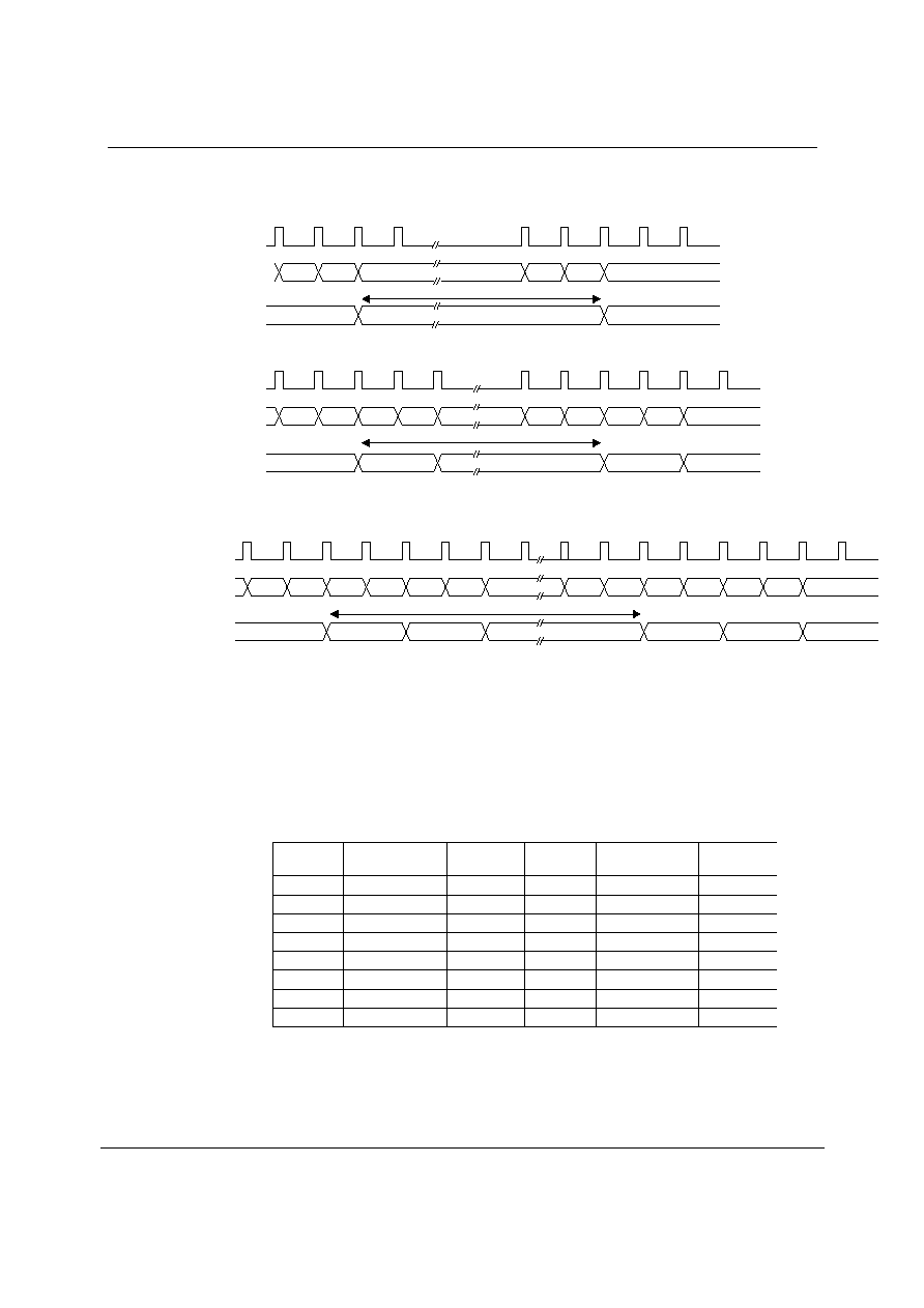
WM9705
Advance Information
AI Rev 3.6 October 2002
44
Figure 23 Control of ADC conversions : Continuous Method
DELAY FUNCTION
In order to allow time for the plates to charge to a steady voltage when the screen drive switches are
closed, a programmable delay may be applied which delays the sampling of the appropriate plate
voltage by the ADC. This delay is at least one frame (1/48kHz) in duration, but may be increased by
writing a value to the DEL[3-0] bits in register 76h. These set delays as follows:
DEL[3-0] DELAY
(FRAMES)
DELAY
(uS)
DEL[3-0] DELAY
(FRAMES)
DELAY
(uS)
0 1
20.8
8 96
1666
1 2
41.7
9 128
2000
2 4
83.3
10
160
2333
3 8
166.7
11
192
2666
4 16
333.3
12
224
3000
5 32
666.7
13
256
3333
6 48
1000
14
288
3666
7 64
1333
15
infinite infinite
Table 27 Programmable Screen Drive Delay
Note that code 15 is used as a special mode, where the plates are driven permanently on, the switch
matrix setting controlled by the value selected by ADR[2-0]. Thus the plates may be permanently set to
drive X screen, Y screen, pressure configuration, or the auxiliary input channel permanently connected
to the ADC input. For further information please see the section on Auxiliary Conversions.
Different types of continuous conversion with delay set to 0 (1 frames)
CTC = 1, CC=11, Coord = 0, ADR = 001 ( 0x76 = 0x1700 ) = X Measurement every 64 AC Link Frames
DELAY
CONVERT
Conversion 1 result available
DELAY
CONVERT
Conversion 2 result available
Conversion 1
Conversion 2
64 Frames
CTC = 1, CC=00, Coord = 1, ADR = 000 ( 0x76 = 0x0C00 ) = X and Y Measurement every 512 AC Link Frames
DELAY
CONVERT
Conversion 1 - X
result available
DELAY
CONVERT
Conversion 1
Conversion 2
512 Frames
CONVERT
DELAY
CONVERT
DELAY
Conversion 2 - X
result available
Conversion 2 - Y
result available
CTC = 1, CC=01, Coord = 1, ADR = 100 ( 0x76 = 0x4C01 ) = X, Y and BMON Measurement every 256 AC Link Frames
DELAY
CONVERT
Conversion 1
256 Frames
CONVERT
DELAY
CONVERT
DELAY
Conversion 1 - Y
result available
Conversion 2 - X
result available
DELAY
CONVERT
Conversion 1
256 Frames
CONVERT
DELAY
CONVERT
DELAY
Conversion 2 - Y
result available
Conversion 2 - BMON
result available
Conversion 1 - BMON
result available
SYNC
ADC Mode
Pen Data
ADC Mode
SYNC
Pen Data
ADC Mode
Pen Data
SYNC
Conversion 1 - Y
result available
Conversion 1 - X
result available

WM9705
Advance Information
AI Rev 3.6 October 2002
45
BUSY SIGNAL
The BUSY signal is derived from the pen state machine and is an indication of the AUXADC being
active on a conversion cycle. When an AUXADC conversion is requested BUSY will go high 61
BCLKs after the rising edge of SYNC in the frame that the conversion was requested. BUSY will
remain high until the data from the conversion is written into register 7A as the state machine sees the
register write as the last stage of the conversion.
During a conversion that does not have the WAIT bit set, the BUSY negative pulse between
conversions (signifying data written to Reg 7Ah) lasts 3 BCLKs and starts 11 BCLKs before the next
rising SYNC edge. At the end of a conversion (or set of conversions) BUSY goes low 11 BCLKs
before SYNC rises.
The WAIT bit instructs the device to wait until the previous conversion result has been read from
register 7Ah before overwriting it. Without this bit set conversion results are not held. During a multiple
conversion cycle in which WAIT is set the busy signal may operate differently. If the device it set to
perform 3 simultaneous conversions with WAIT set the timing of busy is dependant on when the
results are read from register 7A. If at the end of conversion 2 the result from conversion 1 has not
been read from the register the conversion sequence can not complete. In this case BUSY will remain
high until 61 BCLKs after the rising SYNC edge at the beginning of the frame in which register 7A was
read. However if the result is read from register 7A before the end of conversion 2 the busy signal will
operate as described in the paragraph above.
In the case of single conversions with WAIT set the operation of BUSY would be the same as that
described above if the data was not read from Reg 7Ah before the next conversion requested had
completed.
PRESSURE MEASUREMENT
Pen pressure is implied by determining the resistance between the two plates.
Pressure measurements are sometimes used to determine whether the pen is in contact with the
screen. However in this system the pen-down detect method is a far less power hungry way of
determining whether the pen is `down' as it does not require continuous driving of the screen and ADC
conversions. This has the supplemental benefit of minimising audio signal interference. Pen pressure
measurements may be made if required, perhaps for reasons other than simply determining pen-
down.
This is done by injecting a known current into one end of one of the two plates (Y+), and grounding
one end of the other plate (X-). Then the voltage at the other two plate terminals is converted (Y- and
X+), the difference being a direct measure of the injected current value multiplied by the Pen contact
resistance. Figure A4 shows this schematically.
Requesting a pressure measurement automatically initiates a pair of conversions, the difference in
conversion values being returned as the pressure measurement. Delay between switching the
appropriate screen and ADC mux switches, and performing the conversions, is set in the DEL[3-0]
registers.
Figure 24 Pressure Measurement
Y+
X+
X-
Y-
Rpen
A/D
converter
Vrswxn
Vrswyp
Xswn
Yswp
MXyp 1st conv
MXyn 2nd conv
Prsw
Ipress
Yswp
Vrswap
Vrswan

WM9705
Advance Information
AI Rev 3.6 October 2002
46
MASK FUNCTION
It is anticipated that sources of glitch noise such as LCD `invert' signals will likely be picked up by the
touchscreen plates and affect measurement accuracy. In order to minimise this effect, a signal may be
applied to the MASK pin, which depending on the setting of the MSK[1-0] bits in register 78h, will
delay the start of sampling of any input to the ADC. The behaviour of this delay is a function of the
value set in the MSK[1-0] bits of register 78h and is described below:
MSK[1-0]
EFFECT OF SIGNAL ON MASK PIN
00
Mask has no effect on conversions
01 Static;
`hi' on MASK pin stops conversions, `lo' has no effect.
10
Edge triggered; rising or falling edge on MASK pin delays conversions
by an amount set in the DEL[3-0] register. Conversions are asynchronous to the
MASK signal.
11
Synchronous mode; conversions wait until rising or falling edge on MASK
initiates cycle; screen starts to be driven when the edge arrives, the conversion
sample being taken a period set by DEL[3-0] after the edge.
Table 28 Mask Control
PEN-DOWN DETECTION
Pen down detection is an important feature of the pen digitiser function; it allows screen driving and
conversion operations to be suspended whilst the pen is not in contact with the screen so conserving
power and minimising audio signal interference due to screen currents.
Pen down detection is performed by connecting an external or internal Pen Down Pull-up resistor
(external resistor is connected between pin 29 and AVdd) to the Y+ terminal of the screen, grounding
the X- terminal, and connecting the Y+ terminal to a comparator. This comparator has a threshold
which lies midway between the ground and AVdd voltages. When the pen is applied to the screen, the
resistance between the plates falls, pulling down the voltage on the Y plate and hence the Y+ terminal
voltage. W hen this resistance falls enough, the comparator is triggered, so detecting that the `pen is
down'.
The threshold of this Pen detection function is set at about midrail. Varying the pressure on the pen,
hence the pen resistance between the shorted plates, will cause the voltage on the pulled-up plate to
vary. The value of the external pull up resistor may be selected, so allowing the sensitivity of the pen-
down detect threshold to be adjusted. This allows the user more flexibility in tailoring the pen detect
threshold to different screen types.
A `zero power' comparator (effectively a gate) is used as the comparator, which has a fairly crudely set
threshold, set at about mid supply. The output of this comparator is applied to the PENDET pin, and
also into the finite state machine controlling the conversion and screen drive operations. Depending on
the state of the PDEN bit in register 78h, this signal may be used to halt conversion operations whilst
pen is `up'. The PENDET pin can be active high or low depending on the state of PINV. The default
state of PINV is a 0 which means PENDET is active high.
If the PDEN bit has not been set, then the state of the pen down detector output enables conversions
and screen drives only when the pen is detected as `down'. If PDEN bit is set, then conversions and
screen drives will continue whether pen is detected as up or down. This allows, for example, for AUX
channels to be converted whilst the pen is off the screen.
In order to provide more control over the sensitivity of the pen down detect threshold, an alternative
active comparator circuit is provided, along with a 4 bit DAC which is used to adjust the comparator
reference input voltage between near 0Volts and midrail. This allows lower pen resistance to be
detected, without the need to use very low external pull-up resistor values which would otherwise be
needed and which would consume large currents. When value 0h is written to the pen detect dac
register bits PDD[3-0] in register 78h, this extra comparator is powered off and the zero power
comparator used. When other values are written to this register, then the comparator is enabled, and
thresholds from near 0V to midrail are set as below in Table 29.
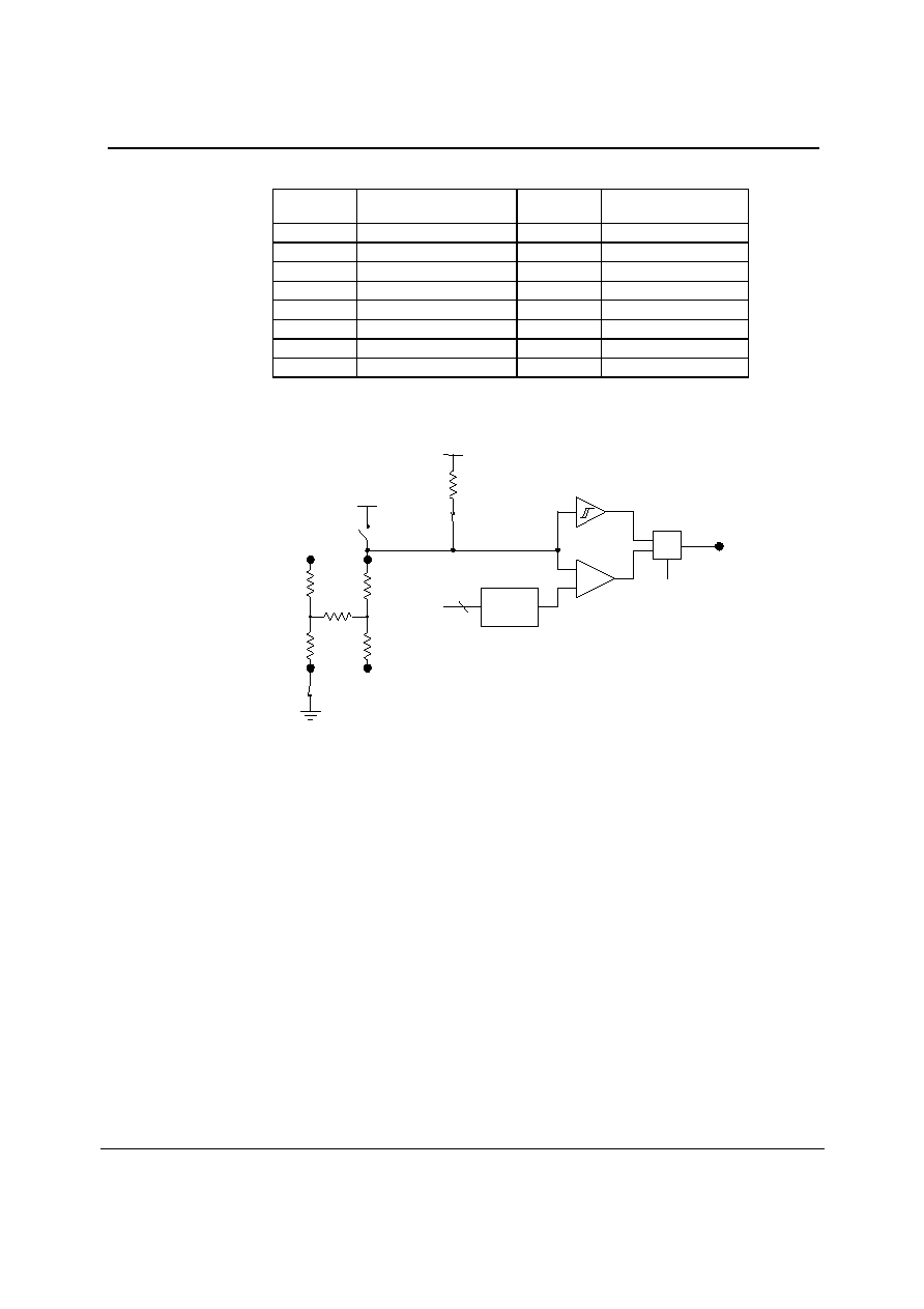
WM9705
Advance Information
AI Rev 3.6 October 2002
47
PDD[3-0] PEN
DETECT
THRESHOLD
PDD[3-0] PEN
DETECT
THRESHOLD
0000
Use zero power comp.
1000
8Vmid/15
0001 Vmid/15
1001 9Vmid/15
0010 2Vmid/15
1010 10Vmid/15
0011 3Vmid/15
1011 11Vmid/15
0100 4Vmid/15
1100 12Vmid/15
0101 5Vmid/15
1101 13Vmid/15
0110 6Vmid/15
1110 14Vmid/15
0111 7Vmid/15
1111 Vmid
Table 29 Pen Detect Comparator Threshold
Figure 25 shows the pen detection function schematically.
Y+
X+
X-
Rpen
Xswn
Yswp
Rpusw
Rpu
Pen detect
threshold
setting DAC
4 bit
mux
sel
PENDET
zero power comparator
precision comparator
Y-
Figure 25 Pen Detection Configuration
STANDBY OPERATION AND WAKE-UP
WM9705 allows for complete zero power standby operation, and wake-up-on-pen-down.
That is, all features of the device can be put into zero quiescent current standby, including the digital
interfaces, and the device will wait consuming near zero power until it is re-awoken via pen down event
or via activity on the AC link.
The AC link interface specification allows for standby operation, with all clocks stopped and the
oscillator powered down, (all PR bits set). From this state, either the controller or the Codec can re-
awaken the AC link. This feature is used by WM9705 to allow the standby operation, and wake on pen
down function.
Once in standby, (all PR bits set and Pen digitiser power down control bits PRP{1:0] in reg 78h set
to), the device awaits detection of pen down. Once this occurs, PRP[1] is set to active (1) and the pen
digitiser wakes up, toggles the PENDET pin, and wakes the AC link by toggling the SDATAIN line. It
is then up to the link controller how to respond. It will then toggle the SYNC signal, which causes the
codec to wake up the AC link by re-setting PR4, waking the oscillator and starting to send BITCLKs. If
RPR is set then pen down will also automatically reset PR4 and wake up the codec.
If the PRP[1:0] is set to 10, then the device is NOT woken on pen down detect, but the PENDET flag
is toggled on pin 46 when the pen is detected as `down'. The controller may then wake up the AC link
and hence set PRP[1] bit if it so wishes.

WM9705
Advance Information
AI Rev 3.6 October 2002
48
Setting PRP[1:0] to 00 will power off the digitiser and and pen down detection. PENDET will not toggle
on pen down.
Provision of the PENDET flag as well as the the AC link wake up procedure allows controllers that
might not be full AC link compliant to still operate in this way, by monitoring the change in state of
PENDET and using that signal as a wake-up flag.
AUXILIARY CONVERSIONS
As previously described, auxiliary conversion may be performed by setting the ADR[2-0] address to
the chosen input pin. Two completely dedicated input pins, AUXADC and BMON, and 2 shared
inputs (PHONE, PCBEEP) may be selected as inputs to the ADC. The PHONE and PCBEEP inputs
are normally still available as regular analogue inputs to the mixer path, and as such present a typical
100k input impedance (with respect to mid-rail). However, in the event that these analogue inputs are
not required, and there is a need to use these inputs as high impedance auxiliary inputs, then setting
bit 6, PHIZ, in register 78h disconnects the internal PHONE and PCBEEP paths, so making these
inputs into high impedance ADC inputs only. The signal paths from PHONE or PCBEEP to the
MIXER are disconnected in this mode.
Inputs to the AUXADC input should never exceed supply rails.
The ADC uses the AVDD1 and AGND1 supplies as it's references, therefore conversions of
AUXADC or BMON inputs are ratioed to these supplies; if they are inaccurate then the conversion
may be inaccurate in absolute values.
If co-ordinate (COO set) or continuous (CTC set) conversion modes are chosen, then auxiliary
conversions are performed amongst the cycle of screen drives and conversions.
In POLL (POLL set) mode, single auxiliary conversions may be performed. This cycle may be
repeated to allow relatively high conversion rates to be applied to a single channel if required.
In this case, setting the DEL[3-0] value to 15, and the ADR[2-0] value to the required channel will
permanently connect that channel input to the ADC input. In this way maximum cycle time for
conversion may be achieved, by instructing POLL and reading the ADC result on alternate AC link
frames. This gives a maximum conversion rate of 24k samples per second from 1 channel.
Alternatively continuous mode (CTC = `1') may be used to automatically generate conversion samples
a the highest rate. The conversion rate control bits CTR[1-0] will limit this rate unless DEL[3-0] is set
to 15. Then CTR[1-0] sets conversion rates of 1, 2, 4, 6 frames per sample. In this case up to one
conversion is made per AC link frame, giving sample rates of 8, 12, 24 or 48ks/s. It is recommended
that in this case the SLOT method of transferring data is used.
Inputs to the BMON battery monitoring input are allowed to be more positive than the AVdd supply rail,
up to a maximum of 6.5Volts (total). This allows a battery of voltage greater than the AVdd supply to
be monitored by the ADC without need for an external resistive divider. An internal divide by three
consisting of a 20k and a 10k resistor in series, is switched onto the BMON pin whenever a
conversion on this input is requested. Therefore current is consumed from the BMON input during the
battery monitoring conversion process, but not at any other time. A series switch disconnects the
divider from the negative internal supply when conversions are not being requested. Because of the
internal divide by 3, inputs to the BMON pin are therefore converted with a digital output gain 1/3
rd
that
of the other AUXADC input
The input impedance of the BMON input is 30k to ground WHEN the ADC is sampling, or hi-Z when
it's not. When a BMON sample is requested the ADC samples the battery for a minimum of two
frames. Inherent in this conversion is the delay state, set in register 7h bits 4-7 (DEL [3:0]), the lowest
value of this delay is 0 which will introduce a delay of one frame, thus the minimum number of 2
frames for a conversion. If the BMON conversion is part of a set of conversions the delay state set for
the series of conversions will be inherited by the BMON conversion. The minimum time the battery can
see the 30k is 512 BCLKs or 41.6 us.
In order to have an equivalent resistance of greater than 1M ohms the battery should be sampled no
more than once every 67 frames.
30000
2
_
_
_
_
_
_
◊
=
samples
between
frames
of
Number
R
Input
Effective

WM9705
Advance Information
AI Rev 3.6 October 2002
49
RECOMMENDED EXTERNAL COMPONENTS
Figure 26 External Components Diagram
100 k
1
9
25
38
DVDD1
DVDD2
AVDD1
AVDD2
PCBEEP
12
PHONE
13
X+ / AUXL
14
X- / AUXR
15
Y+ / VIDL
16
Y- / VIDR
17
CDL
18
CDGND
19
CDR
20
MIC1
21
MIC2
22
LINEINL
23
LINEINR
24
CIDO
45
SDATAOUT
BITCLK
6
SDATAIN
8
SYNC
10
RESETB
11
AC-LINK
XTLOUT
3
XTLIN
DGND
XT
AUXADC
30
BMON
31
29
4
7
DGND2
DGND1
AGND1
26
AGND2
42
HPGND
40
LINEOUTL
35
LINEOUTR
36
MONOOUT
37
HPOUTL
39
HPOUTR
41
PENDET
46
MASK / LRC
43
SPEN / I2S
44
EAPD / BUSY
47
SPDIF
48
VREF
27
VREFOUT
28
CAP2
32
CX3D1
33
CX3D2
34
2
WM9705
DVDD
AVDD
GND
AGND
PDRES
+
+
+
+
+
MASTER MODE
(OPEN)
SLAVE MODE
(CLOSED)
AGND
AGND
+
AGND
+
TouchScreen
Y+
X-
X+
Y-
Direct battery measurement (6.5V max)
+
10 uF
0.1 uF
1uF
22 pF
22 pF
24.576 MHz
0.1 uF
0.047 uF
0.1 uF
0.1 uF
0.1 uF 10 uF
10 uF
AVDD
1uF
1uF
1uF
1uF
1uF
1uF
1uF
1uF
+
10 uF
0.1 uF
+
10 uF
0.1 uF
0.1 uF
220 uF
220 uF
2.2 uF
2.2 uF
2.2 uF
5
AGND
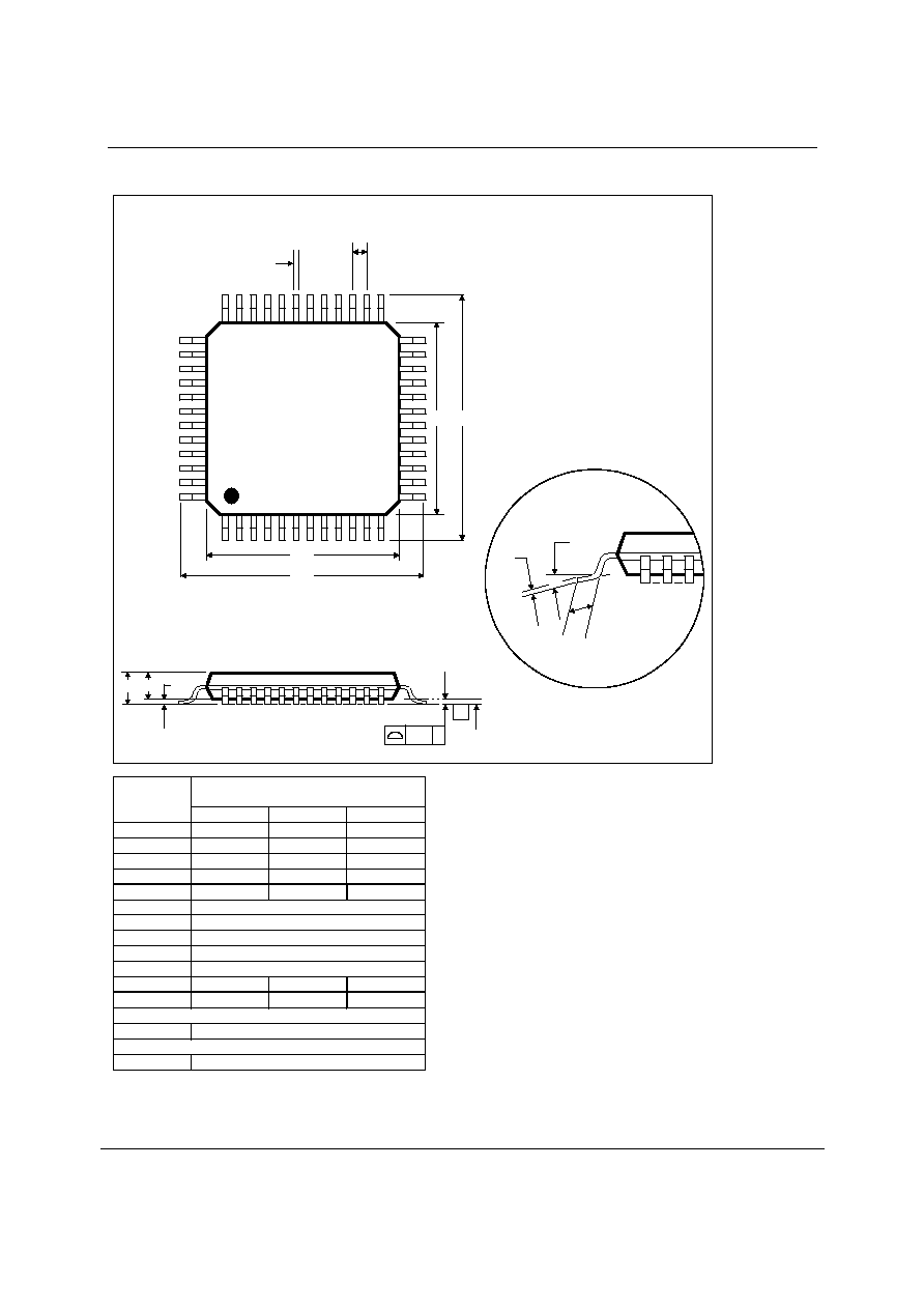
WM9705
Advance Information
AI Rev 3.6 October 2002
50
PACKAGE DIMENSIONS - TQFP
NOTES:
A. ALL LINEAR DIMENSIONS ARE IN MILLIMETERS.
B. THIS DRAWING IS SUBJECT TO CHANGE WITHOUT NOTICE.
C. BODY DIMENSIONS DO NOT INCLUDE MOLD FLASH OR PROTRUSION, NOT TO EXCEED 0.25MM.
D. MEETS JEDEC.95 MS-026, VARIATION = ABC. REFER TO THIS SPECIFICATION FOR FURTHER DETAILS.
DM004.C
FT: 48 PIN TQFP (7 x 7 x 1.0 mm)
Symbols
Dimensions
(mm)
MIN
NOM
MAX
A
-----
-----
1.20
A
1
0.05
-----
0.15
A
2
0.95
1.00
1.05
b
0.17
0.22
0.27
c
0.09
-----
0.20
D
9.00 BSC
D
1
7.00 BSC
E
9.00 BSC
E
1
7.00 BSC
e
0.50 BSC
L
0.45
0.60
0.75
4
0
o
3.5
o
7
o
Tolerances of Form and Position
ccc
0.08
REF:
JEDEC.95, MS-026
25
36
e
b
12
1
D1
D
E1
E
13
24
37
48
A
A2
A1
SEATING PLANE
ccc C
-C-
4
c
L
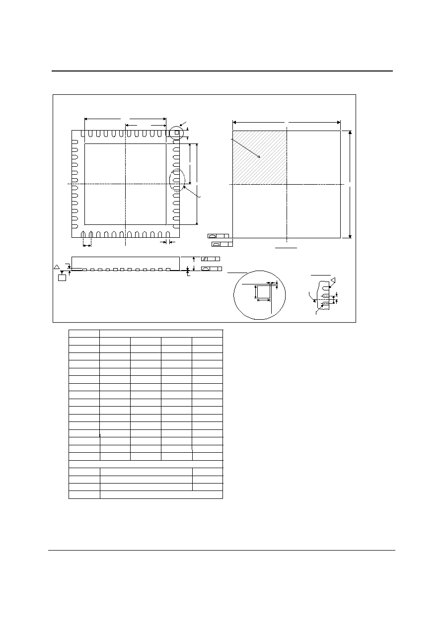
WM9705
Advance Information
AI Rev 3.6 October 2002
51
PACKAGE DIMENSIONS - QFN
DM029.A
FL: 48 PIN QFN PLASTIC PACKAGE 7
X
7
X
0.9 mm BODY, 0.50 mm LEAD PITCH
NOTES:
1. DIMENSION b APPLIED TO METALLIZED TERMINAL AND IS MEASURED BETWEEN 0.25 mm AND 0.30 mm FROM TERMINAL TIP.
2. ALL DIMENSIONS ARE IN MILLIMETRES
3. THIS DRAWING IS SUBJECT TO CHANGE WITHOUT NOTICE.
INDEX AREA
(D/2 X E/2)
TOP VIEW
C
aaa
2 X
SEE DETAIL B
E2
E2/2
b
D2
24
L
D2/2
C
aaa
2 X
DETAIL B
25
36
37
48
1
12
13
D
E
e
TERMI
NAL
TIP
R
DA
TUM
e
e/
2
1
Symbols
Dimensions (mm)
MIN
NOM
MAX
NOTE
A
b
D
D2
E
E2
e
L
R
0.80
0.90
1.00
0.30
0.23
0.18
7.00 BSC
5.25
5.15
5.00
7.00 BSC
0.5 BSC
5.15
5.25
5.00
0.30
0.4
0.50
b(min)/2
1
JEDEC, MO-220, VARIATION VKKD-2
Tolerances of Form and Position
SEE DETAIL A
A1
A3
0
0.02
0.05
0.20 REF
AA
BB
CC
DD
aaa
bbb
ccc
0.23
0.23
0.18
0.18
0.15
0.10
0.10
REF
AA
BB
DD
CC
DETAIL A
C
0.08
C
ccc
A
A1
C
(A3)
SEATING PLANE
1

WM9705
Advance Information
AI Rev 3.6 October 2002
52
IMPORTANT NOTICE
Wolfson Microelectronics Ltd (WM) reserve the right to make changes to their products or to discontinue any product or service
without notice, and advise customers to obtain the latest version of relevant information to verify, before placing orders, that
information being relied on is current. All products are sold subject to the WM terms and conditions of sale supplied at the time of
order acknowledgement, including those pertaining to warranty, patent infringement, and limitation of liability.
WM warrants performance of its products to the specifications applicable at the time of sale in accordance with WM's standard
warranty. Testing and other quality control techniques are utilised to the extent WM deems necessary to support this warranty.
Specific testing of all parameters of each device is not necessarily performed, except those mandated by government requirements.
In order to minimise risks associated with customer applications, adequate design and operating safeguards must be used by the
customer to minimise inherent or procedural hazards.
WM assumes no liability for applications assistance or customer product design. WM does not warrant or represent that any license,
either express or implied, is granted under any patent right, copyright, mask work right, or other intellectual property right of WM
covering or relating to any combination, machine, or process in which such products or services might be or are used. WM's
publication of information regarding any third party's products or services does not constitute WM's approval, license, warranty or
endorsement thereof.
Reproduction of information from the WM web site or datasheets is permissible only if reproduction is without alteration and is
accompanied by all associated warranties, conditions, limitations and notices. Representation or reproduction of this information with
alteration voids all warranties provided for an associated WM product or service, is an unfair and deceptive business practice, and
WM is not responsible nor liable for any such use.
Resale of W M's products or services with statements different from or beyond the parameters stated by WM for that product or
service voids all express and any implied warranties for the associated WM product or service, is an unfair and deceptive business
practice, and W M is not responsible nor liable for any such use.
ADDRESS:
Wolfson Microelectronics Ltd
20 Bernard Terrace
Edinburgh
EH8 9NX
United Kingdom
Tel :: +44 (0)131 272 7000
Fax :: +44 (0)131 272 7001
Email ::
sales@wolfsonmicro.com