GBU8A ≠ GBU8K 1 of 3 © 2002 Won-Top Electronics
GBU8A ≠ GBU8K
8.0A GLASS PASSIVATED BRIDGE RECTIFIER
Features
!
Glass Passivated Die Construction A
!
Low Forward Voltage Drop D
!
High Current Capability J
!
High Reliability C
!
High Surge Current Capability
!
Ideal for Printed Circuit Boards
+ ~ ~ -
E
G K
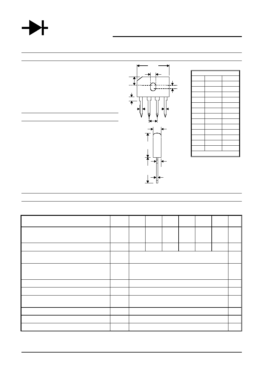
Mechanical Data
H
!
Case:
Molded
Plastic
!
Terminals: Plated Leads Solderable per M
MIL-STD-202, Method 208
!
Polarity: As Marked on Body
!
Weight: 4.0 grams (approx.) B
!
Mounting
Position:
Any
!
Marking: Type Number
L
N
P
Maximum Ratings and Electrical Characteristics
@T
A
=25∞C unless otherwise specified
Single Phase, half wave, 60Hz, resistive or inductive load.
For capacitive load, derate current by 20%.
Characteristic
Symbol
GBU8A
GBU8B
GBU8D
GBU8G
GBU8J
GBU8K
Unit
Peak Repetitive Reverse Voltage
Working Peak Reverse Voltage
DC Blocking Voltage
V
RRM
V
RWM
V
R
50
100
200
400
600
800
V
RMS Reverse Voltage
V
R(RMS)
35
70
140
280
420
560
V
Average Rectified Output Current @T
C
= 100∞C
@T
A
= 45∞C
I
O
8.0
6.0
A
Non-Repetitive Peak Forward Surge Current
8.3ms Single half sine-wave superimposed on
rated load (JEDEC Method)
I
FSM
200
A
I
2
t Rating for Fusing (t < 8.35ms)
I
2
t
166
A
2
s
Forward Voltage (per element) @I
F
= 8.0A
V
FM
1.0
V
Peak Reverse Current @T
A
= 25∞C
At Rated DC Blocking Voltage @T
C
= 100∞C
I
R
5.0
500
µA
Typical Thermal Resistance (per leg) (Note 1)
R
JA
18.0
K/W
Typical Thermal Resistance (per leg) (Note 2)
R
JC
3.0
K/W
Operating and Storage Temperature Range
T
j,
T
STG
-55 to +150
∞C
Note: 1. Thermal resistance junction to ambient, mounted on PCB at 9.5mm lead length with 12mm
2
copper pads.
2. Thermal resistance junction to case, mounted on 7.5 x 7.5 x 0.3cm thick AL plate.
W T E
PO W E R SEM IC O ND U C TO RS
GBU
Dim
Min
Max
A
21.80
22.30
B
18.30
18.80
C
7.40
7.90
D
3.50
4.10
E
1.52
2.03
G
2.16
2.54
H
4.83
5.33
J
1.65
2.16
K
1.65
2.03
L
0.76
1.02
M
3.30
3.56
N
17.50
18.00
P
0.46
0.56
All Dimensions in mm
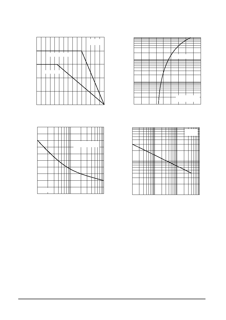
0.1
1.0
10
100
0.2
0.0
0.6
1.0
1.8
I
,
INST
ANT
A
NEOUS
FOR
W
A
RD
CURRENT
(
A)
F
V , INSTANTANEOUS FORWARD VOLTAGE (V)
Fig. 2 Typical Forward Characteristics
, per element
F
T = 25 C
j
∞
Pulse width = 300 s
µ
1.4
0
100
200
250
1
10
100
I
,
PEAK
FOR
W
ARD
SURGE
C
URRENT
(A)
FSM
NUMBER OF CYCLES AT 60 Hz
Fig. 3 Maximum Non-Repetitive Surge Current
Single Half-Sine Wave
(JEDEC Method)
T = 25 C
j
∞
0
2
4
6
8
10
0
50
100
150
I
,
A
V
G
FOR
W
A
RD
OUTPUT
CURRENT
(A)
(A
V)
T , TEMPERATURE ( C)
Fig. 1 Forward Current Derating Curve
∞
Resistive or
Inductive Load
Heatsink
PC Board
10
100
1000
0.1
1.0
10
100
C
,
JUNCTION
CAP
ACIT
ANCE
(pF)
j
V , REVERSE VOLTAGE (V)
Fig. 4 Typical Junction Capacitance
R
T = 25 C
j
∞
f = 1.0MHz
GBU8A ≠ GBU8K 2 of 3 © 2002 Won-Top Electronics

GBU8A ≠ GBU8K
3 of 3 © 2002 Won-Top Electronics
ORDERING INFORMATION
Product No.
Package Type
Shipping Quantity
GBU8A
SIL Bridge
25 Units/Tube
GBU8B
SIL Bridge
25 Units/Tube
GBU8D
SIL Bridge
25 Units/Tube
GBU8G
SIL Bridge
25 Units/Tube
GBU8J
SIL Bridge
25 Units/Tube
GBU8K
SIL Bridge
25 Units/Tube
Shipping quantity given is for minimum packing quantity only. For minimum order
quantity, please consult the Sales Department.
Won-Top Electronics Co., Ltd (WTE) has checked all information carefully and believes it to be correct and accurate. However, WTE cannot assume any
responsibility for inaccuracies. Furthermore, this information does not give the purchaser of semiconductor devices any license under patent rights to
manufacturer. WTE reserves the right to change any or all information herein without further notice.
WARNING: DO NOT USE IN LIFE SUPPORT EQUIPMENT. WTE power semiconductor products are not authorized for use as critical components in life
support devices or systems without the express written approval.
We power your everyday.
Won-Top Electronics Co., Ltd.
No. 44 Yu Kang North 3rd Road, Chine Chen Dist., Kaohsiung, Taiwan
Phone: 886-7-822-5408 or 886-7-822-5410
Fax: 886-7-822-5417
Email: sales@wontop.com
Internet: http://www.wontop.com