XECOM
(1)
XE5620SM
XE5620SM
February 2003
Compact Global Modem Board
Description
Xecom's XE5620SM is a complete modem on a compact
PCB (daughter board). Xecom includes transferable
FCC Part 68 Registration to the user of the XE5620SM.
This allows the embedded system designer to easily add
modem communications to his process control, remote
monitoring, point-of-sale, or remote diagnostic system
without additional FCC testing.
Xecom's XE5620SM has a twenty percent smaller
footprint than other modem daughter board products.
This reduced footprint saves board space and allows
the design engineer greater flexibility in placement of the
modem within the host system.
A variation of the XE5620SM, the XE5620SM-F,
incorporates Flash memory onto the daughter board.
The presence of Flash memory allows future updating of
the modem code when features are added.
Features
* Small Size: 2.175" by 1.00" by 0.3"
* Data transfer at rates from 300 bps to 56 kbps using
V.90, V.34bis, V.34, V.32bis, V.32, V.22bis, V.22, V.23, V.21,
Bell 212A, and Bell 103 Protocols
* Modem Control and Configuration via industry
standard AT Commands.
* Supports V.42 error correction and V.42bis data
compression.
* Nonvolatile memory stores modem configuration and
permits stored number dialing.
* Incorporates Fax send and receive capabilities
controlled by Class 1 Fax commands.
* Complete integrated DAA.
* User Transferrable FCC Part 68 Registration
* Complies with telephone networks around the world.
* UL60950 Recognition
* Low Power operation, 3.3 Volts, 300 milliwatts;
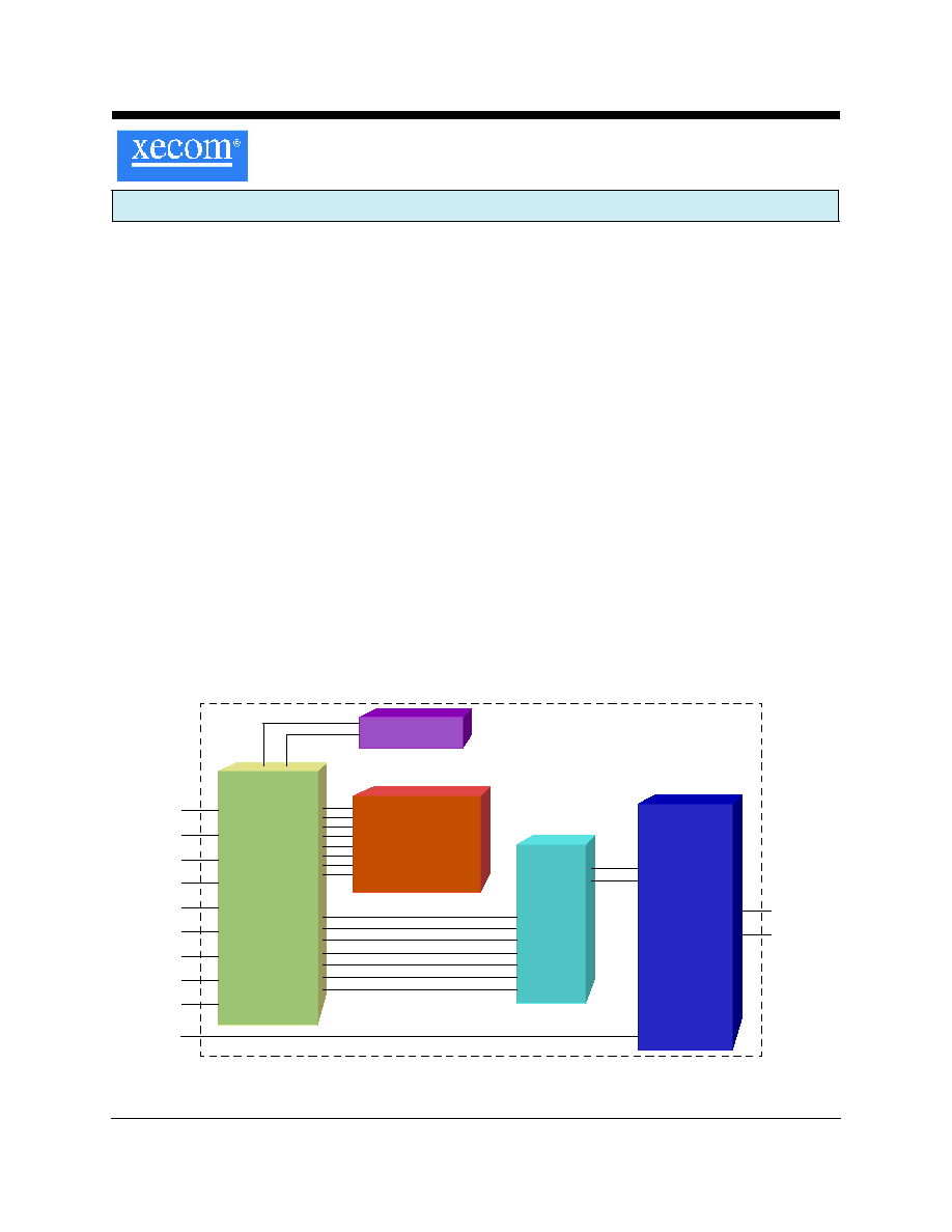
XE5620SM/XE5620SM-F BLOCK DIAGRAM
Modem
Controller
Tip
Ring
Reset
/TXD
/RXD
/RTS
/DSR
/DCD
/CTS
/DTR
/RI
SPKR
NVRAM
Analog
Front
End
Global
Telephone
Line
Interface
(DAA)
ROM or Flash
(XE5620SM-F)
Preliminary

XECOM
(2)
XE5620SM
XE5620SM Mechanical Specifications
Inches
Millimeters
Dimension
Min
Typ
Max
Min
Typ
Max
a
2.170
2.175
2.180
55.12
55.24
55.37
b
0.995
1.000
1.005
25.27
25.40
25.53
c
0.890
0.900
0.910
22.61
22.86
23.11
d
0.110
0.120
0.130
2.79
3.05
3.30
e
0.090
0.100
0.110
2.29
2.54
2.79
f
0.240
0.250
0.260
6.10
6.35
6.60
g
0.059
0.062
0.065
1.50
1.57
1.65
h
0.790
0.800
0.810
20.07
20.32
20.83
j
0.090
0.100
0.110
2.29
2.54
2.79
k
0.137 0.1375
0.138
3.48
3.49
3.51
l
1.230
1.240
1.250
31.24
31.50
31.75
m
1.490
1.500
1.510
37.85
38.10
38.35
n
0.290
0.300
0.310
7.37
7.62
7.87
(Top View)
a
b
c
d
f
e
g
h
k
l
m
k
j
j
k
j
n
Note: All pins are .025" square
XECOM
(3)
XE5620SM
XE5620SM Pin Configuration
Pin Descriptions
PIN NAME
DESCRIPTION
1
Tip
The Ring and Tip signals connect the modem to the telephone line. FCC Part 68 Rules require a
1500 volt isolation barrier between the telephone line and all other circuits. This isolation must
be preserved throughout the system.
The telephone company places a DC "Battery" voltage across Tip and Ring on public switched
telephone lines. The XE5620SM operates regardless of the polarity of this "Battery" voltage.
The "Battery" voltage drives up to 100 milliampere of DC loop current.
UL60950 requires minimum creepage and clearances distances between the Tip and Ring traces
and all other circuits. Clearance is the shortest distance between conductive circuits; creepage
is the distance between conductive points along the surface
2
Ring
The Ring and Tip signals connect the modem to the telephone line. FCC Part 68 Rules require a
1500 volt isolation barrier between the telephone line and all other circuits. This isolation must
be preserved throughout the system.
The telephone company places a DC "Battery" voltage across Tip and Ring on public switched
telephone lines. The XE5620SM operates regardless of the polarity of this "Battery" voltage.
The "Battery" voltage drives up to 100 milliampere of DC loop current.
Top View
1
2
3
4
5
6
1 5
1 4
1 3
1 2
1 1
1 0
9
8
7
Tip
Ring
EXM
/Reset
SPKR
Gnd
VCC
/DCD
/CTS
/DSR
/RTS
/RXD
/TXD
/DTR
/RI

XECOM
(4)
XE5620SM
UL60950 requires minimum creepage and clearances distances between the Tip and Ring traces
and all other circuits. Clearance is the shortest distance between conductive circuits; creepage
is the distance between conductive points along the surface.
3
EXM
EXM will be high when Flash memory is used, XE5620SM-F. Do not attach any signal to this pin.
4
RESET
RESET is an active low input which initiates a modem hardware reset. RESET must be active for
a minimum of 100 milliseconds for a proper modem reset sequence. No external reset is required;
if none is used the RESET signal should be left open.
5
SPKR
SPKR allows connection of a speaker to monitor modem operations. SPKR cannot directly drive
a speaker; an amplifier with a minimum input impedance of 300 ohms is required. The signal on
SPKR is controlled by the ATL and ATM commands.
6
Ground
Ground provides the reference voltage for all host interface signals.
7
/RI
The /RI signal reports on the presence of an incoming ring signal. When a ring occurs across
Tip and Ring, the /RI output goes low and toggles with the cadence of the ring signal..
8
/DTR
/DTR is an active low input to the modem. An active /DTR signals the terminal is available for
communications. The AT&D command determines how the modem interprets activity on /DTR.
9
/TXD
/TXD provides the path for transmitted data and modem commands to be passed from the host
controller to the modem.
10
/RXD
/RXD provides the path for received data and modem responses to be sent from the modem to
the host controller.
11
/RTS
/RTS is an active low input to the modem. When hardware flow control is set, ab active /RTS
indicates to the modem that the host has data to send.
12
/DSR
/DSR is an active low output from the modem. An active /DSR indicates the modem link is
established. The AT&S command controls when the XE5620SM asserts /DSR.
13
/CTS
/CTS is an active low output from the modem. When hardware flow control is set, the modem
asserts /CTS to indicate that it can accept data from the terminal equipment on /TXD.
14
/DCD
/DCD is an active low output from the modem. An active /DCD indicates the presence of a valid
carrier signal. The AT&C command controls when the XE5620SM asserts /DCD.
15
VCC
VCC provides 3.3 volt power to the modem.
XE5620SM Pin Descriptions (continued)
PIN NAME
DESCRIPTION
XECOM
(5)
XE5620SM
XE5620SM Electrical Specifications
VCC
3.13
3.3
3.47
Volts
ICC
8 5
9 0
1 0 0
ma
On Line
ICC
2 5
ma
On-Hook
Ring Voltage Detected
2 6
1 5 0
VRMS
Type B Ringer
Ring Frequency Detected
15.3
6 8
Hz
Type B Ringer
Telephone Loop Current
1 0
4 0
1 0 0
ma
Line Impedance
6 0 0
Ohms
Data Transmit level
-12.0
-9.0
dBm
DTMF Transmit Level
-2.5
0
dBm
Avg over 3 second interval
Vo h
2.4
Volts
Vol
0.4
Volts
Vih
2.0
VCC+0.3
Volts
Vil
-0.3
0.8
Volts
Parameter
Min
Typ
Max
Units
Comments
XE5620SM ABSOLUTE MAXIMUM RATINGS
Storage Temperature
-25
O
C to +85
O
C
1
Maximum Operating Temperature Range
0
O
C to +70
O
C
Maximum Time Above Eutectic (183
O
C)
90 seconds
Preheat Dwell Time
120 to 180 seconds
1
The XE5620SM can be ordered with an Operating Temperature of -40
O
C to +85
O
C at extra cost. Order
XE5620SM-ITR or to specify Industrial Temperature Range (ITR).