 | –≠–ª–µ–∫—Ç—Ä–æ–Ω–Ω—ã–π –∫–æ–º–ø–æ–Ω–µ–Ω—Ç: X1240S8 | –°–∫–∞—á–∞—Ç—å:  PDF PDF  ZIP ZIP |
Preliminary Information
©
Xicor, Inc. 1994, 1995, 1996, 1997, 1998, 1999 Patents Pending
9900-3003.5 12/6/99 CM
1
Characteristics subject to change without notice
16K
2-Wire RTC
Real Time Clock/Calendar with EEPROM
FEATURES
∑ 2-Wire Interface interoperable with I
2
C.
--400kHz data transfer rate
∑ Secondary Power Supply Input with internal
switch-over circuitry.
∑ Year 2000 Compliant
∑ 2K bytes of EEPROM
--64 Byte Page Write Mode
--3 bit Block Lock
∑ Low Power CMOS
--<1
µ
A Operating Current
--<3mA Active Current during Program
--<400
µ
A Active Current during Data Read
∑ Single Byte Write Capability
∑ Typical Nonvolatile Write Cycle Time: 5ms
∑ High Reliability
--1,000,000 Endurance Cycles
--Guaranteed Data Retention: 100 Years
∑ Small Package Options
--8-Lead SOIC Package, 8L TSSOP Package
DESCRIPTION
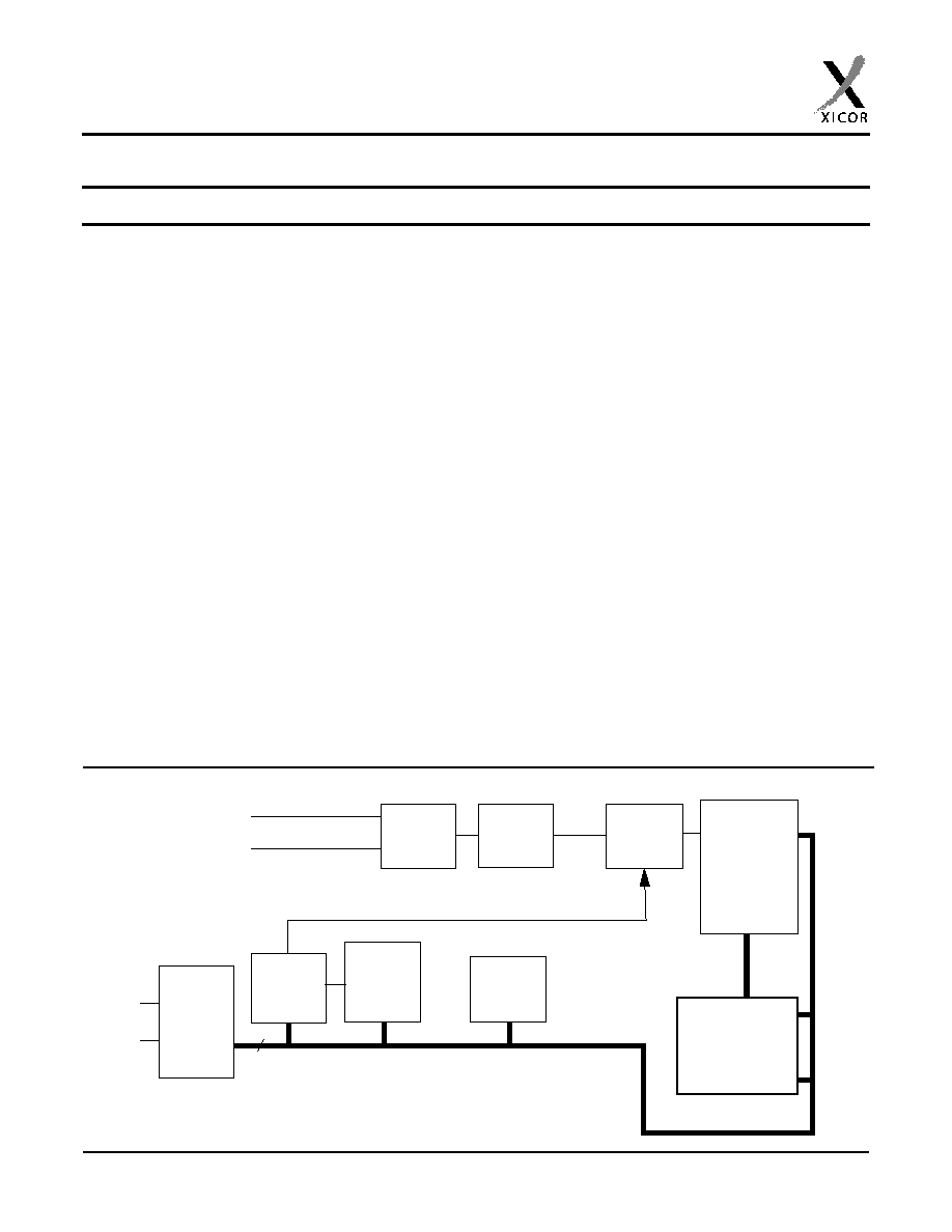
The X1240 is a Real Time Clock with clock/calendar
circuits. The dual port clock register allows the clock to
operate, without loss of accuracy, even during read and
write operations.
The clock/calendar provides functionality that is con-
trollable and readable through a set of registers. The
clock, using a low cost 32.768kHz crystal input, accu-
rately tracks the time in seconds, minutes, hours, date,
day, month and years. It has leap year correction,
automatic adjustment for the year 2000 and months
with less than 31 days.
The device offers a backup power input pin. This
Vback pin allows the device to be backed up by a non-
rechargeable battery. The RTC is fully operational
from 1.8 to 5.5 volts.
The X1240 provides a 2K byte EEPROM array, giving
a safe, secure memory for critical user and configura-
tion data. This memory is unaffected by complete fail-
ure of the main and backup supplies.
BLOCK DIAGRAM
X1
X2
Oscillator
Frequency
Timer
Logic
Divider
Calendar
8
32.768kHz
Control
Registers
1Hz
Time
Keeping
Registers
Control
Decode
Logic
(EEPROM)
(SRAM)
SCL
SDA
Serial
Interface
Decoder
16K
EEPROM
Array
Register
Status
(SRAM)
X1240
X1240
2
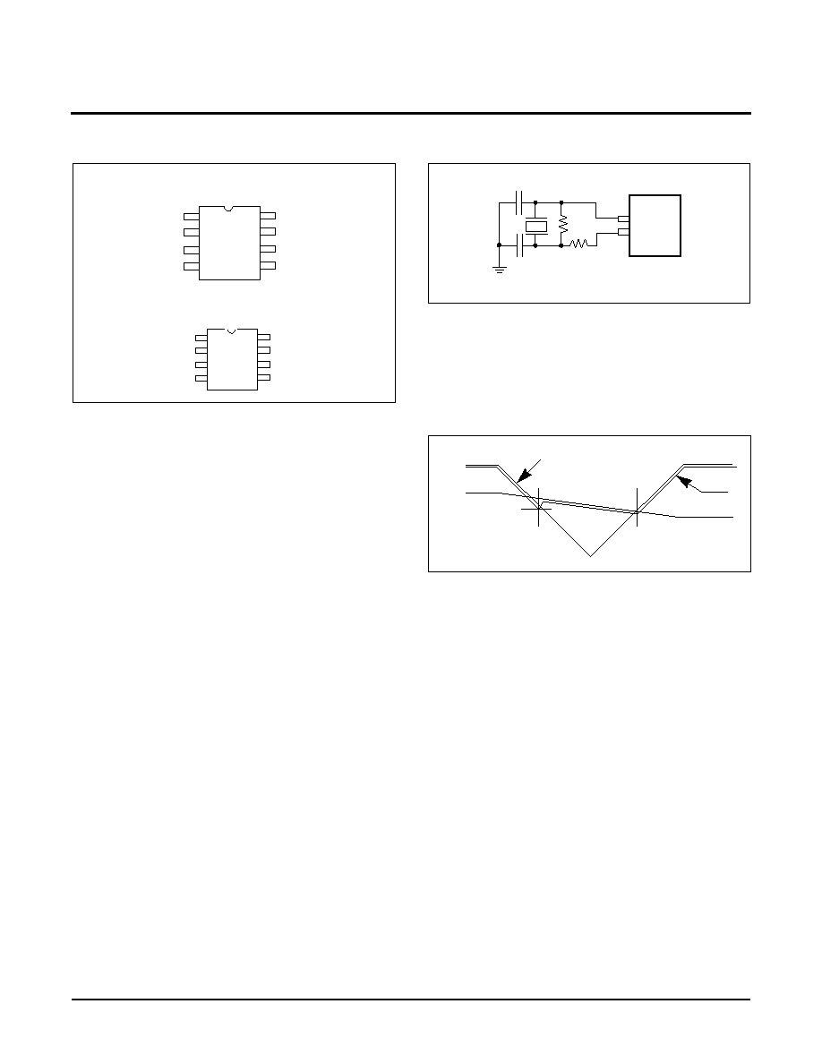
PIN CONFIGURATION
PIN DESCRIPTIONS
Serial Clock (SCL)
The SCL input is used to clock all data into and out of
the device. The input buffer on this pin is always active
(not gated).
Serial Data (SDA)
SDA is a bidirectional pin used to transfer data into
and out of the device. It has an open drain output and
may be wire ORed with other open drain or open col-
lector outputs. The input buffer is always active (not
gated).
An open drain output requires the use of a pull-up
resistor. The output circuitry controls the fall time of
the output signal with the use of a slope controlled
pull-down. The circuit is designed for 400kHz 2-wire
interface speeds.
V
BACK
This input provides a backup supply voltage to the
device. V
BACK
supplies power to the device in the
event the V
CC
supply fails.
X1, X2
The X1 and X2 pins are the input and output, respec-
tively, of an inverting amplifier that can be configured
for use as an on-chip oscillator. A 32.768kHz quartz
crystal is used. Recommeded crystals are Sieko VT-200
or Epson C-002RX. The crystal supplies a timebase
for a clock/oscillator. The internal clock can be driven
by an external signal on X1, with X2 left unconnected.
Figure 1. Recommended Crystal connection
POWER CONTROL OPERATION
The Power control circuit accepts a V
CC
and a V
BACK
input. The power control circuit will switch to V
BACK
when V
CC
< V
BACK
- 0.2V. It will switch back to V
CC
when V
CC
exceeds V
BACK
.
Figure 2. Power Control
REAL TIME CLOCK OPERATION
The Real Time Clock (RTC) uses an external, 32.768KHz
quartz crystal to maintain an accurate internal repre-
sentation of the year, month, day, date, hour, minute,
and seconds. The RTC has leap-year correction and a
century byte. The clock will also correct for months hav-
ing fewer than 31 days and will have a bit that controls
24 hour or AM/PM format. When the X1240 powers up
after the loss of both V
CC
and V
BACK
, the clock will not
increment until at least one byte is written to the clock
register.
Reading the Real Time Clock
The RTC is read by initiating a Read command and
specifying the address corresponding to the register of
the Real Time Clock. The RTC Registers can then be
read in a Sequential Read Mode. Since the clock runs
continuously and a read takes a finite amount of time,
there is the possibility that the clock could change dur-
ing the course of a read operation. In this device, the
time is latched by the read command (falling edge of
X1240
X1
X2
V
Back
V
CC
NC
SCL
SDA
V
SS
1
2
3
4
7
8
6
5
8 pin TSSOP
X1240
X1
X2
V
Back
V
CC
NC
SCL
SDA
V
SS
1
2
3
4
7
8
6
5
8 pin SOIC
X1
X2
43pF
18pF
220K
10M
V
BACK
V
CC
= V
BACK
-0.2V
Internal
Voltage
V
CC

X1240
3
the clock on the ACK bit prior to RTC data output) into
a separate latch to avoid time changes during the read
operation. The clock continues to run.
Writing to the Real Time Clock
The time and date may be set by writing to the RTC
registers. To avoid changing the current time by an
uncompleted write operation, the current time value is
loaded into a seperate buffer at the falling edge of the
clock on the ACK bit before the RTC data input bytes,
the clock continues to run. The new serial input data
replaces the values in the buffer. This new RTC value
is loaded back into the RTC Register by a stop bit at
the end of a valid write sequence. An invalid write
operation aborts the time update procedure and the
contents of the buffer are discarded. After a valid write
operation the RTC will reflect the newly loaded data
beginning with the first "one second" clock cycle after
the stop bit. The RTC continues to update the time
while an RTC register write is in progress and the RTC
continues to run during any nonvolatile write sequences.
A single byte may be written to the RTC without affect-
ing the other bytes.
CLOCK/CONTROL REGISTERS (CCR)
The Control/Clock Registers are located in an area
logically separated from the array and are only acces-
sible following a slave byte of "1101111x" and reads or
writes to addresses [0000h:003Fh].
CCR access
The contents of the CCR can be modified by performing
a byte or a page write operation directly to any address in
the CCR. Prior to writing to the CCR (except the status
register), however, the WEL and RWEL bits must be
set using a two step process (See section "Writing to
the Clock/Control Registers.")
The CCR is divided into 3 sections. These are:
1. Control (2 bytes)
2. Real Time Clock (8 bytes)
3. Status (1 byte)
Sections 1) and 2) are nonvolatile and Section 3) is
volatile. Each register is read and written through buff-
ers. The non-volatile portion (or the counter portion of
the RTC) is updated only if RWEL is set and only after
a valid write operation and stop bit. A sequential read or
page write operation provides access to the contents
of only one section of the CCR per operation. Access
to another section requires a new operation. Contin-
ued reads or writes, once reaching the end of a sec-
tion, will wrap around to the start of the section. A read
or page write can begin at any address in the CCR.
Section 3) is a volatile register. It is not necessary to set
the RWEL bit prior to writing the status register. Section 3)
supports a single byte read or write only. Continued reads
or writes from this section terminates the operation.
The state of the CCR can be read by performing a ran-
dom read at any address in the CCR at any time. This
returns the contents of that register location. Additional
registers are read by performing a sequential read.
The read instruction latches all Clock registers into a
buffer, so an update of the clock does not change the
time being read. A sequential read of the CCR will not
result in the output of data from the memory array. At
the end of a read, the master supplies a stop condition
to end the operation and free the bus. After a read of
the CCR, the address remains at the previous address
+1 so the user can execute a current address read of
the CCR and continue reading the next Register.
X1240
4
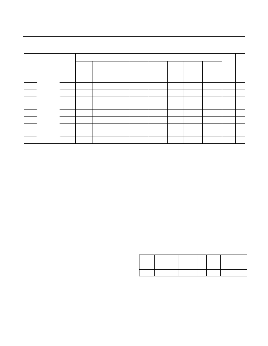
Table 1. Clock/Control Memory Map
Addr.
Type
Reg
Name
Bit
Range
Factroy
Settings
7
6
5
4
3
2
1
0
(optional)
003F
Status
SR
BAT
0
0
0
0
RWEL
WEL
RTCF
0037
RTC
(SRAM)
Y2K
0
0
Y2K21
Y2K20
Y2K13
0
0
Y2K10
19/20
0036
DW
0
0
0
0
0
DY2
DY1
DY0
0-6
0035
YR
Y23
Y22
Y21
Y20
Y13
Y12
Y11
Y10
0-99
0034
MO
0
0
0
G20
G13
G12
G11
G10
1-12
0033
DT
0
0
D21
D20
D13
D12
D11
D10
1-31
0032
HR
MIL
0
H21
H20
H13
H12
H11
H10
0-23
0031
MN
0
M22
M21
M20
M13
M12
M11
M10
0-59
0030
SC
0
S22
S21
S20
S13
S12
S11
S10
0-59
0011
Control
(E2PROM)
INT
0
0
0
0
0
0
0
0
00h
0010
BL
BP2
BP1
BP0
0
0
0
0
0
00h
REAL TIME CLOCK REGISTERS
Year 2000 (Y2K)
The X1240 has a century byte that "rolls over" from 19
to 20 when the years byte changes from 99 to 00. The
Y2K byte can contain only the values of 19 or 20.
Day of the Week Register (DW)
This register provides a Day of the Week status and
uses three bits DY2 to DY0 to represent the seven
days of the week. The counter advances in the cycle
0-1-2-3-4-5-6-0-1-2-... The assignment of a numerical
value to a specific day of the week is arbitrary and may
be decided by the system software designer. The
Clock Default values define 0=Sunday.
Clock/Calendar Registers (YR, MO, DT, HR, MN, SC)
These registers depict BCD representations of the
time. As such, SC (Seconds) and MN (Minutes) range
from 00 to 59, HR (Hour) is 1 to 12 with an AM or PM
indicator (H21 bit) or 0 to 23 (with MIL=1), DT (Date) is
1 to 31, MO (Month) is 1 to 12, YR (year) is 0 to 99.
24 Hour Time
If the MIL bit of the HR register is 1, the RTC will use a
24-hour format. If the MIL bit is 0, the RTC will use 12-
hour format and bit H21 will function as an AM/PM
indicator with a `1' representing PM. The clock defaults
to Standard Time with H21=0.
Leap Years
Leap years add the day February 29 and are defined
as those years that are divisible by 4. Years divisible
by 100 are not leap years, unless they are also divisi-
ble by 400. This means that the year 2000 is a leap
year, the year 2100 is not. The X1240 does not correct
for the leap year in the year 2100.
STATUS REGISTER (SR)
The Status Register is located in the RTC area at
address 003FH. This is a volatile register only and is
used to control the WEL and RWEL write enable
latches, and read a Low Voltage Sense bit. This regis-
ter is logically seperated from both the array and the
Clock/Control Registers (CCR).
Table 2. Status Register (SR)
BAT: Battery Supply--Volatile
This bit set to "1" indicates that the device is operating
from V
BACK
, not V
CC
. It is a read only bit and is set/
reset by hardware.
Addr
7
6
5
4
3
2
1
0
003Fh
BAT
0
0
0
0
RWEL
WEL
RTCF
Default
0
0
0
0
0
0
0
0
X1240
5
RWEL: Register Write Enable Latch--Volatile
This bit is a volatile latch that powers up in the LOW
(disabled) state. The RWEL bit must be set to "1" prior
to any writes to the Clock/Control Registers. Writes to
RWEL bit do not cause a nonvolatile write cycle, so the
device is ready for the next operation immediately after
the stop condition. A write to the CCR requires both the
RWEL and WEL bits to be set in a specific sequence.
WEL: Write Enable Latch--Volatile
The WEL bit controls the access to the CCR and mem-
ory array during a write operation. This bit is a volatile
latch that powers up in the LOW (disabled) state. While
the WEL bit is LOW, writes to the CCR or any array
address will be ignored (no acknowledge will be issued
after the Data Byte). The WEL bit is set by writing a "1"
to the WEL bit and zeroes to the other bits of the Status
Register. Once set, WEL remains set until either reset
to 0 (by writing a "0" to the WEL bit and zeroes to the
other bits of the Status Register) or until the part pow-
ers up again. Writes to WEL bit do not cause a non-vol-
atile write cycle, so the device is ready for the next
operation immediately after the stop condition.
RTCF: Real Time Clock Fail Bit--Volatile
This bit is set to a `1' after a total power failure. This is a
read only bit that is set by hardware when the device
powers up after having lost all power to the device. The
bit is set regardless of whether V
CC
or V
BACK
is applied
first. The loss of one or the other supplies does not
result in setting the RTCF bit. The first valid write to the
RTC (writing one byte is sufficient) resets the RTCF bit
to `0'.
Unused Bits:
These devices do not use bits 3 through 6, but must
have a zero in these bit positions. The Data Byte output
during a SR read will contain zeros in these bit locations.
CONTROL REGISTERS
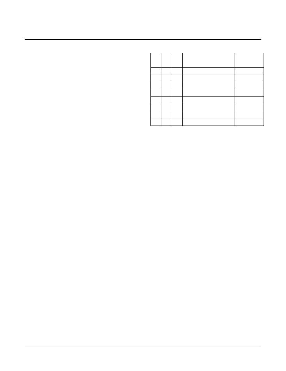
Block Protect Bits - BP2, BP1, BP0 - (Nonvolatile)
The Block Protect Bits, BP2, BP1 and BP0, determine
which blocks of the array are write protected. A write to
a protected block of memory is ignored. The block pro-
tect bits will prevent write operations to one of eight
segments of the array. The partitions are described in
Table 3.
Table 3. Block Protect Bits
WRITING TO THE CLOCK/CONTROL REGISTERS
Changing any of the nonvolatile bits of the clock/control
register requires the following steps:
--Write a 02H to the Status Register to set the Write
Enable Latch (WEL). This is a volatile operation, so
there is no delay after the write. (Operation pre-
ceeded by a start and ended with a stop).
--Write a 06H to the Status Register to set both the
Register Write Enable Latch (RWEL) and the WEL
bit. This is also a volatile cycle. The zeros in the data
byte are required. (Operation preceeded by a start
and ended with a stop).
--Write one to 8 bytes to the Clock/Control Registers
with the desired clock, or control data. This sequence
starts with a start bit, requires a slave byte of
"11011110" and an address within the CCR and is
terminated by a stop bit. A write to the CCR changes
EEPROM values so these initiate a nonvolatile write
cycle and will take up to 10ms to complete. Writes to
undefined areas have no effect. The RWEL bit is
reset by the completion of a nonvolatile write write
cycle, so the sequence must be repeated to again ini-
tiate another change to the CCR contents. If the
sequence is not completed for any reason (by send-
ing an incorrect number of bits or sending a start
instead of a stop, for example) the RWEL bit is not
reset and the device remains in an active mode.
--Writing all zeros to the status register resets both the
WEL and RWEL bits.
--A read operation occurring between any of the previ-
ous operations will not interrupt the register write
operation.
--The RWEL and WEL bits can be reset by writing a 0
to the Status Register.
BP2
BP1
BP0
Protected Addresses
X1240
Array Lock
0
0
0
None
None
0
0
1
600h - 7FFh
Upper 1/4
0
1
0
400h - 7FFh
Upper 1/2
0
1
1
000h - 7FFh
Full Array
1
0
0
000h - 03Fh
First Page
1
0
1
000h - 07Fh
First 2 pgs
1
1
0
000h - 0FFh
First 4 pgs
1
1
1
000h - 1FFh
First 8 Pgs