Document Outline
- Table of Contents
- Product Selection
- Data Sheet Alpha
- Ap Note Alpha
X20C05
1
High Speed AUTOSTORETM NOVRAM
4K
X20C05
512 x 8
FEATURES
∑
Fast Access Time: 35ns, 45ns, 55ns
∑
High Reliability
--Endurance: 1,000,000 Nonvolatile Store
Operations
--Retention: 100 Years Minimum
∑
Power-on Recall
--E
2
PROM Data Automatically Recalled Into
SRAM Upon Power-up
∑
AUTOSTORETM NOVRAM
--User Enabled Option
--Automatically Stores SRAM Data Into the
E
2
PROM Array When V
CC
Low Threshold is
Detected
--Open Drain AUTOSTORE Status Output Pin
∑
Software Data Protection
--Locks Out Inadvertent Store Operations
∑
Low Power CMOS
--Standby: 250
µ
A
∑
Infinite E
2
PROM Array Recall, and RAM Read
and Write Cycles
∑
Upward compatible with X20C16 (16K)
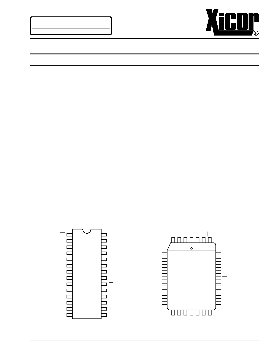
PIN CONFIGURATION
PLASTIC
CERDIP
3827 FHD F02
NE
NC
7
A6
A5
A4
A3
A2
A1
A0
I/O0
I/O1
I/O2
V
1
VCC
WE
AS
A8
NC
NC
OE
NC
CE
I/O7
I/O6
I/O5
I/O4
I/O3
X20C05
2
3
4
5
6
7
8
9
10
11
12
13
14
28
27
26
25
24
23
22
21
20
19
18
17
16
15
LCC
PLCC
A
7
A6
A5
A4
A3
A2
A1
A0
NC
I/O0
A8
NC
NC
NC
OE
NC
CE
I/O7
I/O6
NC
NE
NC
V
CC
WE
AS
I/O
1
I/O
2
V
SS
NC
I/O
3
I/O
4
I/O
5
4
3
2
1 32 31 30
14 15 16 17 18 19 20
5
6
7
8
9
10
11
12
13
29
28
27
26
25
24
23
22
21
X20C05
(TOP VIEW)
3827 FHD F03
DESCRIPTION
The Xicor X20C05 is a 512 x 8 NOVRAM featuring a
high-speed static RAM overlaid bit-for-bit with a non-
volatile electrically erasable PROM (E
2
PROM). The
X20C05 is fabricated with advanced CMOS floating
gate technology to achieve high speed with low power
and wide power-supply margin. The X20C05 features
the JEDEC approved pinout for byte-wide memories,
compatible with industry standard RAMs, ROMs,
EPROMs, and E
2
PROMs.
The NOVRAM design allows data to be easily trans-
ferred from RAM to E
2
PROM (store) and E
2
PROM to
RAM (recall). The store operation is completed in 5ms or
less and the recall operation is completed in 5
µ
s or less.
Xicor NOVRAMS are designed for unlimited write
operations to RAM, either from the host or recalls from
E
2
PROM, and a minimum 1,000,000 store operations to
the E
2
PROM. Data retention is specified to be greater
than 100 years.
AUTOSTORETM NOVRAM is a trademark of Xicor, Inc.
©Xicor, Inc. 1991 - 1997 Patents Pending
Characteristics subject to change without notice
3827-2.7 7/31/97 T4/C0/D0 SH
A
PPLICATION
N
OTE
A V A I L A B L E
AN56
X20C05
2
PIN DESCRIPTIONS
Addresses (A
0
≠A
8
)
The Address inputs select an 8-bit memory location
during a read or write operation.
Chip Enable (
CE
)
The Chip Enable input must be LOW to enable all read/
write operations. When
CE
is HIGH, power consumption
is reduced.
Output Enable (
OE
)
The Output Enable input controls the data output buffers
and is used to initiate read and recall operations. Output
Enable LOW disables a store operation regardless of
the state of
CE
,
WE,
or
NE
.
Data In/Data Out (I/O
0
≠I/O
7
)
Data is written to or read from the X20C05 through the
I/O pins. The I/O pins are placed in the high impedance
state when either
CE
or
OE
is HIGH or when
NE
is LOW.
Write Enable (
WE
)
The Write Enable input controls the writing of data to the
RAM.
Nonvolatile Enable (
NE
)
The Nonvolatile Enable input controls the recall function
to the E
2
PROM array.
AUTOSTORE Output (
AS
)
AS
is an open drain output which, when asserted indi-
cates V
CC
has fallen below the AUTOSTORE threshold
(V
ASTH
).
AS
may be wire-ORed with multiple open drain
outputs and used as an interrupt input to a microcontroller.
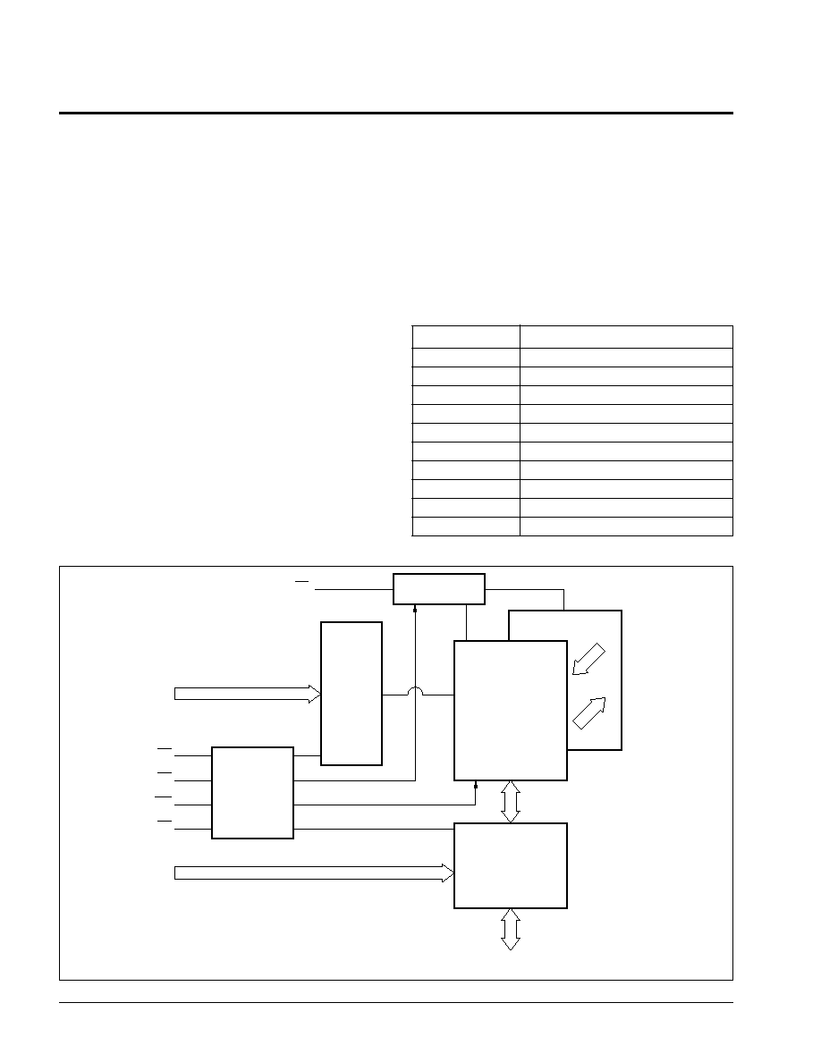
VCC SENSE
ROW
SELECT
CONTROL
LOGIC
COLUMN
SELECT
&
I/OS
EEPROM ARRAY
HIGH SPEED
512 x 8
SRAM
ARRAY
CE
OE
WE
NE
A3≠A6
I/O0≠I/O7
AS
A0≠A2
A7≠A8
RECALL
ST
ORE
3827 FHD F01
PIN NAMES
Symbol
Description
A
0
≠A
8
Address Inputs
I/O
0
≠I/O
7
Data Input/Output
WE
Write Enable
CE
Chip Enable
OE
Output Enable
NE
Nonvolatile Enable
AS
AUTOSTORE Output
V
CC
+5V
V
SS
Ground
NC
No Connect
3827 PGM T01
FUNCTIONAL DIAGRAM
X20C05
3
DEVICE OPERATION
The
CE
,
OE
,
WE
and
NE
inputs control the X20C05
operation. The X20C05 byte-wide NOVRAM uses a
2-line control architecture to eliminate bus contention in
a system environment. The I/O bus will be in a high
impedance state when either
OE
or
CE
is HIGH, or
when
NE
is LOW.
RAM Operations
RAM read and write operations are performed as they
would be with any static RAM. A read operation requires
CE
and
OE
to be LOW with
WE
and
NE
HIGH. A write
operation requires
CE
and
WE
to be LOW with
NE
HIGH. There is no limit to the number of read or write
operations performed to the RAM portion of the X20C05.
MEMORY TRANSFER OPERATIONS
There are two memory transfer operations: a recall
operation whereby the data stored in the E
2
PROM array
is transferred to the RAM array; and a store operation
which causes the entire contents of the RAM array to be
stored in the E
2
PROM array.
Recall operations are performed automatically upon
power-up and under host system control when
NE
,
OE
and
CE
are LOW and
WE
is HIGH. The recall operation
takes a maximum of 5
µ
s.
There are two methods of initiating a store operation.
The first is the software store command. This command
takes the place of the hardware store employed on the
X20C04. This command is issued by entering into the
special command mode:
NE
,
CE,
and
WE
strobe LOW
while at the same time a specific address and data
combination is sent to the device. This is a three step
operation: the first address/data combination is
155[H]/AA[H]; the second combination is 0AA[H]/55[H];
and the final command combination is 155[H]/33[H].
This sequence of pseudo write operations will immedi-
ately initiate a store operation. Refer to the software
command timing diagrams for details on set and hold
times for the various signals.
The second method of storing data is through the
AUTOSTORE command. When enabled, data is auto-
matically stored from the RAM into the E
2
PROM array
whenever V
CC
falls below the preset AUTOSTORE
threshold. This feature is enabled by performing the first
two steps for the software store with the command
combination being 155[H]/CC[H].
The AUTOSTORE feature is disabled by issuing the
three step command sequence with the command com-
bination being 155[H]/CD[H]. The AUTOSTORE feature
will also be reset if V
CC
falls below the power-up reset
threshold (approximately 3.5V) and is then raised back
into the operating range.
DATA PROTECTION
The X20C05 supports two methods of protecting the
nonvolatile data.
--If after power-up the AUTOSTORE feature is not
enabled, no AUTOSTORE can occur.
--If after power-up no RAM write operations have oc-
curred no store operation can be initiated. The software
store and AUTOSTORE commands will be ignored.
SYMBOL TABLE
WAVEFORM
INPUTS
OUTPUTS
Must be
steady
Will be
steady
May change
from LOW
to HIGH
Will change
from LOW
to HIGH
May change
from HIGH
to LOW
Will change
from HIGH
to LOW
Don't Care:
Changes
Allowed
Changing:
State Not
Known
N/A
Center Line
is High
Impedance
X20C05
4
D.C. OPERATING CHARACTERISTICS (Over recommended operating conditions unless otherwise specified.)
Limits
Symbol
Parameter
Min.
Max.
Units
Test Conditions
l
CC1
V
CC
Current (Active)
100
mA
NE
=
WE
= V
IH
,
CE
=
OE
= V
IL
Address Inputs = 0.4V/2.4V Levels @
f = 20MHz. All I/Os = Open
I
CC2
V
CC
Current During Store
5
mA
All Inputs = V
IH
I
CC3
V
CC
Current During
2.5
mA
All I/Os = Open
AUTOSTORE
I
SB1
V
CC
Standby Current
10
mA
CE
= V
IH
(TTL Input)
All Other Inputs = V
IH
, All I/Os = Open
I
SB2
V
CC
Standby Current
250
µ
A
All Inputs = V
CC
≠ 0.3V
(CMOS Input)
All I/Os = Open
I
LI
Input Leakage Current
10
µ
A
V
IN
= V
SS
to V
CC
I
LO
Output Leakage Current
10
µ
A
V
OUT
= V
SS
to V
CC
,
CE
= V
IH
V
IL
(1)
Input LOW Voltage
≠1
0.8
V
V
IH
(1)
Input HIGH Voltage
2
V
CC
+ 0.5
V
V
OL
Output LOW Voltage
0.4
V
I
OL
= 4mA
V
OLAS
AUTOSTORE Output
0.4
V
I
OLAS
= 1mA
V
OH
Output HIGH Voltage
2.4
V
I
OH
= ≠4mA
3827 PGM T04.3
Notes: (1) V
IL
min. and V
IH
max. are for reference only and are not tested.
(2) This parameter is periodically sampled and not 100% tested.
ABSOLUTE MAXIMUM RATINGS*
Temperature under Bias .................. ≠65
∞
C to +135
∞
C
Storage Temperature ....................... ≠65
∞
C to +150
∞
C
Voltage on any Pin with
Respect to V
SS .......................................
≠1V to +7V
D.C. Output Current ........................................... 10mA
Lead Temperature (Soldering, 10 seconds) ...... 300
∞
C
*COMMENT
Stresses above those listed under "Absolute Maximum
Ratings" may cause permanent damage to the device.
This is a stress rating only and the functional operation of
the device at these or any other conditions above those
indicated in the operational sections of this specification is
not implied. Exposure to absolute maximum rating condi-
tions for extended periods may affect device reliability.
CAPACITANCE T
A
= +25
∞
C, f = 1MHz, V
CC
= 5V.
Symbol
Test
Max.
Units
Conditions
C
I/O
(2)
Input/Output Capacitance
10
pF
V
I/O
= 0V
C
IN
(2)
Input Capacitance
6
pF
V
IN
= 0V
3827 PGM T06.2
RECOMMENDED OPERATING CONDITIONS
Temperature
Min.
Max.
Commercial
0
∞
C
+70
∞
C
Industrial
≠40
∞
C
+85
∞
C
Military
≠55
∞
C
+125
∞
C
3827 PGM T02.1
Supply Voltage
Limits
X20C05
5V
±
10%
3827 PGM T03.1
POWER-UP TIMING
Symbol
Parameter
Max.
Units
t
PUR
(2)
Power-Up to RAM Operation
100
µ
s
t
PUW
(2)
Power-Up to Nonvolatile Operation
5
ms
3827 PGM T05
X20C05
5
ENDURANCE AND DATA RETENTION
Parameter
Min.
Units
Endurance
100,000
Data Changes Per Bit
Store Cycles
1,000,000
Store Cycles
Data Retention
100
Years
3827 PGM T07.1
MODE SELECTION
CE
WE
NE
OE
Mode
I/O
Power
H
X
X
X
Not Selected
Output High Z
Standby
L
H
H
L
Read RAM
Output Data
Active
L
L
H
H
Write "1" RAM
Input Data High
Active
L
L
H
H
Write "0" RAM
Input Data Low
Active
L
H
L
L
Array Recall
Output High Z
Active
L
L
L
H
Software Command
Input Data
Active
L
H
H
H
Output Disabled
Output High Z
Active
L
L
L
L
Not Allowed
Output High Z
Active
L
H
L
H
No Operation
Output High Z
Active
3827 PGM T09
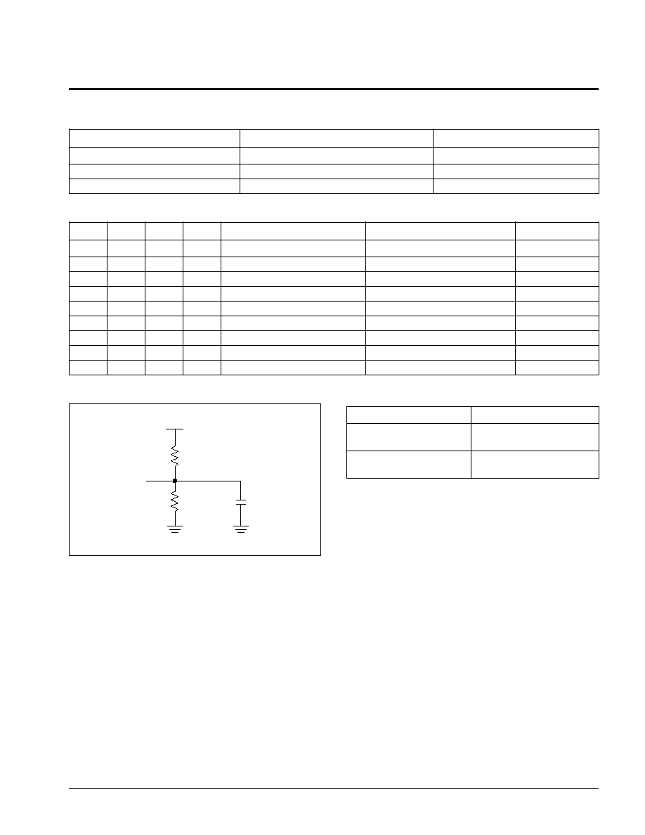
A.C. CONDITIONS OF TEST
Input Pulse Levels
0V to 3V
Input Rise and
Fall Times
5ns
Input and Output
Timing Levels
1.5V
3827 PGM T08.2
EQUIVALENT A.C. LOAD CIRCUIT
5V
735
318
OUTPUT
30pF
3827 FHD F04