Document Outline
- Table of Contents
- Product Selection
- Data Sheet Alpha
- Ap Note Alpha
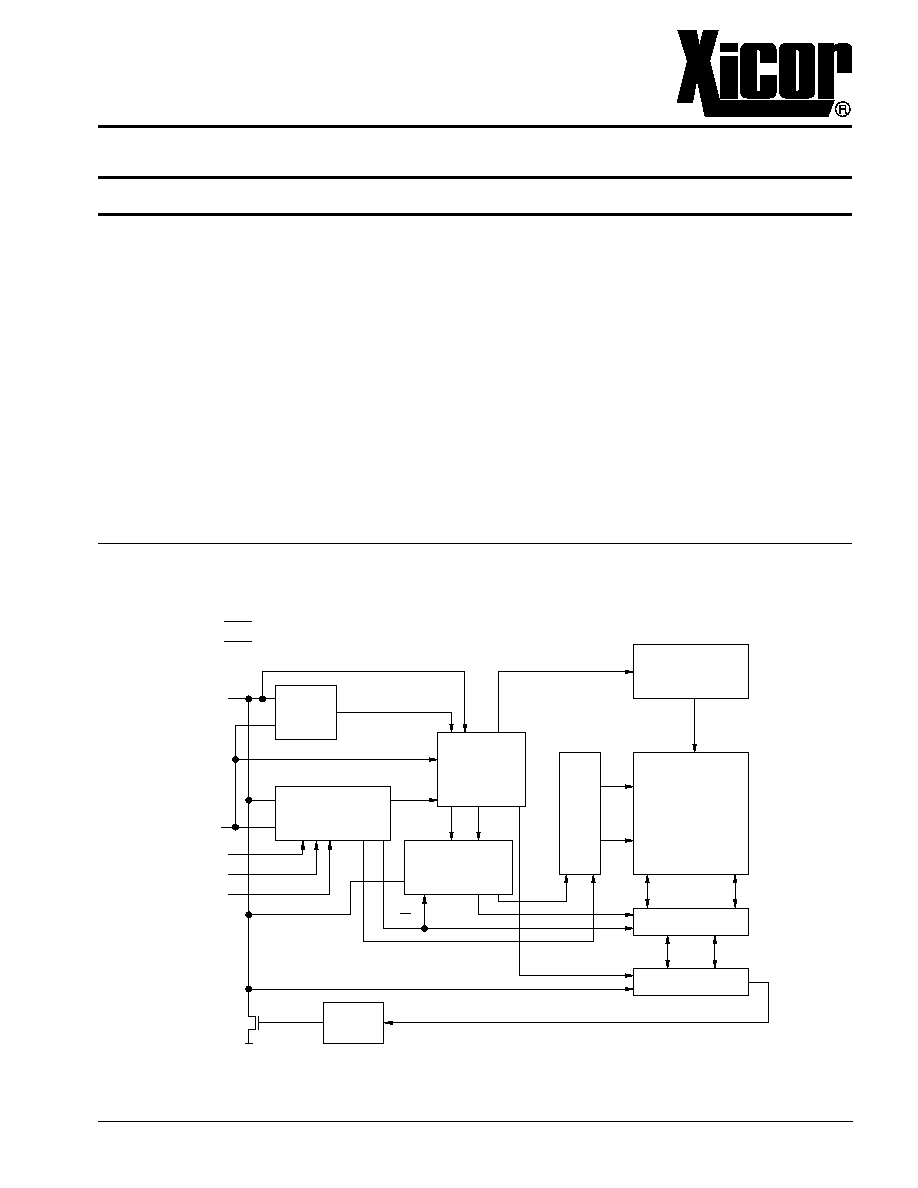
X24012
1
START
STOP
LOGIC
CONTROL
LOGIC
SLAVE ADDRESS
REGISTER
+COMPARATOR
H.V. GENERATION
TIMING
& CONTROL
WORD
ADDRESS
COUNTER
XDEC
YDEC
DOUT
ACK
E
2
PROM
32 X 32
DATA REGISTER
START CYCLE
(8) VCC
R/W
PIN
(4) VSS
(5) SDA
(6) SCL
(3) A2
(2) A1
(1) A0
DOUT
LOAD
INC
CK
8
DESCRIPTION
The X24012 is a CMOS 1024 bit serial E
2
PROM,
internally organized as one 128 x 8 bank. The X24012
features a serial interface and software protocol allow-
ing operation on a simple two wire bus. Three address
inputs allow up to eight devices to share a common two
wire bus.
Xicor E
2
PROMs are designed and tested for applica-
tions requiring extended endurance. Inherent data re-
tention is greater than 100 years. The X24012 is avail-
able in eight pin DIP and SOIC packages.
FEATURES
�
2.7 to 5.5V Power Supply
�
Low Power CMOS
--Active Current Less Than 1 mA
--Standby Current Less Than 50
�
A
�
Internally Organized 128 x 8
�
Self Timed Write Cycle
--Typical Write Cycle Time of 5 ms
�
2 Wire Serial Interface
--Bidirectional Data Transfer Protocol
�
Four Byte Page Write Operation
--Minimizes Total Write Time Per Byte
�
High Reliability
--Endurance: 100,000 Cycles
--Data Retention: 100 Years
� Xicor, 1991 Patents Pending
Characteristics subject to change without notice
1K
X24012
128 x 8 Bit
Serial E
2
PROM
FUNCTIONAL DIAGRAM
3847 FHD F01
Preliminary Information
Pin 7 No Connect
3847-1
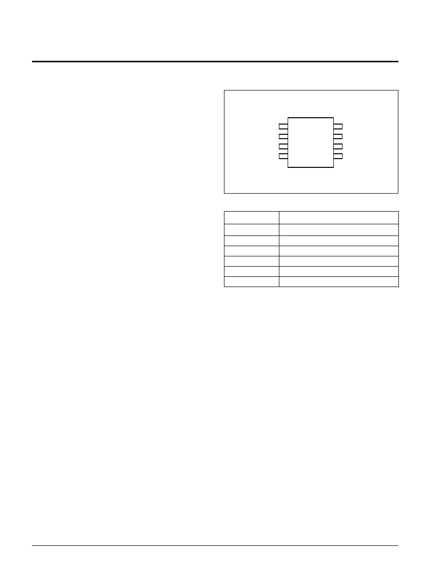
X24012
2
PIN CONFIGURATION
PIN NAMES
Symbol
Description
A
0
�A
2
Address Inputs
SDA
Serial Data
SCL
Serial Clock
NC
No Connect
V
SS
Ground
V
CC
+5V
3847 PGM T01
PIN DESCRIPTIONS
Serial Clock (SCL)
The SCL input is used to clock all data into and out of the
device.
Serial Data (SDA)
SDA is a bidirectional pin used to transfer data into and
out of the device. It is an open drain output and may be
wire-ORed with any number of open drain or open
collector outputs.
An open drain output requires the use of a pull-up
resistor. For selecting typical values, refer to the Guide-
lines for Calculating Typical Values of Bus Pull-Up
Resistors graph.
Address (A
0
, A
1
, A
2
)
The address inputs are used to set the least significant
three bits of the seven bit slave address. These inputs
can be static or actively driven. If used statically they
must be tied to V
SS
or V
CC
as appropriate. If actively
driven, they must be driven to V
SS
or to V
CC
.
3847 FHD F02
VCC
NC
SCL
SDA
A0
A1
A2
VSS
1
2
3
4
8
7
6
5
X24012
DIP/SOIC
X24012
3
DEVICE OPERATION
The X24012 supports a bidirectional bus oriented proto-
col. The protocol defines any device that sends data
onto the bus as a transmitter, and the receiving device
as the receiver. The device controlling the transfer is a
master and the device being controlled is the slave. The
master will always initiate data transfers and provide the
clock for both transmit and receive operations. There-
fore, the X24012 will be considered a slave in all
applications.
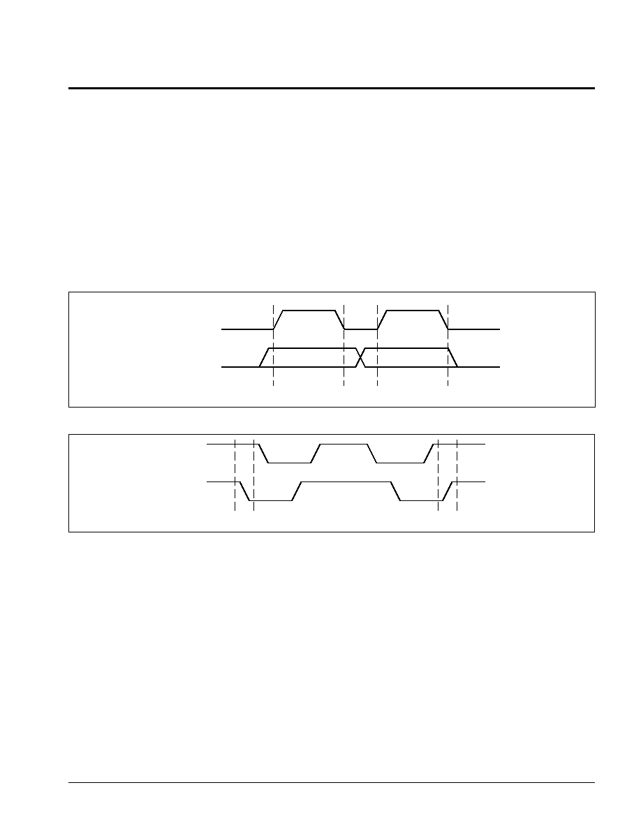
Clock and Data Conventions
Data states on the SDA line can change only during SCL
LOW. SDA state changes during SCL HIGH are re-
served for indicating start and stop conditions. Refer to
Figures 1 and 2.
Start Condition
All commands are preceded by the start condition,
which is a HIGH to LOW transition of SDA when SCL is
HIGH. The X24012 continuously monitors the SDA and
SCL lines for the start condition and will not respond to
any command until this condition has been met.
Figure 1. Data Validity
Figure 2. Definition of Start and Stop
SCL
SDA
DATA STABLE
DATA
CHANGE
SCL
SDA
START BIT
STOP BIT
3847 FHD F05
3847 FHD F06
X24012
4
Stop Condition
All communications must be terminated by a stop condi-
tion, which is a LOW to HIGH transition of SDA when SCL
is HIGH. The stop condition is also used by the X24012 to
place the device into the standby power mode after a read
sequence. A stop condition can only be issued after the
transmitting device has released the bus.
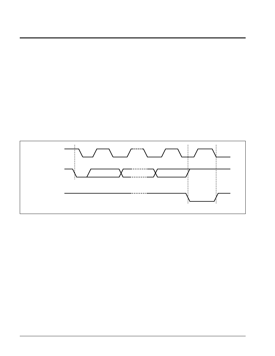
Acknowledge
Acknowledge is a software convention used to indicate
successful data transfers. The transmitting device will
release the bus after transmitting eight bits. During the
ninth clock cycle the receiver will pull the SDA line LOW
to acknowledge that it received the eight bits of data.
Refer to Figure 3.
The X24012 will respond with an acknowledge after
recognition of a start condition and its slave address. If
both the device and a write operation have been se-
lected, the X24012 will respond with an acknowledge
after the receipt of each subsequent eight bit word.
In the read mode the X24012 will transmit eight bits of
data, release the SDA line and monitor the line for an
acknowledge. If an acknowledge is detected and no
stop condition is generated by the master, the X24012
will continue to transmit data. If an acknowledge is not
detected, the X24012 will terminate further data trans-
missions. The master must then issue a stop condition
to return the X24012 to the standby power mode and
place the device into a known state.
Figure 3. Acknowledge Response From Receiver
3847 FHD F07
SCL FROM
MASTER
DATA
OUTPUT
FROM
TRANSMITTER
1
8
9
DATA
OUTPUT
FROM
RECEIVER
START
ACKNOWLEDGE
X24012
5
BUS ACTIVITY:
MASTER
SDA LINE
BUS ACTIVITY:
X24012
S
T
A
R
T
SLAVE
ADDRESS
S
S
T
O
P
P
A
C
K
A
C
K
A
C
K
A
C
K
A
C
K
WORD ADDRESS n
DATA n
DATA n�1
DATA n+3
NOTE: In this example n = xxxx 0000 (B); x = 1 or 0
BUS ACTIVITY:
MASTER
SDA LINE
BUS ACTIVITY:
X24012
S
T
A
R
T
SLAVE
ADDRESS
S
S
T
O
P
P
A
C
K
A
C
K
A
C
K
WORD
ADDRESS
DATA
DEVICE ADDRESSING
Following a start condition the master must output the
address of the slave it is accessing. The most significant
four bits of the slave address are the device type
identifier (see Figure 4). For the X24012 this is fixed as
1010[B].
Following the start condition, the X24012 monitors the
SDA bus comparing the slave address being transmit-
ted with its slave address (device type and state of A
0
,
A
1
and A
2
inputs). Upon a correct compare the X24012
outputs an acknowledge on the SDA line. Depending on
the state of the R/
W
bit, the X24012 will execute a read
or write operation.
WRITE OPERATIONS
Byte Write
For a write operation, the X24012 requires a second
address field. This address field is the word address,
comprised of eight bits, providing access to any one of
the 128 words of memory. Note: the most significant bit
is a don't care. Upon receipt of the word address the
X24012 responds with an acknowledge, and awaits the
next eight bits of data, again responding with an ac-
knowledge. The master then terminates the transfer by
generating a stop condition, at which time the X24012
begins the internal write cycle to the nonvolatile memory.
While the internal write cycle is in progress the X24012
inputs are disabled, and the device will not respond to
any requests from the master. Refer to Figure 5 for the
address, acknowledge and data transfer sequence.
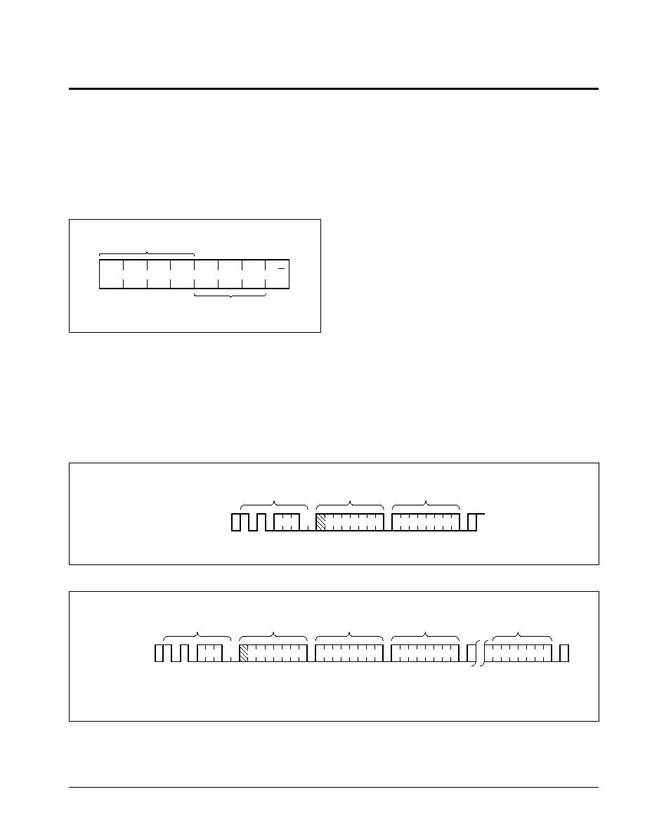
Figure 4. Slave Address
The next three significant bits address a particular
device. A system could have up to eight X24012 devices
on the bus (see Figure 10). The eight addresses are
defined by the state of the A
0
, A
1
and A
2
inputs.
The last bit of the slave address defines the operation to
be performed. When set to one a read operation is
selected, when set to zero a write operation is selected.
Figure 5. Byte Write
Figure 6. Page Write
1
0
1
0
A2
A1
A0
R/W
DEVICE TYPE
IDENTIFIER
DEVICE
ADDRESS
3847 FHD F08
3847 FHD F09
3847 FHD F10
BUS ACTIVITY:
MASTER
SDA LINE
BUS ACTIVITY:
X24012
BUS ACTIVITY:
MASTER
SDA LINE
BUS ACTIVITY:
X24012