
REV 1.1.3 10/23/00
Characteristics subject to change without notice.
1 of 17
www.xicor.com
256K
X24256
32K x 8 Bit
400kHz 2-Wire Serial EEPROM
FEATURES
∑ 400kHz 2-wire serial interface
--Schmitt trigger input noise suppression
--Output slope control for ground bounce noise
elimination
∑ Longer battery life with lower power
--Active read current less than 1mA
--Active write current less than 3mA
--Standby current less than 1µA
∑ 2.5V to 5.5V power supply
∑ 64-byte page write mode
--Minimizes total write time per word
∑ Internally organized 32K x 8
∑ Bidirectional data transfer protocol
∑ Self-timed write cycle
--Typical write cycle time of 5ms
∑ High reliability
--Endurance: 100,000 cycles
--Data retention: 100 years
∑ 8-lead XBGA
∑ 8-lead SOIC
∑ 14-lead TSSOP
DESCRIPTION
The X24256 is a CMOS Serial EEPROM, internally
organized 32K x 8. The device features a serial inter-
face and software protocol allowing operation on a
simple two wire bus.
Two device select inputs (S
0
≠S
1
) allow up to 4 devices
to share a common two wire bus.
These pins have internal pull downs, so they are read
as LOW if not connected.
A WP pin, when pulled HIGH prevents any nonvolatile
writes to the array. When not connected WP is pulled
LOW, so the device is not normally protected.
Xicor EEPROMs are designed and tested for applica-
tions requiring extended endurance. Inherent data
retention is greater than 100 years.
BLOCK DIAGRAM
Serial EEPROM Data
and Address (SDA)
SCL
S
1
S
0
WP
Command
Decode
and
Control
Logic
Write Protect
Control Logic
Device
Select
Logic
Page
Decode
Logic
Data Register
Y Decode Logic
Write Voltage
Control
Serial E
E
PROM
Array
32K x 8
X24256
Characteristics subject to change without notice.
2 of 17
REV 1.1.3 10/23/00
www.xicor.com
PIN DESCRIPTIONS
Serial Clock (SCL)
The SCL input is used to clock all data into and out of
the device.
Serial Data (SDA)
SDA is a bidirectional pin used to transfer data into and
out of the device. It is an open drain output and may be
wire-ORed with any number of open drain or open col-
lector outputs.
An open drain output requires the use of a pull-up
resistor. For selecting typical values, refer to the Pull-
up resistor selection graph at the end of this data
sheet.
Device Select (S
0
, S
1
)
The device select inputs (S
0
, S
1
) are used to set bits in
the slave address. This allows up to four devices to
share a common bus. These inputs can be static or
actively driven. If used statically they must be tied to
V
SS
or V
CC
as appropriate. If actively driven, they must
be driven with CMOS levels (driven to V
CC
or V
SS
) and
they must be constant between each start and stop
issued on the SDA bus. These pins have an active pull
down internally and will be sensed as low if the pin is
left unconnected.
Write Protect (WP)
WP must be constant between each start and stop
issued on the SDA bus and is always active (not
gated). The WP pin has an active pull down to disable
the write protection when the input is left floating. The
Write Protect input controls the Hardware Write Protect
feature. When held LOW, Protection is disabled and
the device operates normally. When this input is held
HIGH, the device is protected, preventing changes to
any and all locations in the EEPROM array.
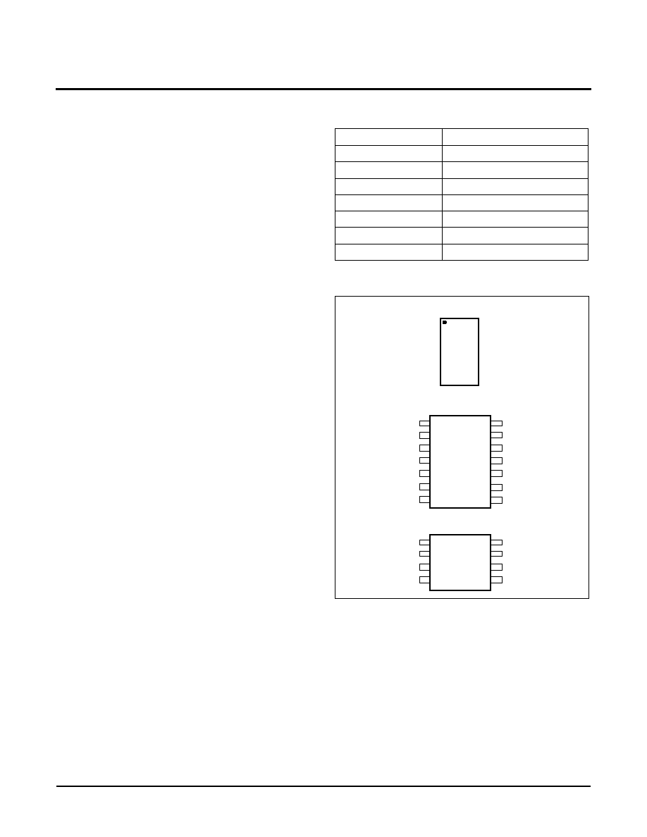
PIN NAMES
PIN CONFIGURATION
Symbol
Description
S
0
, S
1
Device Select Inputs
SDA
Serial Data
SCL
Serial Clock
WP
Write Protect
V
SS
Ground
V
CC
Supply Voltage
NC
No Connect
8-Lead SOIC
V
CC
WP
SCL
S
0
S
1
1
2
3
4
6
7
8
X24256
V
SS
SDA
S
2
5
14-Lead TSSOP
V
CC
WP
SCL
S
0
S
1
NC
1
2
3
4
7
6
5
X24256
V
SS
SDA
NC
NC
NC
NC
8
9
10
11
12
14
13
NC
S
1
SDA
NC
SCL
V
CC
V
SS
S
0
WP
8
7
6
5
1
2
3
4
S
2
8-Lead XBGA: Top View
X24256
Characteristics subject to change without notice.
3 of 17
REV 1.1.3 10/23/00
www.xicor.com
DEVICE OPERATION
The device supports a bidirectional bus oriented proto-
col. The protocol defines any device that sends data
onto the bus as a transmitter, and the receiving device
as the receiver. The device controlling the transfer is a
master and the device being controlled is the slave.
The master will always initiate data transfers, and pro-
vide the clock for both transmit and receive operations.
Therefore, the device will be considered a slave in all
applications.
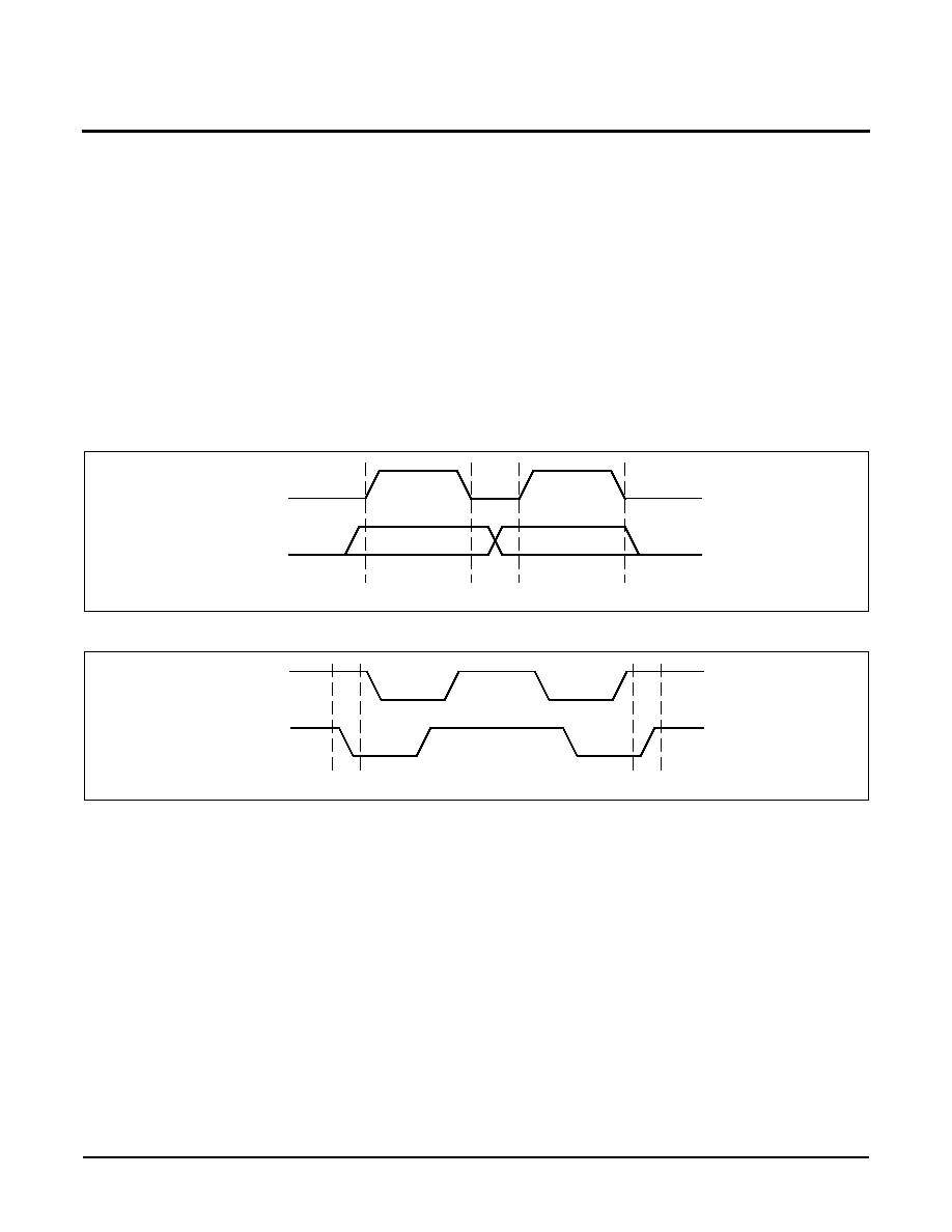
Clock and Data Conventions
Data states on the SDA line can change only during
SCL LOW. SDA state changes during SCL HIGH are
reserved for indicating start and stop conditions. Refer
to Figures 1 and 2.
Start Condition
All commands are preceded by the start condition,
which is a HIGH to LOW transition of SDA when SCL is
HIGH. The device continuously monitors the SDA and
SCL lines for the start condition and will not respond to
any command until this condition has been met.
Figure 1. Data Validity
Figure 2. Definition of Start and Stop
SCL
SDA
Data Stable
Data
Change
SCL
SDA
Start Bit
Stop Bit
Stop Condition
All communications must be terminated by a stop con-
dition, which is a LOW to HIGH transition of SDA when
SCL is HIGH. The stop condition is also used to place
the device into the standby power mode after a read
sequence. A stop condition can only be issued after
the transmitting device has released the bus.
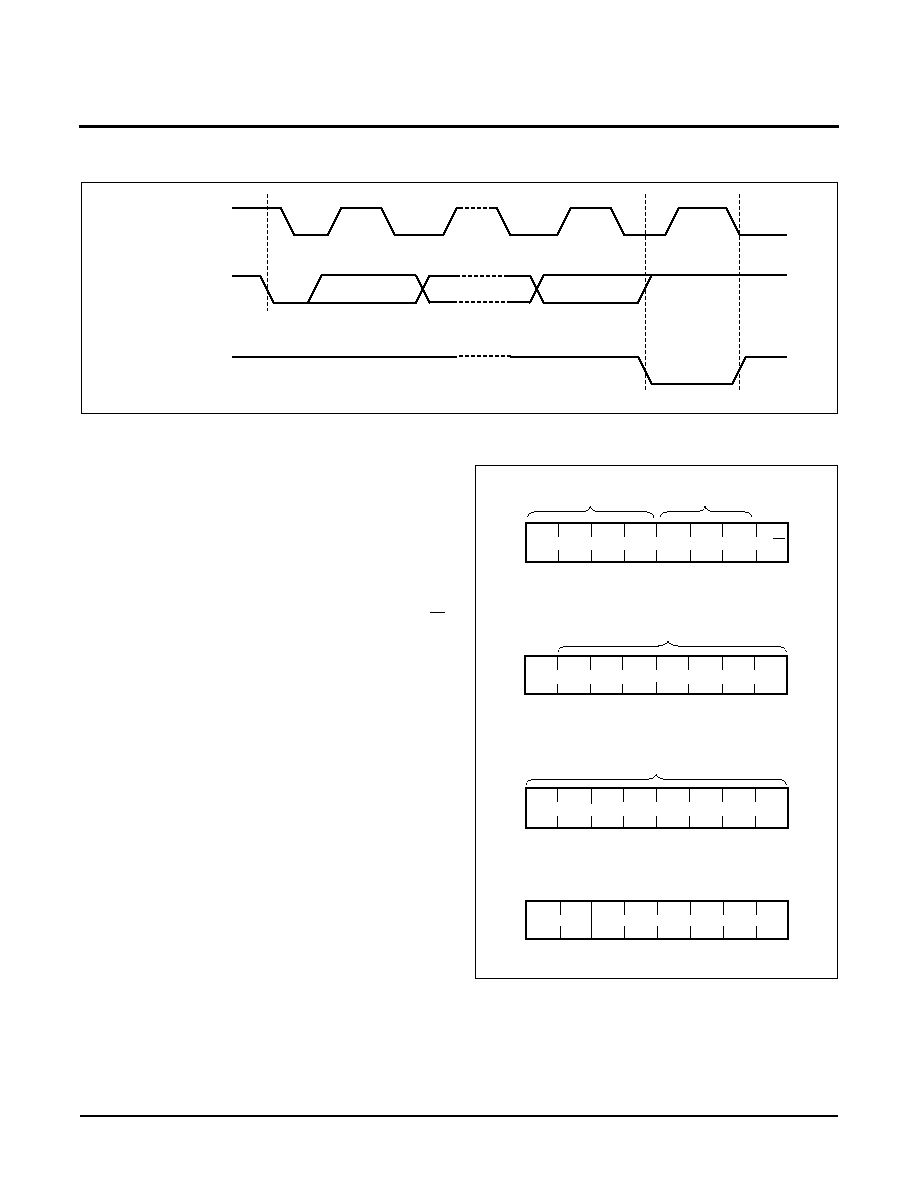
Acknowledge
Acknowledge is a software convention used to indicate
successful data transfer. The transmitting device, either
master or slave, will release the bus after transmitting
eight bits. During the ninth clock cycle the receiver will
pull the SDA line LOW to acknowledge that it received
the eight bits of data. Refer to Figure 3.
The device will respond with an acknowledge after rec-
ognition of a start condition and its slave address. If
both the device and a write operation have been
selected, the device will respond with an acknowledge
after the receipt of each subsequent 8-bit word.
In the read mode the device will transmit eight bits of
data, release the SDA line and monitor the line for an
acknowledge. If an acknowledge is detected and no
stop condition is generated by the master, the device
will continue to transmit data. If an acknowledge is not
detected, the device will terminate further data trans-
missions. The master must then issue a stop condition
to return the device to the standby power mode and
place the device into a known state.
X24256
Characteristics subject to change without notice.
4 of 17
REV 1.1.3 10/23/00
www.xicor.com
Figure 3. Acknowledge Response From Receiver
SCL from
Master
Data Output
from Transmitter
1
8
9
Data Output
from Receiver
Start
Acknowledge
DEVICE ADDRESSING
Following a start condition, the master must output the
address of the slave it is accessing. The first four bits of
the Slave Address Byte are the device type identifier
bits. These must equal "1010". The next bit is a "0". The
following 2 bits are the device select bits `0', S
1
and S
0
.
This allows up to 4 devices to share a single bus.
These bits are compared to the S
0
and S
1
device
select input pins. The last bit of the Slave Address Byte
defines the operation to be performed. When the R/W
bit is a one, then a read operation is selected. When it is
zero then a write operation is selected. Refer to Figure 4.
After loading the Slave Address Byte from the SDA bus,
the device compares the device type bits with the value
"1010" and the device select bits with the status of the
device select input pins. If the compare is not success-
ful, no acknowledge is output during the ninth clock
cycle and the device returns to the standby mode.
On power up the internal address is undefined, so the
first read or write operation must supply an address.
The word address is either supplied by the master or
obtained from an internal counter, depending on the
operation. The master must supply the two Word
Address Bytes as shown in Figure 4.
The internal organization of the E
2
array is 512 pages
by 64-bytes per page. The page address is partially
contained in the Word Address Byte 1 and partially in
bits 7 through 6 of the Word Address Byte 0. The byte
address is contained in bits 5 through 0 of the Word
Address Byte 0. See Figure 4.
Figure 4. Device Addressing
1
S
1
S
0
R/W
Device
Select
0
1
0
0
Device Type
Identifier
Slave Address Byte
D7
D2
D1
D6
D5
D4
D3
Data Byte
A2
A1
A0
A5
A4
A3
Word Address Byte 0
0
A10
A9
A8
A14
High Order Word Address
A11
X24256 Word Address Byte 1
A13
A12
A7
A6
D0
Low Order Word Address
X24256
Characteristics subject to change without notice.
5 of 17
REV 1.1.3 10/23/00
www.xicor.com
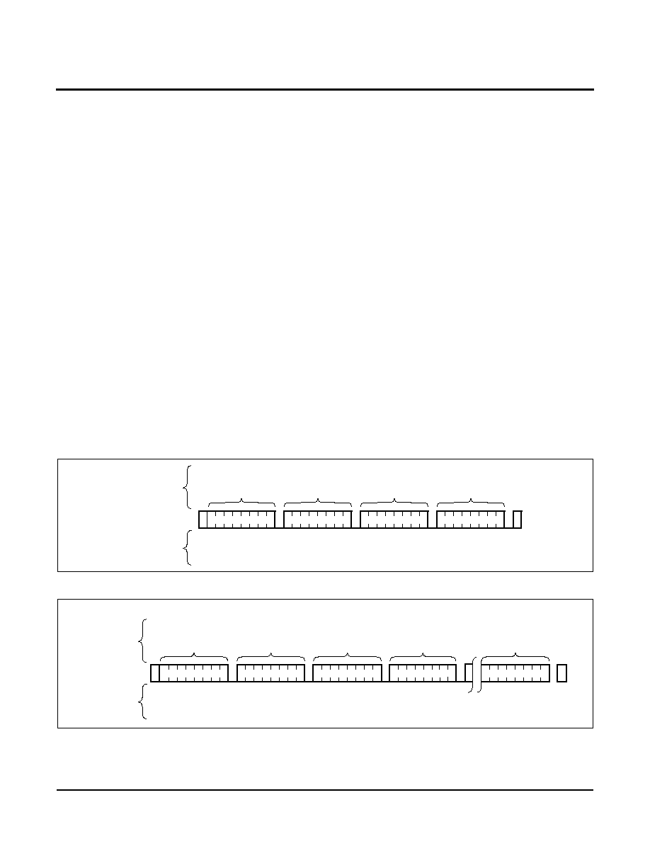
WRITE OPERATIONS
Byte Write
For a write operation, the device follows "3 byte" proto-
col, consisting of one Slave Address Byte, one Word
Address Byte 1, and the Word Address Byte 0, which
gives the master access to any one of the words in the
array. Upon receipt of the Word Address Byte 0, the
device responds with an acknowledge, and waits for
the first eight bits of data. After receiving the 8 bits of
the data byte, the device again responds with an
acknowledge. The master then terminates the transfer
by generating a stop condition, at which time the
device begins the internal write cycle to the nonvolatile
memory. While the internal write cycle is in progress
the device inputs are disabled and the device will not
respond to any requests from the master. The SDA pin
is at high impedance. See Figure 5.
Page Write
The device is capable of a 64 byte page write operation.
It is initiated in the same manner as the byte write
operation; but instead of terminating the write operation
after the first data word is transferred, the master can
transmit up to sixty-three more words. The device will
respond with an acknowledge after the receipt of each
word, and then the byte address is internally incre-
mented by one. The page address remains constant.
When the counter reaches the end of the page, it "rolls
over" and goes back to the first byte of the current
page. This means that the master can write 64-bytes to
the page beginning at any byte. If the master begins
writing at byte 32, and loads 64-bytes, then the first
32-bytes are written to bytes 32 through 63, and the
last 16 words are written to bytes 0 through 31. After-
wards, the address counter would point to byte 32. If the
master writes more than 64-bytes, then the previously
loaded data is overwritten by the new data, one byte at
a time.
The master terminates the data byte loading by issuing
a stop condition, which causes the device to begin the
nonvolatile write cycle. As with the byte write operation,
all inputs are disabled until completion of the internal
write cycle. Refer to Figure 6 for the address, acknowl-
edge, and data transfer sequence.
Figure 5. Byte Write Sequence
Figure 6. Page Write Sequence
Signals from
the Master
SDA Bus
Signals from
the Slave
S
T
A
R
T
Slave
Address
S
T
O
P
A
C
K
A
C
K
A
C
K
A
C
K
Word Address
Byte 1
Data
1 0 1 0 0
Byte 0
S
P
0
Word Address
S
1
S
0
S
T
A
R
T
S
T
O
P
A
C
K
A
C
K
A
C
K
A
C
K
A
C
K
Data
(0)
(n)
S
P
Data
1 0 1 0
0
(0
n
64)
Slave
Address
Word Address
Byte 1
Byte 0
Word Address
Signals from
the Master
SDA Bus
Signals from
the Slave
0
S
1
S
0