
©
Xicor, Inc. 2000 Patents Pending
6552-2.4 10/27/00 EP
Characteristics subject to change without notice.
1 of 18
32K
X24325
4096 x 8 Bit
Advanced 2-Wire Serial E
2
PROM with Block Lock
TM
Protection
FEATURES
∑ 2.7V to 5.5V Power Supply
∑ Low Power CMOS
--Active read current less than 1mA
--Active write current less than 3mA
--Standby current less than 1µA
∑ Internally Organized 4096 x 8
∑ New Programmable Block Lock Protection
--Software write protection
--Programmable hardware write protect
∑ Block Lock (0, 1/4, 1/2, or all of the E
2
PROM Array)
∑ 2 Wire Serial Interface
∑ Bidirectional Data Transfer Protocol
∑ 32 Byte Page Write Mode
--Minimizes total write time per byte
∑ Self Timed Write Cycle
--Typical write cycle time of 5ms
∑ High Reliability
--Endurance: 100,000 cycles
--Data retention: 100 years
∑ Available Packages
--8-lead PDIP
--8-lead SOIC (JEDEC)
--14-lead TSSOP
DESCRIPTION
The X24325 is a CMOS 32,768 bit serial E
2
PROM,
internally organized 4096 x 8. The X24325 features a
serial interface and software protocol allowing opera-
tion on a simple two wire bus.
Three device select inputs (S
0
, S
1
, S
2
) allow up to
eight devices to share a common two wire bus.
A Write Protect Register at the highest address location,
FFFh, provides three new write protection features: Soft-
ware Write Protect, Block Write Protect, and Hardware
Write Protect. The Software Write Protect feature pre-
vents any nonvolatile writes to the X24325 until the WEL
bit in the write protect register is set. The Block Write Pro-
tection feature allows the user to individually write protect
four blocks of the array by programming two bits in the
write protect register. The Programmable Hardware Write
Protect feature allows the user to install the X24325 with
WP tied to V
CC
, program the entire memory array in
place, and then enable the hardware write protection by
programming a WPEN bit in the write protect register.
After this, selected blocks of the array, including the write
protect register itself, are permanently write protected.
Xicor E
2
PROMs are designed and tested for applica-
tions requiring extended endurance. Inherent data
retention is greater than 100 years.
Preliminary Information

X24325
Characteristics subject to change without notice.
2 of 18
BLOCK DIAGRAM
H.V. Generation
Timing & Control
START Cycle
WP
V
CC
V
SS
SDA
SCL
S
0
S
1
S
2
START
STOP
Logic
Slave Address
Register
+ Comparator
Control
Logic
Word
Address
Counter
PIN
CK
D
OUT
ACK
R/W
LOAD
INC
XDEC
E
2
PROM
128 X 256
Write Protect
Register
and Logic
YDEC
8
Data Register
PIN DESCRIPTIONS
Serial Clock (SCL)
The SCL input is used to clock all data into and out of
the device.
Serial Data (SDA)
SDA is a bidirectional pin used to transfer data into and
out of the device. It is an open drain output and may be
wire-ORed with any number of open drain or open col-
lector outputs.
An open drain output requires the use of a pull-up
resistor. For selecting typical values, refer to the Pull-
Up Resistor selection graph at the end of this data
sheet.
Device Select (S
0
, S
1
, S
2
)
The device select inputs (S
0
, S
1
, S
2
) are used to set
the first three bits of the 8-bit slave address. This
allows up to eight X24325's to share a common bus.
These inputs can be static or actively driven. If used
statically they must be tied to V
SS
or V
CC
as appropri-
ate. If actively driven, they must be driven with CMOS
levels (driven to V
CC
or V
SS
).
Write Protect (WP)
The write protect input controls the hardware write pro-
tect feature. When held LOW, hardware write protec-
tion is disabled and the X24325 can be written
normally.
When this input is held HIGH, and the WPEN
bit in the write protect register is set HIGH, write pro-
tection is enabled, and nonvolatile writes are disabled
to the selected blocks as well as the write protect regis-
ter itself.

X24325
Characteristics subject to change without notice.
3 of 18
PIN NAMES
PIN CONFIGURATIONS
DEVICE OPERATION
The X24325 supports a bidirectional bus oriented pro-
tocol. The protocol defines any device that sends data
onto the bus as a transmitter, and the receiving device
as the receiver. The device controlling the transfer is a
master and the device being controlled is the slave.
The master will always initiate data transfers, and pro-
vide the clock for both transmit and receive operations.
Therefore, the X24325 will be considered a slave in all
applications.
Clock and Data Conventions
Data states on the SDA line can change only during
SCL LOW. SDA state changes during SCL HIGH are
reserved for indicating start and stop conditions. Refer
to Figures 1 and 2.
Start Condition
All commands are preceded by the start condition,
which is a HIGH to LOW transition of SDA when SCL is
HIGH. The X24325 continuously monitors the SDA and
SCL lines for the start condition and will not respond to
any command until this condition has been met.
Symbol
Description
S
0
, S
1
,
S
2
Device Select Inputs
SDA
Serial Data
SCL
Serial Clock
WP
Write Protect
V
SS
Ground
V
CC
Supply Voltage
NC
No Connect
V
CC
WP
SCL
SDA
S
0
S
1
S
2
V
SS
1
2
3
4
8
7
6
5
X24325
8-Lead PDIP/SOIC
S
0
S
1
NC
NC
NC
S
2
V
SS
V
CC
WP
NC
NC
NC
SCL
SDA
1
2
3
4
5
6
7
14
13
12
11
10
9
8
X24325
14-Lead TSSOP
Figure 1. Data Validity
SCL
SDA
Data Stable
Data
Change

X24325
Characteristics subject to change without notice.
4 of 18
Figure 2. Definition of Start and Stop
SCL
SDA
START Bit
STOP Bit
Stop Condition
All communications must be terminated by a stop con-
dition, which is a LOW to HIGH transition of SDA when
SCL is HIGH. The stop condition is also used to place
the device into the standby power mode after a read
sequence. A stop condition can only be issued after
the transmitting device has released the bus.
Acknowledge
Acknowledge is a software convention used to indicate
successful data transfer. The transmitting device, either
master or slave, will release the bus after transmitting
eight bits. During the ninth clock cycle the receiver will
pull the SDA line LOW to acknowledge that it received
the eight bits of data. Refer to Figure 3.
The X24325 will respond with an acknowledge after
recognition of a start condition and its slave address. If
both the device and a write operation have been
selected, the X24325 will respond with an acknowl-
edge after the receipt of each subsequent eight-bit
word.
In the read mode the X24325 will transmit eight bits of
data, release the SDA line and monitor the line for an
acknowledge. If an acknowledge is detected and no
stop condition is generated by the master, the X24325
will continue to transmit data. If an acknowledge is not
detected, the X24325 will terminate further data trans-
missions. The master must then issue a stop condition
to return the X24325 to the standby power mode and
place the device into a known state.
Figure 3. Acknowledge Response From Receiver
SCL From
Master
Data Output
From Transmitter
1
8
9
Data Output
From Receiver
START
Acknowledge
X24325
Characteristics subject to change without notice.
5 of 18
DEVICE ADDRESSING
Following a start condition the master must output the
address of the slave it is accessing (see Figure 4). The
next three bits are the device select bits. A system
could have up to eight X24325's on the bus. The eight
addresses are defined by the state of the S
0
, S
1
and S
2
inputs. S
0
and S
2
of the slave address must be the
inverse of the S
0
and S
2
input pins.
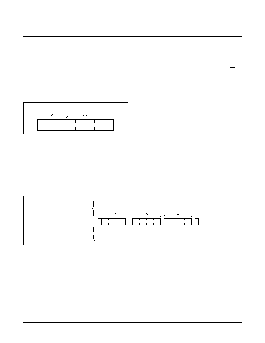
Figure 4. Slave Address
The next four bits of the slave address are an exten-
sion of the array's address and are concatenated with
the eight bits of address in the word address field, pro-
viding direct access to the whole 4096 x 8 array.
The last bit of the slave address defines the operation
to be performed. When set HIGH a read operation is
selected, when set LOW a write operation is selected.
Following the start condition, the X24325 monitors the
SDA bus comparing the slave address being transmit-
ted with its slave address device type identifier. Upon a
correct compare the X24325 outputs an acknowledge
on the SDA line. Depending on the state of the R/W bit,
the X24325 will execute a read or write operation.
WRITE OPERATIONS
Byte Write
For a write operation, the X24325 requires a second
address field. This address field is the word address,
comprised of eight bits, providing access to any one of
4096 words in the array. Upon receipt of the word
address, the X24325 responds with an acknowledge
and awaits the next eight bits of data, again responding
with an acknowledge. The master then terminates the
transfer by generating a stop condition, at which time
the X24325 begins the internal write cycle to the non-
volatile memory. While the internal write cycle is in
progress the X24325 inputs are disabled, and the
device will not respond to any requests from the mas-
ter. Refer to Figure 5 for the address, acknowledge and
data transfer sequence.
S
2
A9
A8
R/W
High Order
Word Adress
S
1
S
0
A11
A10
Device
Select
Figure 5. Byte Write Sequence
Signals From
The Master
SDA Bus
Signals From
S
T
A
R
T
Slave
Address
S
T
O
P
A
C
K
A
C
K
A
C
K
Word
Data
S
P
The Slave
Address
Page Write
The X24325 is capable of a 32 byte page write opera-
tion. It is initiated in the same manner as the byte write
operation, but instead of terminating the write cycle
after the first data word is transferred, the master can
transmit up to fifteen more words. After the receipt of
each word, the X24325 will respond with an acknowl-
edge.
After the receipt of each word, the five low order
address bits are internally incremented by one. The
high order bits of the word address remain constant. If
the master should transmit more than 32 words prior to
generating the stop condition, the address counter will
"roll over" and the previously written data will be over-
written. As with the byte write operation, all inputs are
disabled until completion of the internal write cycle.
Refer to Figure 6 for the address, acknowledge and
data transfer sequence.