 | –≠–ª–µ–∫—Ç—Ä–æ–Ω–Ω—ã–π –∫–æ–º–ø–æ–Ω–µ–Ω—Ç: X24C01-3 | –°–∫–∞—á–∞—Ç—å:  PDF PDF  ZIP ZIP |
X24C01
1
Serial E
2
PROM
© Xicor, 1991 Patents Pending
Characteristics subject to change without notice
Preliminary Information
DESCRIPTION
The X24C01 is a CMOS 1024 bit serial E
2
PROM,
internally organized as 128 x 8. The X24C01 features a
serial interface and software protocol allowing operation
on a simple two wire bus.
Xicor E
2
PROMs are designed and tested for applica-
tions requiring extended endurance. Inherent data re-
tention is greater than 100 years.
FEATURES
∑
2.7V to 5.5V Power Supply
∑
Low Power CMOS
--Active Current Less Than 1 mA
--Standby Current Less Than 50 µA
∑
Internally Organized 128 x 8
∑
2 Wire Serial Interface
--Bidirectional Data Transfer Protocol
∑
Four Byte Page Write Mode
∑
Self Timed Write Cycle
--Typical Write Cycle Time of 5 ms
∑
High Reliability
--Endurance: 1 Million Cycles
--Data Retention: 100 Years
∑
8-Pin Mini-DIP, 8-PIN MSOP, and 8-PIN SOIC
Packages
1K
X24C01
128 x 8 Bit
3837 FHD F01
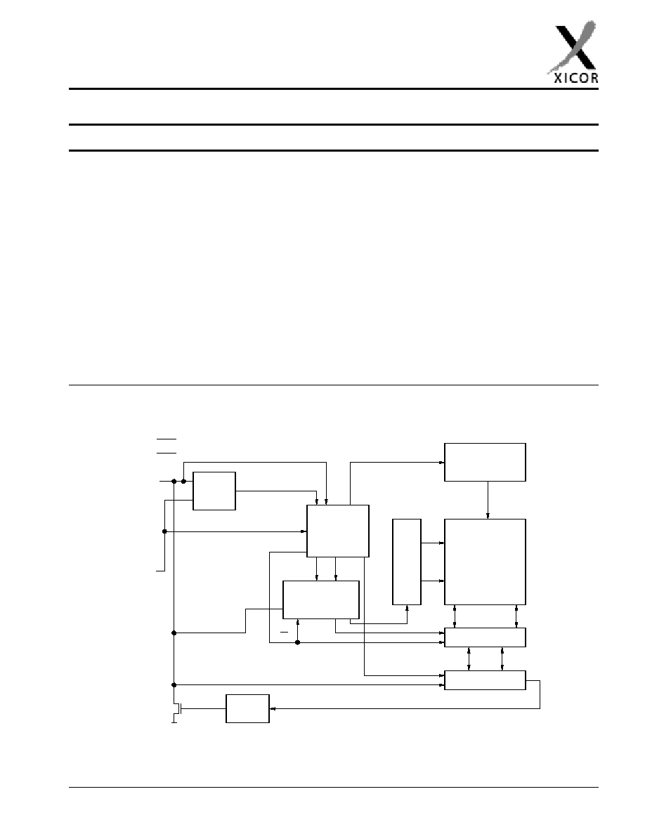
FUNCTIONAL DIAGRAM
START
STOP
LOGIC
CONTROL
LOGIC
H.V. GENERATION
TIMING
& CONTROL
WORD
ADDRESS
COUNTER
XDEC
YDEC
DOUT
ACK
E
2
PROM
32 X 32
DATA REGISTER
START CYCLE
(8) VCC
R/W
PIN
(4) VSS
(5) SDA
(6) SCL
DOUT
LOAD
INC
CK
8
3837-1.2 2/24/99 T1/C0/D0 SH
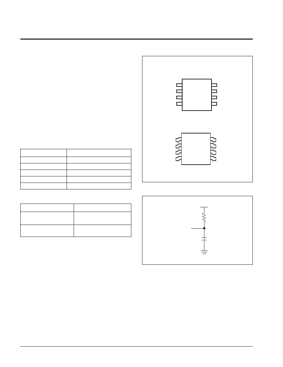
2
X24C01
NC
NC
NC
VSS
1
2
3
4
8
7
6
5
VCC
NC
SCL
SDA
X24C01
PLASTIC
PIN CONFIGURATION
PIN DESCRIPTIONS
Serial Clock (SCL)
The SCL input is used to clock all data into and out of the
device.
Serial Data (SDA)
SDA is a bidirectional pin used to transfer data into and
out of the device. It is an open drain output and may be
wire-ORed with any number of open drain or open
collector outputs.
An open drain output requires the use of a pull-up
resistor. For selecting typical values, refer to the Guide-
lines for Calculating Typical Values of Bus Pull-Up
Resistors graph.
PIN NAMES
Symbol
Description
NC
No Connect
V
SS
Ground
V
CC
Supply Voltage
SDA
Serial Data
SCL
Serial Clock
3837 PGM T01
A.C. CONDITIONS OF TEST
Input Pulse Levels
V
CC
x 0.1 to V
CC
x 0.9
Input Rise and
Fall Times
10 ns
Input and Output
Timing Levels
V
CC
x 0.5
3837 PGM T02
3837 FHD F02
3837 FHD F03
EQUIVALENT A.C. LOAD CIRCUIT
3837 FHD F16
2190
100pF
OUTPUT
5V
DIP
NC
NC
NC
VSS
1
2
3
4
8
7
6
5
VCC
NC
SCL
SDA
X24C01
SOIC/MSOP

X24C01
3
DEVICE OPERATION
The X24C01 supports a bidirectional bus oriented pro-
tocol. The protocol defines any device that sends data
onto the bus as a transmitter and the receiving device as
the receiver. The device controlling the transfer is a
master and the device being controlled is the slave. The
master will always initiate data transfers and provide the
clock for both transmit and receive operations. There-
fore, the X24C01 will be considered a slave in all
applications.
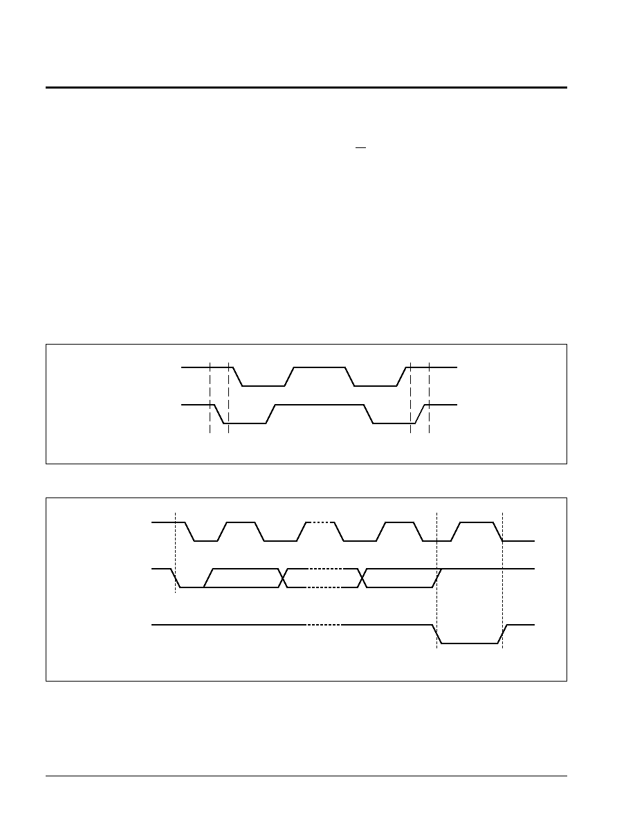
Clock and Data Conventions
Data states on the SDA line can change only during SCL
LOW. SDA state changes during SCL HIGH are re-
served for indicating start and stop conditions. Refer to
Figures 1 and 2.
Start Condition
All commands are preceded by the start condition,
which is a HIGH to LOW transition of SDA when SCL is
HIGH. The X24C01 continuously monitors the SDA and
SCL lines for the start condition and will not respond to
any command until this condition has been met.
Figure 1. Data Validity
SCL
SDA
DATA STABLE
DATA
CHANGE
3837 FHD F06
4
X24C01
Stop Condition
All communications must be terminated by a stop con-
dition, which is a LOW to HIGH transition of SDA when
SCL is HIGH. The stop condition is also used by the
X24C01 to place the device in the standby power mode
after a read sequence. A stop condition can only be
issued after the transmitting device has released the
bus.
Acknowledge
Acknowledge is a software convention used to indicate
successful data transfers. The transmitting device will
release the bus after transmitting eight bits. During the
ninth clock cycle the receiver will pull the SDA line LOW
to acknowledge that it received the eight bits of data.
Refer to Figure 3.
The X24C01 will respond with an acknowledge after
recognition of a start condition, a seven bit word address
and a R/W bit. If a write operation has been selected, the
X24C01 will respond with an acknowledge after each
byte of data is received.
In the read mode the X24C01 will transmit eight bits of
data, release the SDA line and monitor the line for an
acknowledge. If an acknowledge is detected and no
stop condition is generated by the master, the X24C01
will continue to transmit data. If an acknowledge is not
detected, the X24C01 will terminate further data trans-
missions. The master must then issue a stop condition
to return the X24C01 to the standby power mode and
place the device into a known state.
Figure 2. Definition of Start and Stop
3837 FHD F07
Figure 3. Acknowledge Response From Receiver
SCL FROM
MASTER
DATA
OUTPUT
FROM
TRANSMITTER
1
8
9
DATA
OUTPUT
FROM
RECEIVER
START
ACKNOWLEDGE
3837 FHD F08
SCL
SDA
START CONDITION
STOP CONDITION
X24C01
5
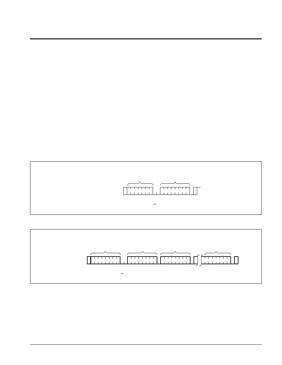
WRITE OPERATIONS
Byte Write
To initiate a write operation, the master sends a start
condition followed by a seven bit word address and a write
bit. The X24C01 responds with an acknowledge, then
waits for eight bits of data and then responds with an
acknowledge. The master then terminates the transfer by
generating a stop condition, at which time the X24C01
begins the internal write cycle to the nonvolatile memory.
While the internal write cycle is in progress, the X24C01
inputs are disabled, and the device will not respond to any
requests from the master. Refer to Figure 4 for the
address, acknowledge and data transfer sequence.
Page Write
The most significant five bits of the word address define
the page address. The X24C01 is capable of a four byte
page write operation. It is initiated in the same manner as
the byte write operation, but instead of terminating the
transfer of data after the first data byte, the master can
transmit up to three more bytes. After the receipt of each
data byte, the X24C01 will respond with an acknowledge.
After the receipt of each data byte, the two low order
address bits are internally incremented by one. The high
order five bits of the address remain constant. If the
master should transmit more than four data bytes prior
to generating the stop condition, the address counter will
"roll over" and the previously transmitted data will be
overwritten. As with the byte write operation, all inputs
are disabled until completion of the internal write cycle.
Refer to Figure 5 for the address, acknowledge and data
transfer sequence.
BUS ACTIVITY:
SDA LINE
BUS ACTIVITY:
X24C01
S
T
A
R
T
WORD
ADDRESS (n)
S
T
O
P
P
A
C
K
DATA n
R
/
W
L
S
B
S
M
S
B
A
C
K
3837 FHD F09
Figure 5. Page Write
BUS ACTIVITY:
SDA LINE
BUS ACTIVITY:
X24C01
S
T
A
R
T
S
S
T
O
P
P
A
C
K
A
C
K
A
C
K
M
S
B
WORD
ADDRESS (n)
DATA n
DATA n+1
DATA n+3
A
C
K
R
/
W
L
S
B
3837 FHD F10
6
X24C01
Figure 6. ACK Polling Sequence
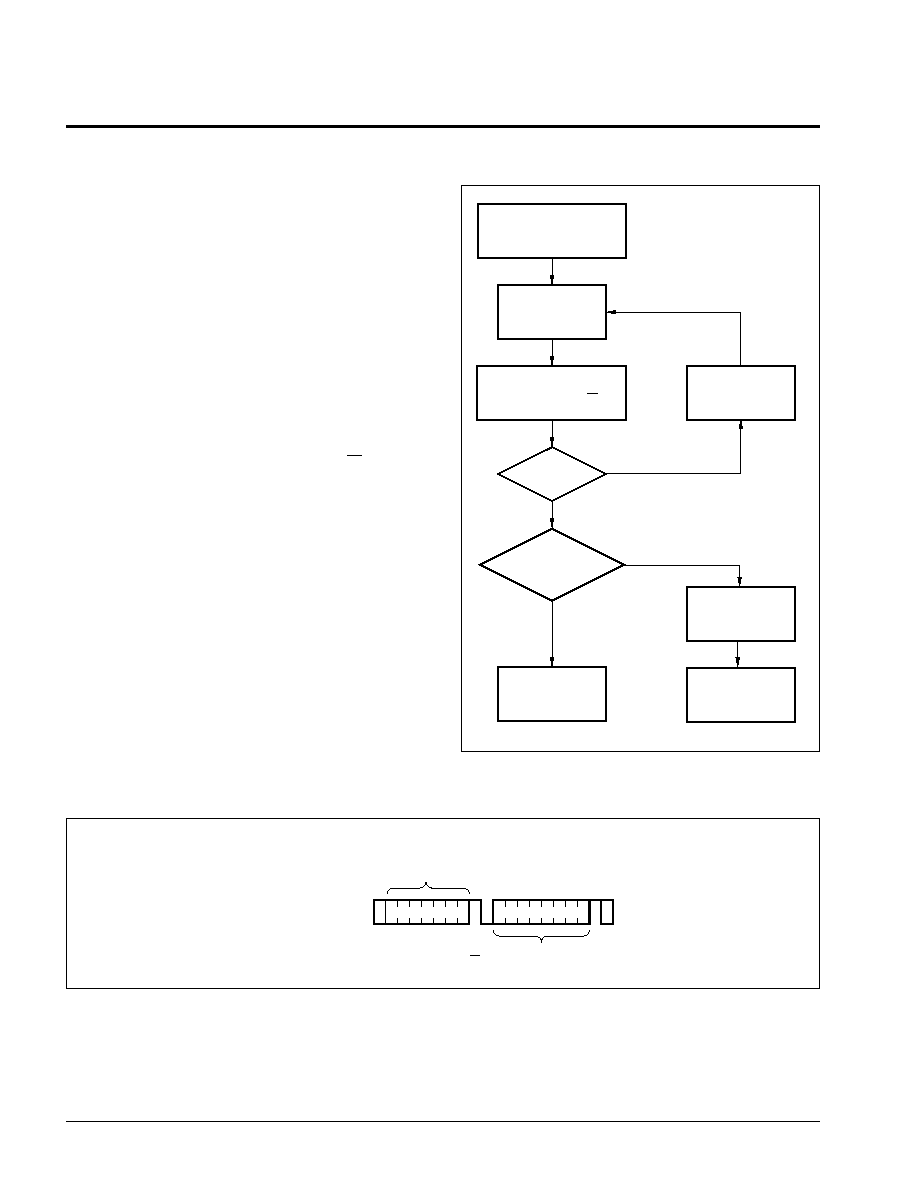
Acknowledge Polling
The disabling of the inputs can be used to take advan-
tage of the typical 5 ms write cycle time. Once the stop
condition is issued to indicate the end of the host's write
operation the X24C01 initiates the internal write cycle.
ACK polling can be initiated immediately. This involves
issuing the start condition followed by the word address
for a write operation. If the X24C01 is still busy with the
write operation no ACK will be returned. If the X24C01
has completed the write operation an ACK will be
returned and the controller can then proceed with the
next read or write operation.
READ OPERATIONS
Read operations are initiated in the same manner as
write operations with exception that the R/W bit of the
word address is set to a one. There are two basic read
operations: byte read and sequential read.
It should be noted that the ninth clock cycle of the read
operation is not a "don't care." To terminate a read
operation, the master must either issue a stop condition
during the ninth cycle or hold SDA HIGH during the ninth
clock cycle and then issue a stop condition.
Byte Read
To initiate a read operation, the master sends a start
condition followed by a seven bit word address and a
read bit. The X24C01 responds with an acknowledge
and then transmits the eight bits of data. The read
operation is terminated by the master; by not responding
with an acknowledge and by issuing a stop condition.
Refer to Figure 7 for the start, word address, read bit,
acknowledge and data transfer sequence.
WRITE OPERATION
COMPLETED
ENTER ACK POLLING
ISSUE
START
ISSUE SLAVE
ADDRESS AND R/W = 0
ACK
RETURNED?
NEXT
OPERATION
A WRITE?
PROCEED
ISSUE STOP
NO
YES
YES
PROCEED
ISSUE STOP
NO
3837 FHD F11
Figure 7. Byte Read
3837 FHD F12
BUS ACTIVITY:
MASTER
SDA LINE
BUS ACTIVITY:
X24C01
S
T
A
R
T
WORD
ADDRESS n
S
T
O
P
P
A
C
K
DATA n
R
/
W
L
S
B
S
M
S
B
X24C01
7
Sequential Read
Sequential read is initiated in the same manner as the
byte read. The first data byte is transmitted as with the
byte read mode, however, the master now responds
with an acknowledge, indicating it requires additional
data. The X24C01 continues to output data for each
acknowledge received. The read operation is termi-
nated by the master; by not responding with an acknowl-
edge and by issuing a stop condition.
The data output is sequential, with the data from address
n followed by the data from n + 1. The address counter
for read operations increments all address bits, allowing
the entire memory contents to be serially read during
one operation. At the end of the address space (address
127) the counter "rolls over" to zero and the X24C01
continues to output data for each acknowledge re-
ceived. Refer to Figure 8 for the address, acknowledge
and data transfer sequence.
Figure 8. Sequential Read
3837 FHD F13
Figure 9. Typical System Configuration
BUS ACTIVITY:
SDA LINE
BUS ACTIVITY:
X24C01
ADDRESS
A
C
K
A
C
K
DATA n+x
S
T
O
P
P
DATA n
A
C
K
DATA n+1
A
C
K
DATA n+2
R
/
W
MASTER
TRANSMITTER/
RECEIVER
SLAVE
RECEIVER
SLAVE
TRANSMITTER/
RECEIVER
MASTER
TRANSMITTER
MASTER
TRANSMITTER/
RECEIVER
PULL-UP
RESISTORS
SDA
SCL
VCC
3837 FHD 14
8
X24C01
Supply Voltage
Limits
X24C01
4.5V to 5.5V
X24C01-3.5
3.5V to 5.5V
X24C01-3
3.0V to 5.5V
X24C01-2.7
2.7V to 5.5V
ABSOLUTE MAXIMUM RATINGS*
Temperature Under Bias .................. ≠65∞C to +135∞C
Storage Temperature ....................... ≠65∞C to +150∞C
Voltage on any Pin with
Respect to V
SS
............................ ≠1.0V to +7.0V
D.C. Output Current ............................................ 5 mA
Lead Temperature
(Soldering, 10 Seconds) ............................. 300∞C
*COMMENT
Stresses above those listed under "Absolute Maximum
Ratings" may cause permanent damage to the device.
This is a stress rating only and the functional operation of
the device at these or any other conditions above those
indicated in the operational sections of this specification is
not implied. Exposure to absolute maximum rating condi-
tions for extended periods may affect device reliability.
RECOMMENDED OPERATING CONDITIONS
Temperature
Min.
Max.
Commercial
0∞C
70∞C
Industrial
≠40∞C
+85∞C
Military
≠55∞C
+125∞C
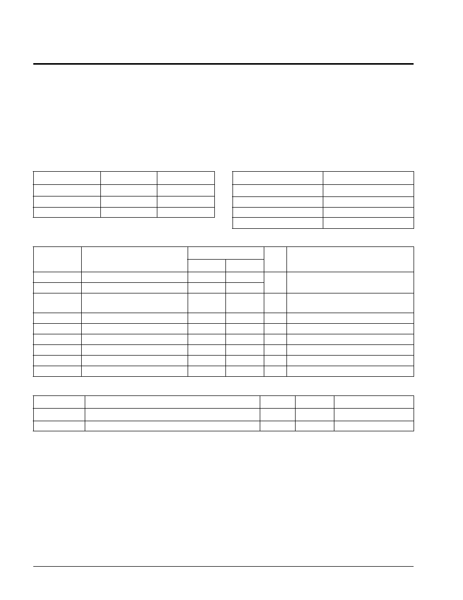
D.C. OPERATING CHARACTERISTICS (Over recommended operating conditions, unless otherwise specified)
Limits
Symbol
Parameter
Min.
Max.
Units
Test Conditions
I
CC
(1)
V
CC
Supply Current (Read)
1
mA
SCL = V
CC
x 0.1/V
CC
x 0.9 Levels
I
CC
(2)
V
CC
Supply Current (Write)
2
@ 100 KHz, SDA = Open
I
SB1
(1)
V
CC
Standby Current
100
µA
SCL = SDA = V
CC
,
V
CC
= 5V ± 10%
I
SB2
(1)
V
CC
Standby Current
50
µA
SCL = SDA = V
CC
, V
CC
= 2.7V
I
LI
Input Leakage Current
10
µA
V
IN
= GND to V
CC
I
LO
Output Leakage Current
10
µA
V
OUT
= GND to V
CC
V
lL
(2)
Input Low Voltage
≠1.0
V
CC
x 0.3
V
V
IH
(2)
Input High Voltage
V
CC
x 0.7 V
CC
+ 0.5
V
V
OL
Output Low Voltage
0.4
V
I
OL
= 2.1 mA
3837 PGM T03
CAPACITANCE T
A
= 25∞C, f = 1.0 MHz, V
CC
= 5V
Symbol
Parameter
Max.
Units
Test Conditions
C
I/O
(3)
Input/Output Capacitance (SDA)
8
pF
V
I/O
= 0V
C
IN
(3)
Input Capacitance (SCL)
6
pF
V
IN
= 0V
3837 PGM T05
Notes: (1) Must perform a stop command prior to measurement.
(2) V
IL
min. and V
IH
max. are for reference only and are not tested.
(3) This parameter is periodically sampled and not 100% tested.
X24C01
9
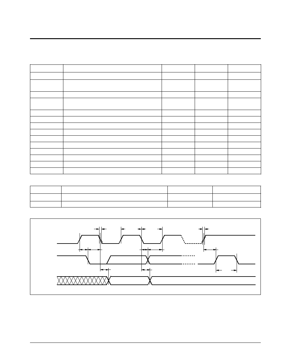
A.C. CHARACTERISTICS (Over recommended operating conditions, unless otherwise specified)
Read & Write Cycle Limits
Symbol
Parameter
Min.
Max.
Units
f
SCL
SCL Clock Frequency
0
100
KHz
T
I
Noise Suppression Time
100
ns
Constant at SCL, SDA Inputs
t
AA
SCL Low to SDA Data Out Valid
0.3
3.5
µs
t
BUF
Time the Bus Must Be Free Before a
4.7
µs
New Transmission Can Start
t
HD:STA
Start Condition Hold Time
4.0
µs
t
LOW
Clock Low Period
4.7
µs
t
HIGH
Clock High Period
4.0
µs
t
SU:STA
Start Condition Setup Time
4.7
µs
t
HD:DAT
Data In Hold Time
0
µs
t
SU:DAT
Data In Setup Time
250
ns
t
R
SDA and SCL Rise Time
1
µs
t
F
SDA and SCL Fall Time
300
ns
t
SU:STO
Stop Condition Setup Time
4.7
µs
t
DH
Data Out Hold Time
300
ns
3837 PGM T06
POWER-UP TIMING
Symbol
Parameter
Max.
Units
t
PUR
(4)
Power-up to Read Operation
1
ms
t
PUW
(4)
Power-up to Write Operation
5
ms
3837 PGM T07
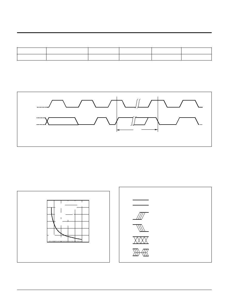
Bus Timing
tSU:STA
tHD:STA
tHD:DAT
tSU:DAT
tLOW
tSU:STO
tR
tBUF
SCL
SDA IN
SDA OUT
tDH
tAA
tF
tHIGH
3837 FHD F04
Note:
(4) t
PUR
and t
PUW
are the delays required from the time V
CC
is stable until the specified operation can be initiated. These parameters
are periodically sampled and not 100% tested.
10
X24C01
WRITE CYCLE LIMITS
Symbol
Parameter
Min.
Typ.
(5)
Max.
Units
t
WR
(6)
Write Cycle Time
5
10
ms
3837 PGM T08
The write cycle time is the time from a valid stop
condition of a write sequence to the end of the internal
erase/program cycle. During the write cycle, the X24C01
Write Cycle Timing
bus interface circuits are disabled, SDA is allowed to
remain high, and the device does not respond to its word
address.
SDA
8th BIT
WORD n
ACK
tWR
STOP
CONDITION
START
CONDITION
X24C01
ADDRESS
SCL
3837 FHD F05
Guidelines for Calculating Typical Values of
Bus Pull-Up Resistors
SYMBOL TABLE
Must be
steady
Will be
steady
May change
from Low to
High
Will change
from Low to
High
May change
from High to
Low
Will change
from High to
Low
Don't Care:
Changes
Allowed
Changing:
State Not
Known
N/A
Center Line
is High
Impedance
OUTPUTS
INPUTS
WAVEFORM
3837 FHD F15
120
100
80
40
60
20
20
40
60
80 100 120
0
0
RESIST
ANCE (K
)
BUS CAPACITANCE (pF)
MIN.
RESISTANCE
MAX.
RESISTANCE
RMAX =
CBUS
tR
RMIN =
IOL MIN
VCC MAX
=2.6K
Notes: (5) Typical values are for T
A
= 25∞C and nominal supply voltage (5V).
(6) t
WR
is the minimum cycle time to be allowed from the system perspective unless polling techniques are used. It is the maximum
time the device requires to automatically complete the internal write operation.
X24C01
11
0.020 (0.51)
0.016 (0.41)
0.150 (3.81)
0.125 (3.18)
0.325 (8.25)
0.300 (7.62)
0.110 (2.79)
0.090 (2.29)
0.430 (10.92)
0.360 (9.14)
0.300
(7.62) REF.
PIN 1 INDEX
0.140 (3.56)
0.130 (3.30)
0.020 (0.51)
0.015 (0.38)
PIN 1
SEATING
PLANE
0.062 (1.57)
0.058 (1.47)
0.255 (6.47)
0.245 (6.22)
0.060 (1.52)
0.020 (0.51)
TYP. 0.010 (0.25)
0
∞
15
∞
0.092 (2.34)
DIA. NOM.
HALF SHOULDER WIDTH ON
ALL END PINS OPTIONAL
0.015 (0.38)
MAX.
PACKAGING INFORMATION
8-LEAD PLASTIC IN-LINE PACKAGE TYPE P
NOTE: ALL DIMENSIONS IN INCHES (IN PARENTHESES IN MILLIMETERS)
12
X24C01
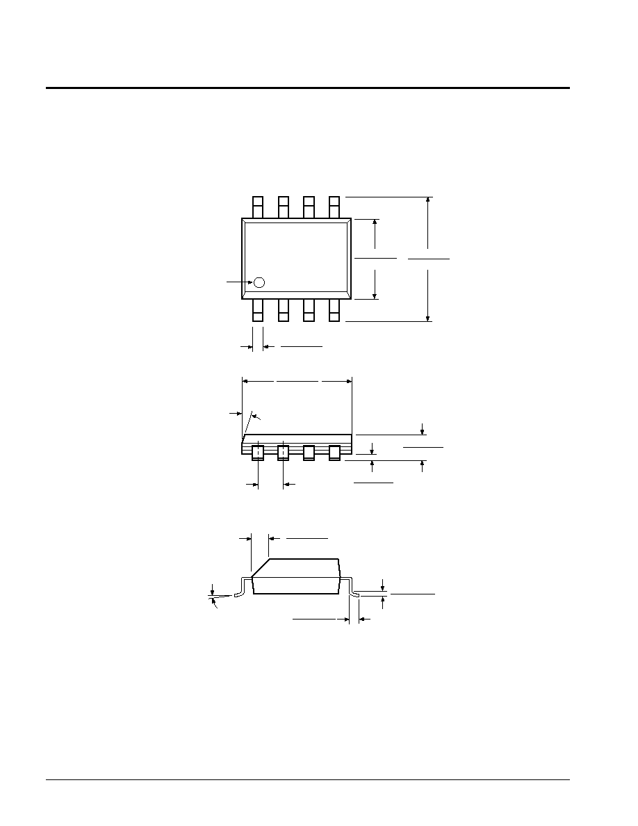
PACKAGING INFORMATION
0.150 (3.80)
0.158 (4.00)
0.228 (5.80)
0.244 (6.20)
0.014 (0.35)
0.019 (0.49)
PIN 1
PIN 1 INDEX
0.010 (0.25)
0.020 (0.50)
0.050 (1.27)
0.188 (4.78)
0.197 (5.00)
0.004 (0.19)
0.010 (0.25)
0.053 (1.35)
0.069 (1.75)
(4X) 7
∞
0.027 (0.683)
0.037 (0.937)
0.0075 (0.19)
0.010 (0.25)
0
∞
≠ 8
∞
X 45
∞
3926 FHD F22
8-LEAD PLASTIC SMALL OUTLINE GULL WING PACKAGE TYPE S
NOTE: ALL DIMENSIONS IN INCHES (IN PARENTHESIS IN MILLIMETERS)
X24C01
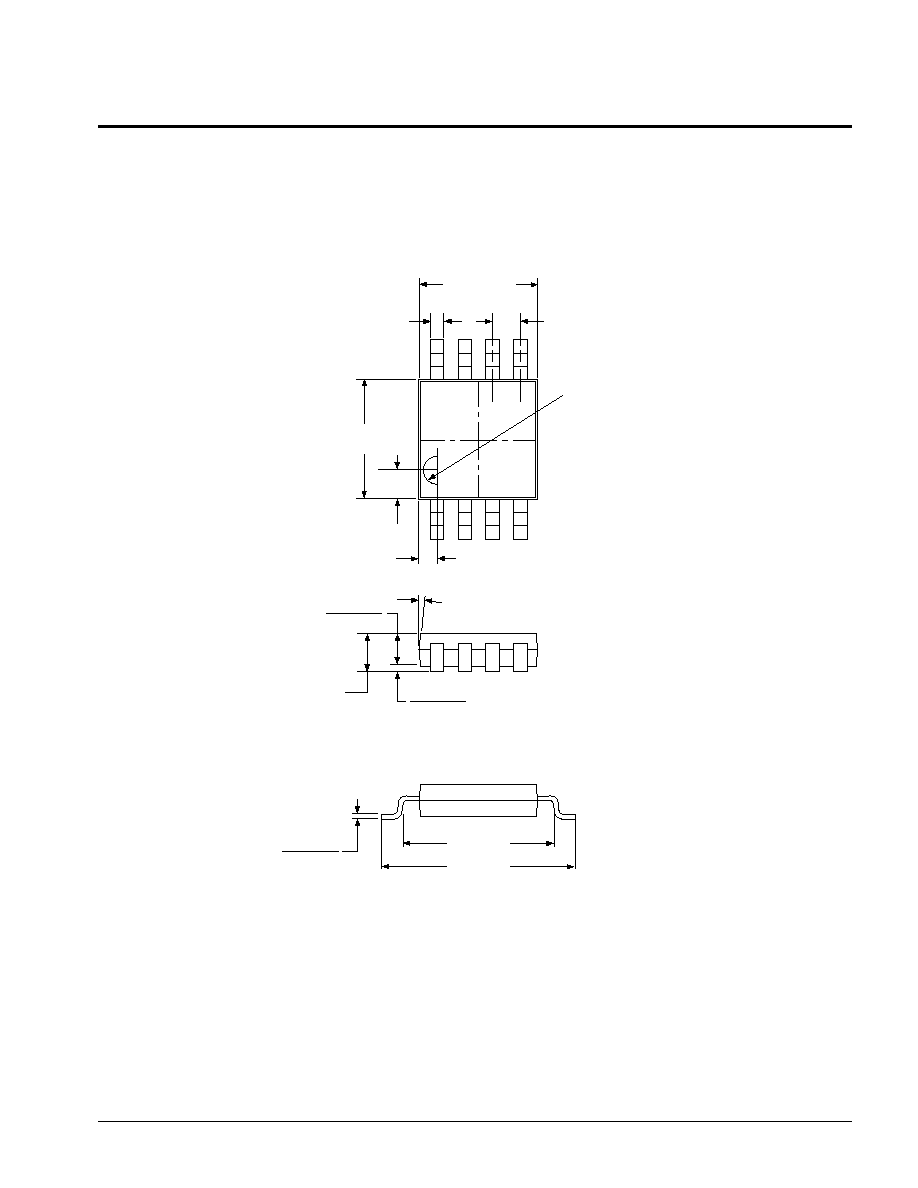
13
0.118
±
0.002
(3.00
±
0.05)
0.040
±
0.002
(1.02
±
0.05)
0.150 (3.81)
REF.
0.193 (4.90)
REF.
0.030 (0.76)
0.036 (0.91)
0.032 (0.81)
0.007 (0.18)
0.005 (0.13)
0.008 (0.20)
0.004 (0.10)
0.0216 (0.55)
7
∞
TYP
R 0.014 (0.36)
0.118
±
0.002
(3.00
±
0.05)
0.012 + 0.006 / -0.002
(0.30 + 0.15 / -0.05)
0.0256 (0.65) TYP
8-LEAD MINIATURE SMALL OUTLINE GULL WING PACKAGE TYPE M
NOTE:
1. ALL DIMENSIONS IN INCHES AND (MILLIMETERS)
3003 ILL 01
PACKAGING INFORMATION

14
X24C01
LIMITED WARRANTY
Devices sold by Xicor, Inc. are covered by the warranty and patent indemnification provisions appearing in its Terms of Sale only. Xicor, Inc. makes no warranty,
express, statutory, implied, or by description regarding the information set forth herein or regarding the freedom of the described devices from patent infringement.
Xicor, Inc. makes no warranty of merchantability or fitness for any purpose. Xicor, Inc. reserves the right to discontinue production and change specifications and
prices at any time and without notice.
Xicor, Inc. assumes no responsibility for the use of any circuitry other than circuitry embodied in a Xicor, Inc. product. No other circuits, patents, licenses are
implied.
U.S. PATENTS
Xicor products are covered by one or more of the following U.S. Patents: 4,263,664; 4,274,012; 4,300,212; 4,314,265; 4,326,134; 4,393,481; 4,404,475;
4,450,402; 4,486,769; 4,488,060; 4,520,461; 4,533,846; 4,599,706; 4,617,652; 4,668,932; 4,752,912; 4,829, 482; 4,874, 967; 4,883, 976. Foreign patents and
additional patents pending.
LIFE RELATED POLICY
In situations where semiconductor component failure may endanger life, system designers using this product should design the system with appropriate error
detection and correction, redundancy and back-up features to prevent such an occurence.
Xicor's products are not authorized for use in critical components in life support devices or systems.
1. Life support devices or systems are devices or systems which, (a) are intended for surgical implant into the body, or (b) support or sustain life, and whose
failure to perform, when properly used in accordance with instructions for use provided in the labeling, can be reasonably expected to result in a significant
injury to the user.
2. A critical component is any component of a life support device or system whose failure to perform can be reasonably expected to cause the failure of the life
support device or system, or to affect its safety or effectiveness.
Device
ORDERING INFORMATION
V
CC
Limits
Blank = 4.5V to 5.5V
3.5 = 3.5V to 5.5V
3 = 3.0V to 5.5V
2.7 = 2.7V to 5.5V
Temperature Range
Blank = Commercial = 0∞C to +70∞C
I = Industrial = ≠40∞C to +85∞C
M = Military = ≠55∞C to +125∞C
Package
P = 8-Lead Plastic DIP
S = 8-Lead SOIC
M = 8-Lead MSOP
X24C01 X X
-X
X24C01 X
X
Blank = 8-Lead SOIC
P = 8-Lead Plastic DIP
M = 8-Lead MSOP
Blank = 4.5V to 5.5V, 0∞C to +70∞C
F = 2.7V to 5.5V, 0∞C to +70∞C
G = 2.7V to 5.5V, ≠40∞C to +85∞C
I = 4.5V to 5.5V, ≠40∞C to +85∞C
B = 3.5V to 5.5V, 0∞C to +70∞C
C = 3.5V to 5.5V, ≠40∞C to +85∞C
D = 3.0V to 5.5V, 0∞C to +70∞C
E = 3.0V to 5.5V, ≠40∞C to +85∞C
M = 4.5V to 5.5V, ≠55∞C to +125∞C
Part Mark Convention