 | –≠–ª–µ–∫—Ç—Ä–æ–Ω–Ω—ã–π –∫–æ–º–ø–æ–Ω–µ–Ω—Ç: X24C44SM | –°–∫–∞—á–∞—Ç—å:  PDF PDF  ZIP ZIP |
Document Outline
- Table of Contents
- Product Selection
- Data Sheet Alpha
- Ap Note Alpha
X24C44
1
Serial Nonvolatile Static RAM
© Xicor, Inc. 1991, 1995, 1996 Patents Pending
Characteristics subject to change without notice
3832-1.5 6/19/96 T2/C1/D1 NS
FEATURES
∑
Advanced CMOS Version of Xicor's X2444
∑
16 x 16 Organization
∑
Single 5 Volt Supply
∑
Ideal for use with Single Chip Microcomputers
--Static Timing
--Minimum I/O Interface
--Serial Port Compatible (COPSTM, 8051)
--Easily Interfaced to Microcontroller Ports
∑
Software and Hardware Control of Nonvolatile
Functions
∑
Auto Recall on Power-Up
∑
TTL and CMOS Compatible
∑
Low Power Dissipation
--Active Current: 10mA Maximum
--Standby Current: 50
µ
A Maximum
∑
8-Lead PDIP, Cerdip, and 8-Lead SOIC Packages
∑
High Reliability
--Store Cycles: 1,000,000
--Data Retention: 100 Years
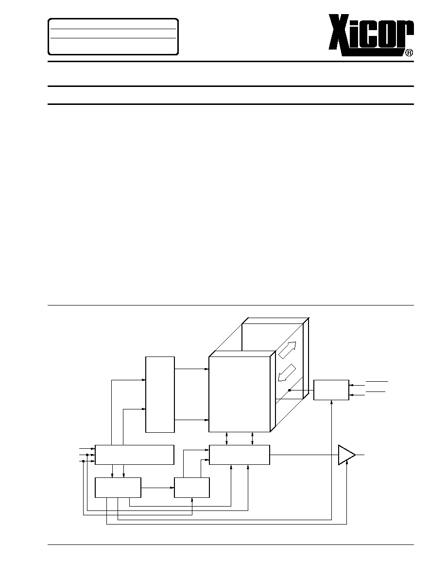
FUNCTIONAL DIAGRAM
256 Bit
X24C44
16 x 16 Bit
NONVOLATILE
E
2
PROM
CONTROL
LOGIC
COLUMN
DECODE
ROW
DECODE
4-BIT
COUNTER
INSTRUCTION
DECODE
INSTRUCTION
REGISTER
CE (1)
DI (3)
SK (2)
DO (4)
RECALL (6)
STORE (7)
STATIC
RAM
256-BIT
RECALL
ST
ORE
3832 FHD F01
DESCRIPTION
The Xicor X24C44 is a serial 256 bit NOVRAM featuring
a static RAM configured 16 x 16, overlaid bit-by-bit with
a nonvolatile E
2
PROM array. The X24C44 is fabricated
with Xicor's Advanced CMOS Floating Gate technology.
The Xicor NOVRAM design allows data to be transferred
between the two memory arrays by means of software
commands or external hardware inputs. A store opera-
tion (RAM data to E
2
PROM) is completed in 5ms or less
and a recall operation (E
2
PROM data to RAM) is com-
pleted in 2
µ
s or less.
Xicor NOVRAMs are designed for unlimited write opera-
tions to RAM, either from the host or recalls from
E
2
PROM and a minimum 1,000,000 store operations.
Inherent data retention is specified to be greater than
100 years.
COPS is a trademark of National Semiconductor Corp.
A
PPLICATION
N
OTES
A V A I L A B L E
AN3 ∑ AN7 ∑ AN8 ∑ AN15 ∑ AN16 ∑ AN25 ∑ AN29
∑ AN30 ∑ AN35 ∑ AN36 ∑ AN39 ∑ AN56 ∑ AN69

2
X24C44
PIN CONFIGURATION
PIN DESCRIPTIONS
Chip Enable (CE)
The Chip Enable input must be HIGH to enable all read/
write operations. CE must remain HIGH following a
Read or Write command until the data transfer is com-
plete. CE LOW places the X24C44 in the low power
standby mode and resets the instruction register. There-
fore, CE must be brought LOW after the completion of an
operation in order to reset the instruction register in
preparation for the next command.
Serial Clock (SK)
The Serial Clock input is used to clock all data into and
out of the device.
Data In (DI)
Data In is the serial data input.
Data Out (DO)
Data Out is the serial data output. It is in the high
impedance state except during data output cycles in
response to a READ instruction.
STORE
STORE
LOW will initiate an internal transfer of data from
RAM to the E
2
PROM array.
RECALL
RECALL
LOW will initiate an internal transfer of data
from E
2
PROM to the RAM array.
PIN NAMES
Symbol
Description
CE
Chip Enable
SK
Serial Clock
DI
Serial Data In
DO
Serial Data Out
RECALL
Recall Input
STORE
Store Input
V
CC
+5V
V
SS
Ground
3832 PGM T01
3832 FHD F02.2
CE
SK
DI
DO
1
2
3
4
8
7
6
5
VCC
STORE
RECALL
VSS
X24C44
PDIP/CERDIP/SOIC

X24C44
3
DEVICE OPERATION
The X24C44 contains an 8-bit instruction register. It is
accessed via the DI input, with data being clocked in on
the rising edge of SK. CE must be HIGH during the entire
data transfer operation.
Table 1. contains a list of the instructions and their
operation codes. The most significant bit (MSB) of all
instructions is a logic one (HIGH), bits 6 through 3 are
either RAM address bits (A) or don't cares (X) and bits
2 through 0 are the operation codes. The X24C44
requires the instruction to be shifted in with the MSB first.
After CE is HIGH, the X24C44 will not begin to interpret
the data stream until a logic "1" has been shifted in on DI.
Therefore, CE may be brought HIGH with SK running
and DI LOW. DI must then go HIGH to indicate the start
condition of an instruction before the X24C44 will begin
any action.
In addition, the SK clock is totally static. The user can
completely stop the clock and data shifting will be stopped.
Restarting the clock will resume shifting of data.
RCL and
RECALL
Either a software RCL instruction or a LOW on the
RECALL
input will initiate a transfer of E
2
PROM data
into RAM. This software or hardware recall operation
sets an internal "previous recall" latch. This latch is reset
upon power-up and must be intentionally set by the user
to enable any write or store operations. Although a recall
operation is performed upon power-up, the previous
recall latch is not set by this operation.
WRDS and WREN
Internally the X24C44 contains a "write enable" latch. This
latch must be set for either writes to the RAM or store
operations to the E
2
PROM. The WREN instruction sets
the latch and the WRDS instruction resets the latch,
disabling both RAM writes and E
2
PROM stores, effec-
tively protecting the nonvolatile data from corruption. The
write enable latch is automatically reset on power-up.
STO and
STORE
Either the software STO instruction or a LOW on the
STORE
input will initiate a transfer of data from RAM to
E
2
PROM. In order to safeguard against unwanted store
operations, the following conditions must be true:
∑ STO instruction issued or
STORE
input is LOW.
∑ The internal "write enable" latch must be set
(WREN instruction issued).
∑ The "previous recall" latch must be set (either a
software or hardware recall operation).
Once the store cycle is initiated, all other device func-
tions are inhibited. Upon completion of the store cycle,
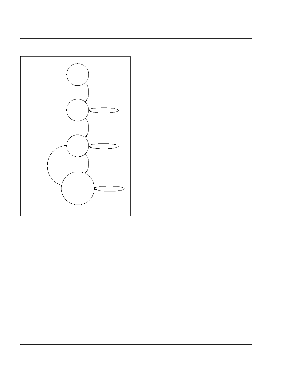
the write enable latch is reset. Refer to Figure 4 for a
state diagram description of enabling/disabling condi-
tions for store operations.
WRITE
The WRITE instruction contains the 4-bit address of the
word to be written. The write instruction is immediately
followed by the 16-bit word to be written. CE must remain
HIGH during the entire operation. CE must go LOW
before the next rising edge of SK. If CE is brought LOW
prematurely (after the instruction but before 16 bits of data
are transferred), the instruction register will be reset and
the data that was shifted-in will be written to RAM.
If CE is kept HIGH for more than 24 SK clock cycles (8-bit
instruction plus 16-bit data), the data already shifted-in will
be overwritten.
Table 1. Instruction Set
Instruction
Format, I
2
I
1
I
0
Operation
WRDS (Figure 3)
1XXXX000
Reset Write Enable Latch (Disables Writes and Stores)
STO (Figure 3)
1XXXX001
Store RAM Data in E
2
PROM
Reserved
1XXXX010
N/A
WRITE (Figure 2)
1AAAA011
Write Data into RAM Address AAAA
WREN (Figure 3)
1XXXX100
Set Write Enable Latch (Enables Writes and Stores)
RCL (Figure 3)
1XXXX101
Recall E
2
PROM Data into RAM
READ (Figure 1)
1AAAA11X
Read Data from RAM Address AAAA
3832 PGM T13
X = Don't Care
A = Address

4
X24C44
READ
The READ instruction contains the 4-bit address of the
word to be accessed. Unlike the other six instructions, I
0
of the instruction word is a "don't care". This provides two
advantages. In a design that ties both DI and DO
together, the absence of an eighth bit in the instruction
allows the host time to convert an I/O line from an output
to an input. Secondly, it allows for valid data output
during the ninth SK clock cycle.
D0, the first bit output during a read operation, is trun-
cated. That is, it is internally clocked by the falling edge
of the eighth SK clock; whereas, all succeeding bits are
clocked by the rising edge of SK (refer to Read Cycle
Diagram).
LOW POWER MODE
When CE is LOW, non-critical internal devices are
powered-down, placing the device in the standby power
mode, thereby minimizing power consumption.
SLEEP
Because the X24C44 is a low power CMOS device, the
SLEEP instruction implemented on the first generation
NMOS device has been deleted. For systems convert-
ing from the X2444 to the X24C44 the software need not
be changed; the instruction will be ignored.
WRITE PROTECTION
The X24C44 provides two software write protection
mechanisms to prevent inadvertent stores of unknown
data.
Power-Up Condition
Upon power-up the "write enable" latch is in the reset
state, disabling any store operation.
Unknown Data Store
The "previous recall" latch must be set after power-up.
It may be set only by performing a software or hardware
recall operation, which assures that data in all RAM
locations is valid.
SYSTEM CONSIDERATIONS
Power-Up Recall
The X24C44 performs a power-up recall that transfers
the E
2
PROM contents to the RAM array. Although the
data may be read from the RAM array, this recall does
not set the "previous recall" latch. During this power-up
recall operation, all commands are ignored. Therefore,
the host should delay any operations with the X24C44 a
minimum of t
PUR
after V
CC
is stable.
Power-Down Data Protection
Because the X24C44 is a 5V only nonvolatile memory
device it may be susceptible to inadvertent stores to the
E
2
PROM array during power-down cycles. Power-up
cycles are not a problem because the "previous recall"
latch and "write enable" latch are reset, preventing any
possible corruption of E
2
PROM data.
Software Power-Down Protection
If the
STORE
and
RECALL
pins are tied to V
CC
through
a pull-up resistor and only software operations are
performed to initiate stores, there is little likelihood of an
inadvertent store. However, if these two lines are under
microprocessor control, positive action should be em-
ployed to negate the possibility of these control lines
bouncing and generating an unwanted store. The safest
method is to issue the WRDS command after a write
sequence and also following store operations. Note: an
internal store may take up to 5ms; therefore, the host
microprocessor should delay 5ms after initiating the
store prior to issuing the WRDS command.
Hardware Power-Down Protection
(when the "write enable" latch and "previous recall" latch
are not in the reset state):
Holding either
RECALL
LOW, CE LOW or
STORE
HIGH during power-down will prevent an inadvertent
store.

X24C44
5
Figure 1. RAM Read
3832 FHD F07.1
Figure 2. RAM Write
3832 FHD F08.1
Figure 3. Non-Data Operations
3832 FHD F09.1
1
CE
2
3
4
5
6
7
8
1
A
1
A
A
A
1
SK
DI
9
10
11
21
22
23
24
D0
D1
D2
D12
D13
D14
D15
0
1
CE
2
3
4
5
6
7
8
1
X
I
2
X
X
X
I
1
I
0
SK
DI
1
CE
2
3
4
5
6
7
8
1
A
1
A
A
A
1
X*
SK
DI
9
10
11
12
22
23
24
D1
D2
D3
D14
D15
D0
D13
DO
HIGH Z
*Bit 8 of Read Instructions is Don't Care
D0
6
X24C44
Figure 4. X24C44 State Diagram
POWER
ON
STORE
ENABLED
RAM READ
OR WRITE
RAM
READ
ENABLED
RAM
READ
ENABLED
RAM
READ &
WRITE
WREN
COMMAND
RAM READ
RAM READ
POWER-UP
RECALL
RCL COMMAND
OR RECALL
STO OR
WRDS CMD
OR STORE
3832 FHD F10.1

X24C44
7
ABSOLUTE MAXIMUM RATINGS*
Temperature under Bias .................. ≠65
∞
C to +135
∞
C
Storage Temperature ....................... ≠65
∞
C to +150
∞
C
Voltage on any Pin with
Respect to V
SS ............................................
≠1V to +7V
D.C. Output Current ............................................. 5mA
Lead Temperature
(Soldering, 10 seconds) .............................. 300
∞
C
*COMMENT
Stresses above those listed under "Absolute Maximum
Ratings" may cause permanent damage to the device.
This is a stress rating only and the functional operation of
the device at these or any other conditions above those
indicated in the operational sections of this specification is
not implied. Exposure to absolute maximum rating condi-
tions for extended periods may affect device reliability.
CAPACITANCE T
A
= +25
∞
C, f = 1MHz, V
CC
= 5V
Symbol
Parameter
Max.
Units
Test Conditions
C
OUT
(2)
Output Capacitance
8
pF
V
OUT
= 0V
C
IN
(2)
Input Capacitance
6
pF
V
IN
= 0V
3832 PGM T06.1
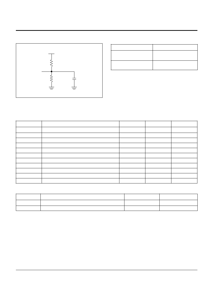
RECOMMENDED OPERATING CONDITIONS
Temperature
Min.
Max.
Commercial
0
∞
C
+70
∞
C
Industrial
≠40
∞
C
+85
∞
C
Military
≠55
∞
C
+125
∞
C
3832 PGM T02.1
Supply Voltage
Limits
X24C44
5V
±
10%
3832 PGM T03.1
D.C. OPERATING CHARACTERISTICS (Over recommended operating conditions unless otherwise specified.)
Limits
Symbol
Parameter
Min.
Max.
Units
Test Conditions
l
CC
V
CC
Supply Current
10
mA
SK = 0.4V/2.4V Levels @ 1MHz,
(TTL Inputs)
DO = Open, All Other Inputs = V
IH
I
SB1
V
CC
Standby Current
1
mA
DO = Open, CE = V
IL
,
(TTL Inputs)
All Other Inputs = V
IH
I
SB2
V
CC
Standby Current
50
µ
A
DO = Open, CE = V
SS
(CMOS Inputs)
All Other Inputs = V
CC
≠ 0.3V
I
LI
Input Load Current
10
µ
A
V
IN
= V
SS
to V
CC
I
LO
Output Leakage Current
10
µ
A
V
OUT
= V
SS
to V
CC
V
lL
(1)
Input LOW Voltage
≠1
0.8
V
V
IH
(1)
Input HIGH Voltage
2
V
CC
+ 1
V
V
OL
Output LOW Voltage
0.4
V
I
OL
= 4.2mA
V
OH
Output HIGH Voltage
2.4
V
I
OH
= ≠2mA
3832 PGM T04.3
ENDURANCE AND DATA RETENTION
Parameter
Min.
Units
Endurance
100,000
Data Changes Per Bit
Store Cycles
1,000,000
Store Cycles
Data Retention
100
Years
3832 PGM T05
Notes: (1) V
IL
min. and V
IH
max. are for reference only and are not tested.
(2) This parameter is periodically sampled and not 100% tested.
8
X24C44
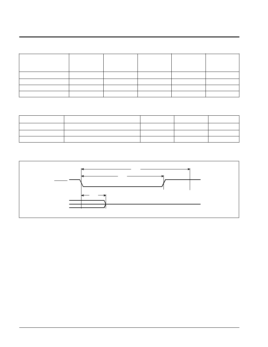
A.C. CONDITIONS OF TEST
Input Pulse Levels
0V to 3V
Input Rise and
Fall Times
10ns
Input and Output
Timing Levels
1.5V
3832 PGM T07.1
EQUIVALENT A.C. LOAD CIRCUIT
A.C. CHARACTERISTICS (Over the recommended operating conditions unless otherwise specified.)
Read and Write Cycle Limits
Symbol
Parameter
Min.
Max.
Units
F
SK
(3)
SK Frequency
1
MHz
t
SKH
SK Positive Pulse Width
400
ns
t
SKL
SK Negative Pulse Width
400
ns
t
DS
Data Setup Time
400
ns
t
DH
Data Hold Time
80
ns
t
PD1
SK to Data Bit 0 Valid
375
ns
t
PD
SK to Data Valid
375
ns
t
Z
Chip Enable to Output High Z
1
µ
s
t
CES
Chip Enable Setup
800
ns
t
CEH
Chip Enable Hold
350
ns
t
CDS
Chip Deselect
800
ns
3832 PGM T08.1
POWER-UP TIMING
Symbol
Parameter
Max.
Units
t
PUR
(4)
Power-up to Read Operation
200
µ
s
t
PUW
(4)
Power-up to Write or Store Operation
5
ms
3832 PGM T09
Notes: (3) SK rise and fall times must be less than 50ns.
(4) t
PUR
and t
PUW
are the delays required from the time V
CC
is stable until the specified operation can be initiated. These parameters
are periodically sampled and not 100% tested.
5V
919
497
OUTPUT
100pF
3832 FHD F11

X24C44
9
Write Cycle
3832 FHD F03
Read Cycle
3832 FHD F04
SK
1/FSK
tCES
tCEH
tCDS
x
1
2
n
tSKH
tSKL
tDS
tDH
CE
DI
SK CYCLE #
SK
6
7
8
9
10
n
D0
D1
Dn
HIGH Z
HIGH Z
CE
DI
DO
DON'T CARE
SK CYCLE #
I2
I1
tPD1
tPD
tZ
VIH
10
X24C44
NONVOLATILE OPERATIONS
Previous
Software
Write Enable
Recall Latch
Operation
STORE
RECALL
Instruction
Latch State
State
Hardware Recall
1
0
NOP
(5)
X
X
Software Recall
1
1
RCL
X
X
Hardware Store
0
1
NOP
(5)
SET
SET
Software Store
1
1
STO
SET
SET
3832 PGM T10
ARRAY RECALL LIMITS
Symbol
Parameter
Min.
Max.
Units
t
RCC
Recall Cycle Time
2
µ
s
t
RCP
Recall Pulse Width
(6)
500
ns
t
RCZ
Recall to Output in High Z
500
ns
3832 PGM T11
Recall Timing
Notes: (5) NOP designates when the X24C44 is not currently executing an instruction.
(6) Recall rise time must be <10
µ
s.
3832 FHD F05
tRCC
tRCP
tRCZ
HIGH Z
RECALL
DO

X24C44
11
STORE CYCLE LIMITS
Symbol
Parameter
Min.
Typ.
(7)
Max.
Units
t
ST
Store Time
2
5
ms
t
STP
Store Pulse Width
200
ns
t
Z
CE to Output in High Z
1
µ
s
V
CC
Store Inhibit
3
V
3832 PGM T12
Store Timing
3832 FHD F06
Note:
(7) Typical values are for T
A
= 25
∞
C and nominal supply voltage.
SYMBOL TABLE
tST
tSTP
tZ
HIGH Z
STORE
DO
CE
WAVEFORM
INPUTS
OUTPUTS
Must be
steady
Will be
steady
May change
from LOW
to HIGH
Will change
from LOW
to HIGH
May change
from HIGH
to LOW
Will change
from HIGH
to LOW
Don't Care:
Changes
Allowed
Changing:
State Not
Known
N/A
Center Line
is High
Impedance
12
X24C44
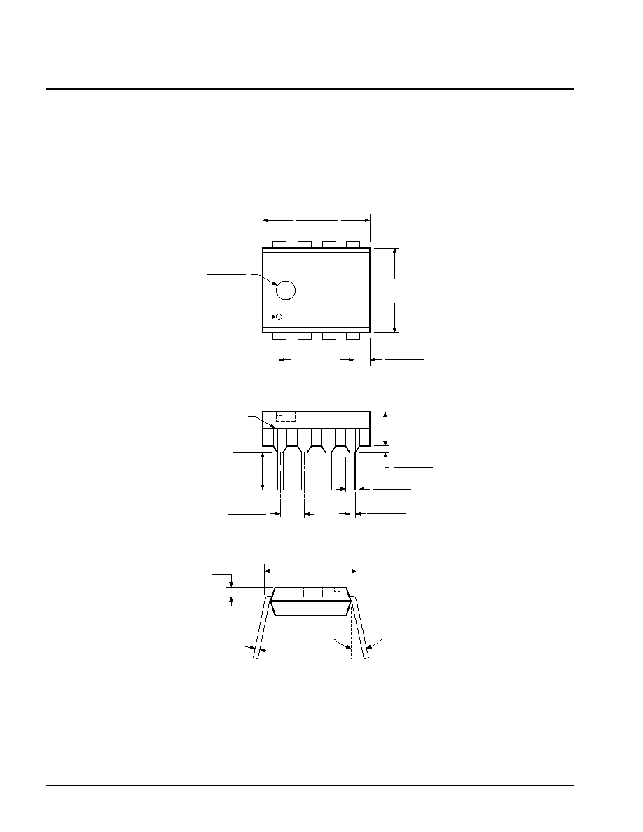
PACKAGING INFORMATION
0.020 (0.51)
0.016 (0.41)
0.150 (3.81)
0.125 (3.18)
0.325 (8.25)
0.300 (7.62)
0.110 (2.79)
0.090 (2.29)
0.430 (10.92)
0.360 (9.14)
0.300
(7.62) REF.
PIN 1 INDEX
0.140 (3.56)
0.130 (3.30)
0.020 (0.51)
0.015 (0.38)
3926 FHD F01
PIN 1
SEATING
PLANE
0.062 (1.57)
0.058 (1.47)
0.255 (6.47)
0.245 (6.22)
0.060 (1.52)
0.020 (0.51)
TYP. 0.010 (0.25)
0
∞
15
∞
8-LEAD PLASTIC DUAL IN-LINE PACKAGE TYPE P
NOTE: ALL DIMENSIONS IN INCHES (IN PARENTHESES IN MILLIMETERS)
0.092 (2.34)
DIA. NOM.
HALF SHOULDER WIDTH ON
ALL END PINS OPTIONAL
0.015 (0.38)
MAX.
X24C44
13
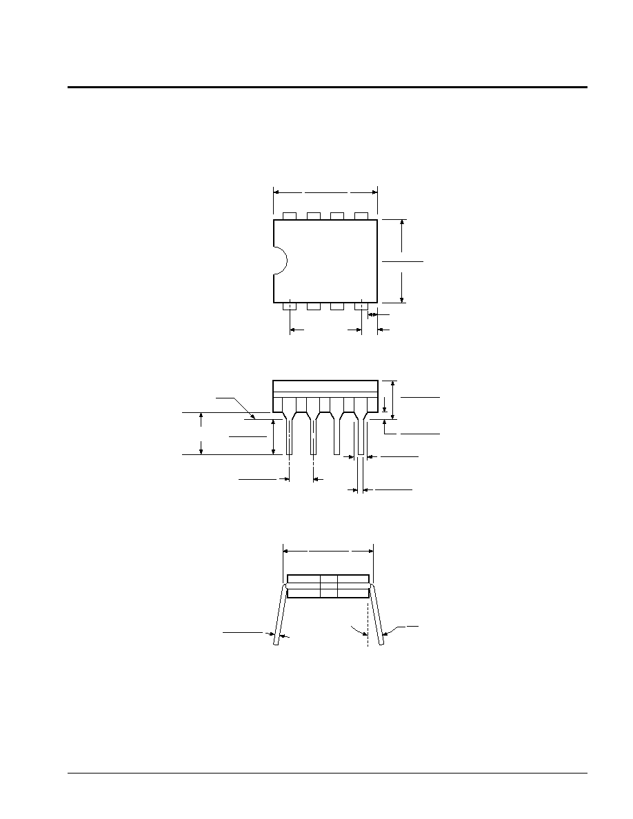
PACKAGING INFORMATION
0.320 (8.13)
0.290 (7.37)
TYP. 0.311 (7.90)
0.110 (2.79)
0.090 (2.29)
TYP. 0.100 (2.54)
0.300 (7.62)
REF.
0.023 (0.58)
0.014 (0.36)
TYP. 0.017 (0.43)
0.200 (5.08)
0.140 (3.56)
0.060 (1.52)
0.015 (0.38)
3926 FHD F05
PIN 1
SEATING
PLANE
0.200 (5.08)
0.125 (3.18)
0.065 (1.65)
0.038 (0.97)
TYP. 0.060 (1.52)
0.310 (7.87)
0.220 (5.59)
0.055 (1.40) MAX.
0
∞
15
∞
8-LEAD HERMETIC DUAL IN-LINE PACKAGE TYPE D
NOTE: ALL DIMENSIONS IN INCHES (IN PARENTHESES IN MILLIMETERS)
0.005 (0.13) MIN.
0.015 (0.38)
0.008 (0.20)
0.405 (10.29)
≠≠
0.150 (3.81) MIN.
14
X24C44
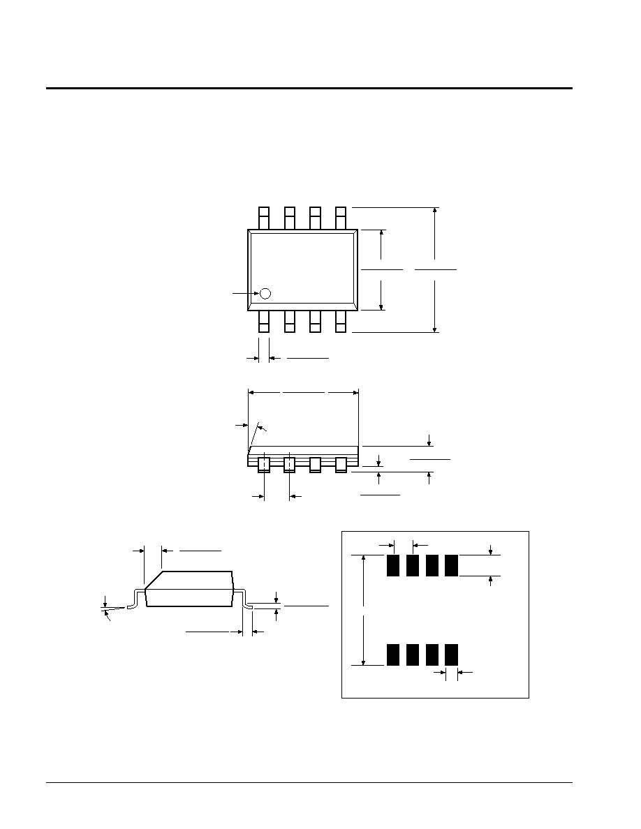
PACKAGING INFORMATION
0.150 (3.80)
0.158 (4.00)
0.228 (5.80)
0.244 (6.20)
0.014 (0.35)
0.019 (0.49)
PIN 1
PIN 1 INDEX
0.010 (0.25)
0.020 (0.50)
0.050 (1.27)
0.188 (4.78)
0.197 (5.00)
0.004 (0.19)
0.010 (0.25)
0.053 (1.35)
0.069 (1.75)
(4X) 7
∞
0.016 (0.410)
0.037 (0.937)
0.0075 (0.19)
0.010 (0.25)
0
∞
≠ 8
∞
X 45
∞
3926 FHD F22.1
8-LEAD PLASTIC SMALL OUTLINE GULL WING PACKAGE TYPE S
NOTE: ALL DIMENSIONS IN INCHES (IN PARENTHESES IN MILLIMETERS)
0.250"
0.050" TYPICAL
0.050"
TYPICAL
0.030"
TYPICAL
8 PLACES
FOOTPRINT
X24C44
15
LIMITED WARRANTY
Devices sold by Xicor, Inc. are covered by the warranty and patent indemnification provisions appearing in its Terms of Sale only. Xicor, Inc. makes
no warranty, express, statutory, implied, or by description regarding the information set forth herein or regarding the freedom of the described
devices from patent infringement. Xicor, Inc. makes no warranty of merchantability or fitness tor any purpose. Xicor, Inc. reserves the right to
discontinue production and change specifications and prices at any time and without notice.
Xicor, Inc. assumes no responsibility for the use of any circuitry other than circuitry embodied in a Xicor, Inc. product. No other circuits, patents,
licenses are implied.
US. PATENTS
Xicor products are covered by one or more of the following U.S. Patents: 4,263,664; 4,274,012; 4,300,212; 4,314,265; 4,326,134; 4,393,481;
4,404,475; 4,450,402; 4,486,769; 4,488,060; 4,520,461; 4,533,846; 4,599,706; 4,617,652; 4,668,932; 4,752,912; 4,829,482; 4,874,967;
4,883,976. Foreign patents and additional patents pending.
LIFE RELATED POLICY
In situations where semiconductor component failure may endanger life, system designers using this product should design the system with
appropriate error detection and correction, redundancy and back-up features to prevent such an occurrence.
Xicor's products are not authorized for use as critical components in life support devices or systems.
1. Life support devices or systems are devices or systems which, (a) are intended for surgical implant into the body, or (b) support or sustain life,
and whose failure to perform, when properly used in accordance with instructions for use provided in the labeling, can be reasonably expected
to result in a significant injury to the user.
2. A critical component is any component of a life support device or system whose failure to perform can be reasonably expected to cause the failure
of the life support device or system, or to affect its satety or effectiveness.
ORDERING INFORMATION
Device
X24C44
P
T
-V
V
CC
Limits
Blank = 5V
±
10%
Temperature Range
Blank = Commercial = 0
∞
C to +70
∞
C
I = Industrial = ≠40
∞
C to +85
∞
C
M = Military = ≠55
∞
C to +125
∞
C
Package
P = 8-Lead Plastic DIP
D = 8-Lead Ceramic DIP
S = 8-Lead SOIC