Document Outline
- Table of Contents
- Product Selection
- Data Sheet Alpha
- Ap Note Alpha
SerialFlash
TM
Memory with Block Lock
TM
Protection
64K/32K/16K
8K/4K/2K x 8 Bit
©
Xicor, 1995, 1996 Patents Pending
6686-3.8 8/29/96 T3/C0/D0 SH
1
Characteristics subject to change without notice
X24F064/032/016
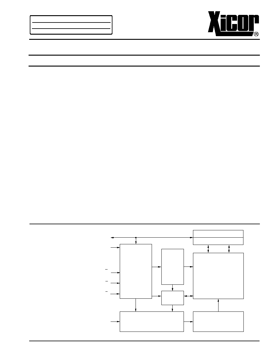
FUNCTIONAL DIAGRAM
FEATURES
∑
1.8V to 3.6V or 5V "Univolt" Read and
Program Power Supply Versions
∑
Low Power CMOS
--Active Read Current Less Than 1mA
--Active Program Current Less Than 3mA
--Standby Current Less Than 1
µ
A
∑
Internally Organized 8K/4K/2K x 8
∑
New Programmable Block Lock Protection
--Software Write Protection
--Programmable hardware Write Protect
∑
Block Lock (0, 1/4, 1/2, or all of the Flash
Memory array)
∑
2 Wire Serial Interface
∑
Bidirectional Data Transfer Protocol
∑
32 Byte Sector Programming
∑
Self Timed Program Cycle
--Typical Programming Time of 5ms
Per Sector
∑
High Reliability
--Endurance: 100,000 cycles per byte
--Data Retention: 100 Years
∑
Available Packages
--8-Lead PDIP
--8-Lead SOIC (JEDEC)
--14-Lead TSSOP (X24F032/016)
--20-Lead TSSOP (X24F064)
DESCRIPTION
The X24F064/032/016 is a CMOS SerialFlash
Memory Family, internally organized 8K/4K/2K x 8.
The family features a serial interface and software
protocol allowing operation on a simple two wire bus.
Device select inputs (S
0
,
S
1
,
S
2
) allow up to eight
devices to share a common two wire bus.
A Program Protect Register accessed at the highest
address location, provides three new programming
protection features: Software Programming Protection,
Block Lock Protection, and Hardware Programming
Protection. The Software Programming Protection
feature prevents any nonvolatile writes to the device
until the WEL bit in the program protect register is set.
The Block Lock
TM
Protection feature allows the user to
individually protect four blocks of the array by program-
ming two bits in the programming protect register. The
Programmable Hardware Program Protect feature
allows the user to install each device with PP tied to
V
CC
, program the entire memory array in place, and
then enable the hardware programming protection by
programming a PPEN bit in the program protect
register. After this, selected blocks of the array,
including the program protect register itself, are
permanently protected from being programmed.
6686 ILL F01.5
COMMAND
DECODE
AND CONTROL
LOGIC
X
DECODE
LOGIC
SECTORED
MEMORY
ARRAY
SDA
SCL
S
2
/S
2
PROGRAM
PROTECT
REGISTER
PROGRAMMING
CONTROL LOGIC
PP
HIGH VOLTAGE
CONTROL
SECTOR DECODE LOGIC
32
8
DATA REGISTER
S
1
/S
1
S
0
/S
0
SerialFlash
TM
Memory and Block Lock
TM
Protection are trademarks of Xicor, Inc.
A
PPLICATION
N
OTE
A V A I L A B L E
AN76 ∑ AN78 ∑ AN81 ∑ AN87
X24F064/032/016
2
Xicor SerialFlash Memories are designed and tested for
applications requiring extended endurance. Inherent
data retention is greater than 100 years.
PIN DESCRIPTIONS
Serial Clock (SCL)
The SCL input is used to clock all data into and out of
the device.
Serial Data (SDA)
SDA is a bidirectional pin used to transfer data into
and out of the device. It is an open drain output and
may be wire-ORed with any number of open drain or
open collector outputs.
An open drain output requires the use of a pull-up
resistor. For selecting typical values, refer to the pull-
up resistor selection graph at the end of this data
sheet.
Device Select (S
0
, S
0
, S
1
, S
1
, S
2
, S
2
)
The device select inputs are used to set the device
select bits of the 8-bit slave address. This allows
multiple devices to share a common bus. These inputs
can be static or actively driven. If used statically they
must be tied to V
SS
or V
CC
as appropriate. If actively
driven, they must be driven with CMOS levels (driven
to V
CC
or V
SS
).
Program Protect (PP)
The program protect input controls the hardware
program protect feature. When held LOW, hardware
program protection is disabled and the X24F064/
032/016 can be programmed normally. When this
input is held HIGH, and the PPEN bit in the
program protect register is set HIGH, program
protection is enabled, and nonvolatile writes are
disabled to the selected blocks as well as the
program protect register itself.
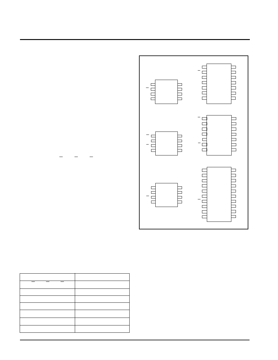
PIN NAMES
6686 FRM T01.1
Symbol
Description
S
0
,
S
0
, S
1
,
S
1
, S
2
,
S
2
Device Select Inputs
SDA
Serial Data
SCL
Serial Clock
PP
Program Protect
V
SS
Ground
V
CC
Supply Voltage
NC
No Connect
PIN CONFIGURATION
S
0
S
1
NC
NC
NC
S
2
VSS
14-LEAD TSSOP
VCC
PP
NC
NC
NC
SCL
SDA
14-LEAD TSSOP
S
0
S
1
NC
NC
NC
S
2
VSS
VCC
PP
NC
NC
NC
SCL
SDA
20-LEAD TSSOP
NC
NC
S
1
NC
NC
NC
S
2
VSS
NC
NC
NC
VCC
PP
NC
NC
NC
SCL
SDA
NC
NC
VCC
PP
SCL
SDA
S0
S1
S2
VSS
1
2
3
4
8
7
6
5
8-LEAD DIP & SOIC
1
2
3
4
5
6
7
14
13
12
11
10
9
8
VCC
PP
SCL
SDA
S0
S1
S2
VSS
1
2
3
4
8
7
6
5
8-LEAD DIP & SOIC
1
2
3
4
5
6
7
14
13
12
11
10
9
8
VCC
PP
SCL
SDA
NC
S
1
S
2
VSS
1
2
3
4
8
7
6
5
8-LEAD DIP & SOIC
1
2
3
4
5
6
7
8
9
10
20
19
18
17
16
15
14
13
12
11
X24F064
X24F032
X24F016
6686 ILL F02.4
X24F064/032/016
3
DEVICE OPERATION
The X24F064/032/016 supports a bidirectional bus ori-
ented protocol. The protocol defines any device that
sends data onto the bus as a transmitter, and the re-
ceiving device as the receiver. The device controlling
the transfer is a master and the device being controlled
is the slave. The master will always initiate data trans-
fers, and provide the clock for both transmit and receive
operations. Therefore, the X24F064/032/016 will be
considered a slave in all applications.
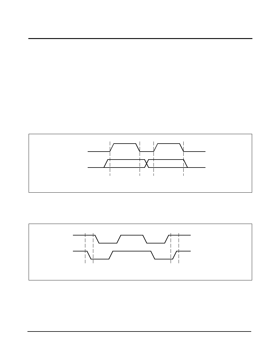
Clock and Data Conventions
Data states on the SDA line can change only during
SCL LOW. SDA state changes during SCL HIGH are
reserved for indicating start and stop conditions. Refer
to Figures 1 and 2.
Start Condition
All commands are preceded by the start condition,
which is a HIGH to LOW transition of SDA when SCL is
HIGH. The X24F064/032/016 continuously monitors
the SDA and SCL lines for the start condition and will
not respond to any command until this condition has
been met.
SCL
SDA
DATA STABLE
DATA
CHANGE
6686 ILL F04
SCL
SDA
START BIT
STOP BIT
6686 ILL F05
Figure 1. Data Validity
Figure 2. Definition of Start and Stop
Notes:
(5) Typical values are for T
A
= 25
∞
C and nominal supply voltage (2.7V)
(6) t
PR
is the minimum cycle time from the system perspective when polling techniques are not used. It is the maximum time the
device requires to perform the internal program operation.
X24F064/032/016
4
Stop Condition
All communications must be terminated by a stop
condition, which is a LOW to HIGH transition of SDA
when SCL is HIGH. The stop condition is also used to
place the device into the standby power mode after a
read sequence. A stop condition can only be issued
after the transmitting device has released the bus.
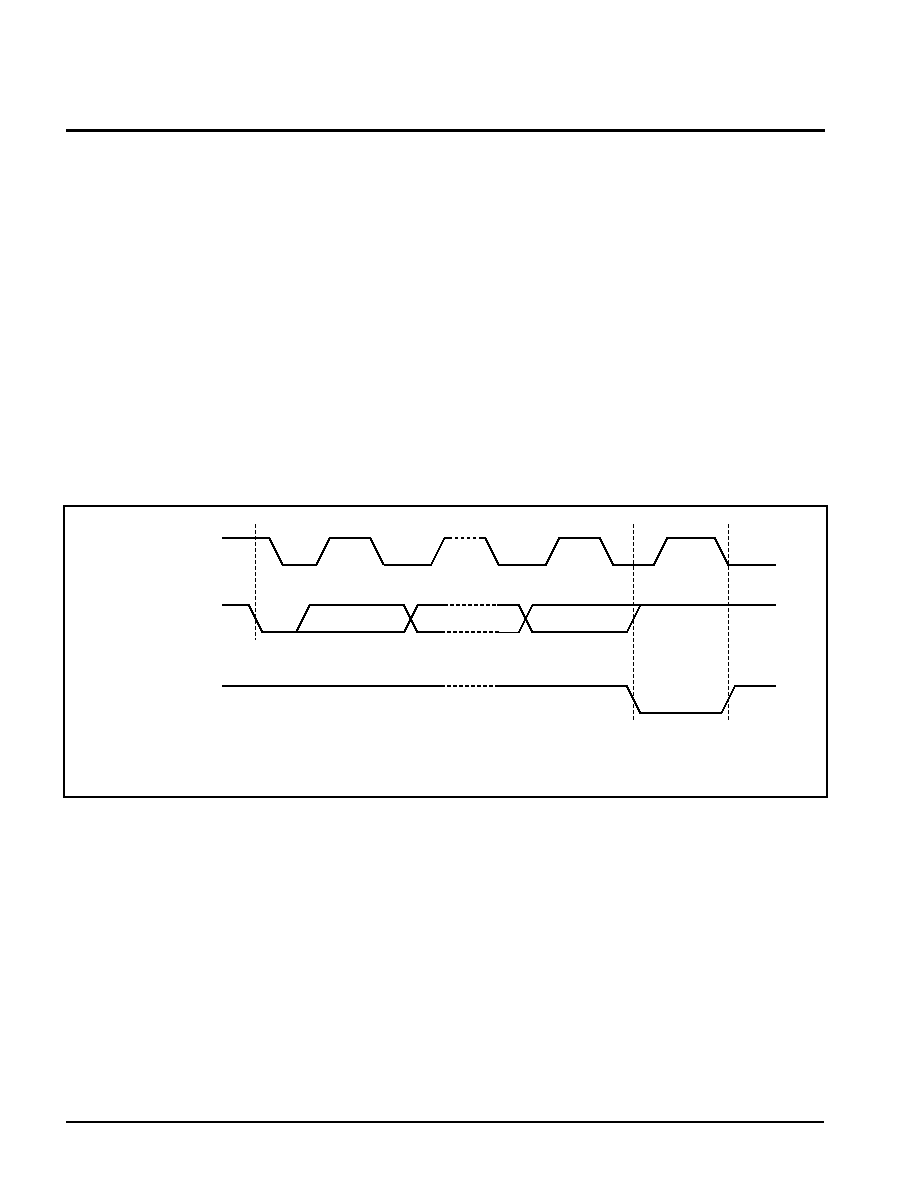
Acknowledge
Acknowledge is a software convention used to indicate
successful data transfer. The transmitting device,
either master or slave, will release the bus after trans-
mitting eight bits. During the ninth clock cycle the
receiver will pull the SDA line LOW to acknowledge
that it received the eight bits of data. Refer to Figure 3.
The X24F064/032/016 will respond with an acknowl-
edge after recognition of a start condition and its slave
address. If both the device and a write operation have
been selected, the X24F064/032/016 will respond with
an acknowledge after the receipt of each subsequent
eight-bit word.
In the read mode the X24F064/032/016 will transmit
eight bits of data, release the SDA line and monitor
the line for an acknowledge. If an acknowledge is
detected and no stop condition is generated by the
master, the X24F064/032/016 will continue to
transmit data. If an acknowledge is not detected, the
device will terminate further data transmissions. The
master must then issue a stop condition to return the
X24F064/032/016 to the standby power mode and
place the device into a known state.
Figure 3. Acknowledge Response From Receiver
6686 ILL F06
SCL FROM
MASTER
DATA OUTPUT
FROM
TRANSMITTER
1
8
9
DATA
OUTPUT
FROM
RECEIVER
START
ACKNOWLEDGE
X24F064/032/016
5
DEVICE ADDRESSING
Following a start condition the master must output the
address of the slave it is accessing (see Figure 4). The
next two bits are the device select bits. A system could
have up to eight X24F032/016's on the bus or up to
four 24F064's on the bus. The device addresses are
defined by the state of the S
0
, S
1
, and S
2
inputs. Note
some of the slave addresses must be the inverse of
the corresponding input pin.
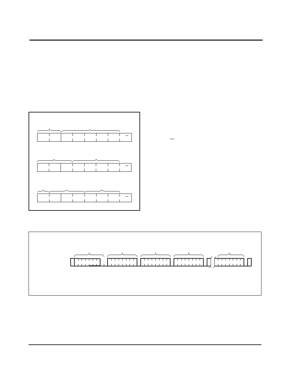
Figure 4. Slave Address
6686 ILL F07.4
S2
A9
A8
R/W
DEVICE
SELECT
S1
A12
HIGH ORDER
SECTOR ADDRESS
A11
A10
X24F064
S2
A9
A8
R/W
DEVICE
SELECT
S1
S0
HIGH ORDER
SECTOR ADDRESS
A11
A10
X24F032
1
A9
A8
R/W
DEVICE
TYPE
IDENTIFIER
S2
S1
HIGH ORDER
SECTOR ADDRESS
S0
A10
X24F016
DEVICE
SELECT
Also included in the slave address is an extension of
the array's address which is concatenated with the
eight bits of address in the sector address field,
providing direct access to the entire SerialFlash
Memory array.
The last bit of the slave address defines the operation
to be performed. When set HIGH a read operation is
selected, when set LOW a program operation is
selected.
Following the start condition, the X24F064/032/016
monitors the SDA bus comparing the slave address
being transmitted with its slave address device type
identifier. Upon a correct comparison of the device
select inputs, the X24F064/032/016 outputs an
acknowledge on the SDA line. Depending on the state
of the R/W bit, the X24F064/032/016 will execute a
read or program operation.
PROGRAMMING OPERATIONS
The X24F064/032/016 offers a 32-byte sector pro-
gramming operation. For a program operation, the
X24F064/032/016 requires a second address field.
This field contains the address of the first byte in the
sector. Upon receipt of the address, comprised of
eight bits, the X24F064/032/016 responds with an ac-
knowledge and awaits the next eight bits of data,
again responding with an acknowledge. The master
then transmits 31 more bytes. After the receipt of
each byte, the X24F064/032/016 will respond with an
acknowledge.
Figure 5. Sector Programming
BUS ACTIVITY:
MASTER
SDA LINE
BUS ACTIVITY:
X24F016/032/064
S
T
A
R
T
SLAVE
ADDRESS
S
S
T
O
P
P
A
C
K
A
C
K
A
C
K
A
C
K
A
C
K
SECTOR ADDRESS
DATA n
DATA n+1
DATA n+31
6686 ILL F10.3