 | –≠–ª–µ–∫—Ç—Ä–æ–Ω–Ω—ã–π –∫–æ–º–ø–æ–Ω–µ–Ω—Ç: X25097SI | –°–∫–∞—á–∞—Ç—å:  PDF PDF  ZIP ZIP |
Document Outline
- Table of Contents
- Product Selection
- Data Sheet Alpha
- Ap Note Alpha
©
Xicor, Inc. 1994, 1995, 1996 Patents Pending
7034-1.1 5/8/97 T1/C0/D0 SH
1
Characteristics subject to change without notice
8K
X25097
1024 x 8 Bit
5MHz Low Power SPI Serial E
2
PROM with IDLock
TM
Memory
FEATURES
∑ 5MHz Clock Rate
∑ IDLockTM Memory
--IDLock First or Last Page, any 1/4 or Lower 1/2
of E
2
PROM Array
∑ Low Power CMOS
--<1
µ
A Standby Current
--<3mA Active Current during Write
--<400
µ
A Active Current during Read
∑ 1.8V to 3.6V, 2.7V-5.5V or 4.5V to 5.5V Operation
∑ Built-in Inadvertent Write Protection
--Power-Up/Power-Down Protection Circuitry
--Write Enable Latch
--Write Protect Pin
∑ SPI Modes (0,0 & 1,1)
∑ 1024 x 8 Bits
--16 Byte Page Mode
∑ Self-Timed Write Cycle
--5ms Write Cycle Time (Typical)
∑ High Reliability
--Endurance: 100,000 Cycles/Byte
--Data Retention: 100 Years
--ESD: 2000V on all pins
∑ 8-Lead TSSOP Package
∑ 8-Lead SOIC Package
∑ 8-Lead PDIP Package
DESCRIPTION
The X25097 is a CMOS 8K-bit serial E
2
PROM, internally
organized as 1024 x 8. The X25097 features a Serial
Peripheral Interface (SPI) and software protocol
allowing operation on a simple four-wire bus. The bus
signals are a clock input (SCK) plus separate data in (SI)
and data out (SO) lines. Access to the device is
controlled through a chip select (CS) input, allowing any
number of devices to share the same bus.
IDLock is a programmble locking mechanism which
allows the user to lock system ID and parametric data in
different portions of the E
2
PROM memory space,
ranging from as little as one page to as much as 1/2 of
the total array. The X25097 also features a WP pin that
can be used for hardwire protection of the part, disabling
all write attempts, as well as a Write Enable Latch that
must be set before a write operation can be initiated.
The X25097 utilizes Xicor's proprietary Direct Write
TM
cell, providing a minimum endurance of 100,000 cycles
per byte and a minimum data retention of 100 years.
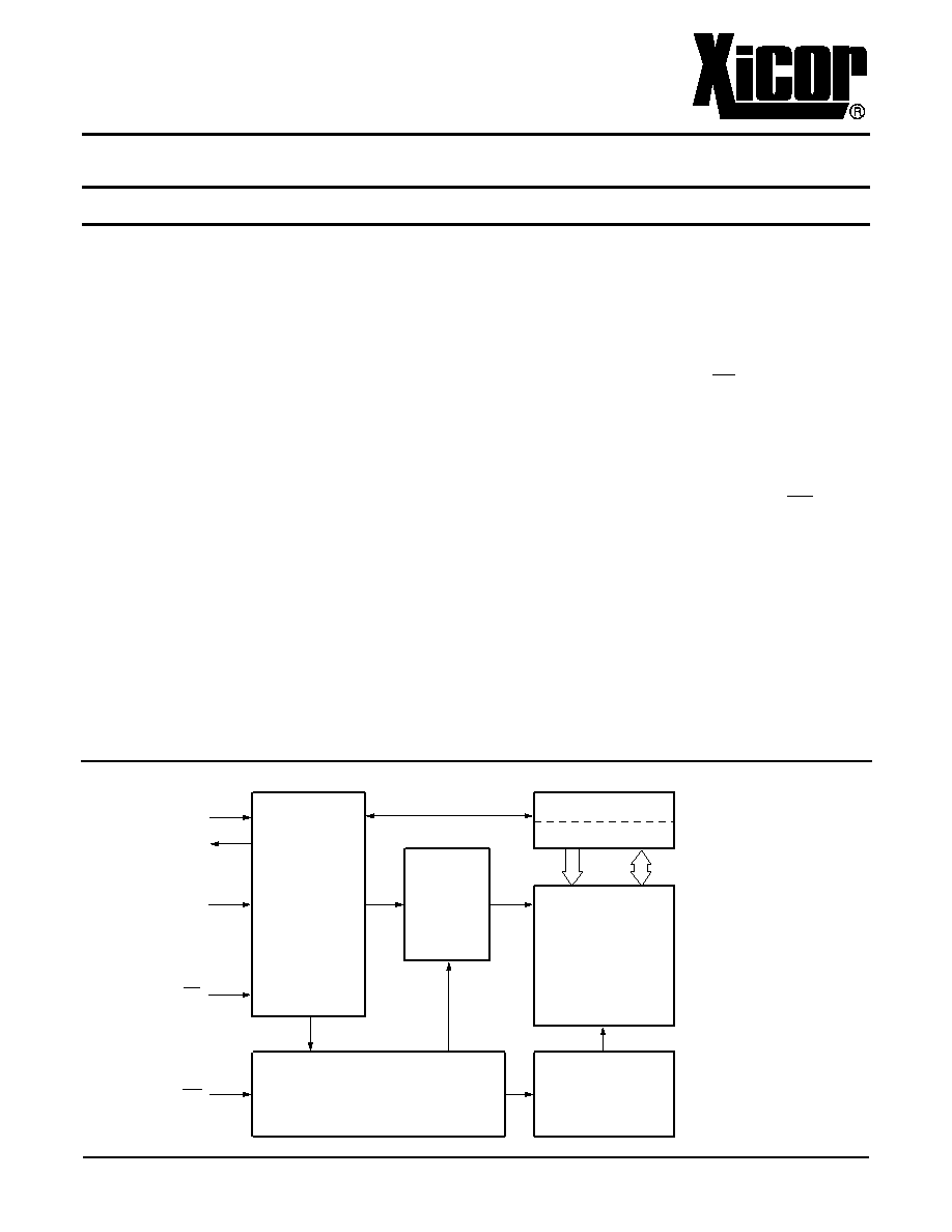
FUNCTIONAL DIAGRAM
COMMAND
DECODE
AND
CONTROL
LOGIC
WRITE CONTROL LOGIC
DATA REGISTER
Y DECODE LOGIC
X
DECODE
LOGIC
HIGH VOLTAGE
CONTROL
8K E
2
PROM
ARRAY
(1024 x 8)
SO
SI
SCK
CS
WP
8
16
64
7038 FRM F01
X25097
2
PIN DESCRIPTIONS
Serial Output (SO)
SO is a push/pull serial data output pin. During a read
cycle, data is shifted out on this pin. Data is clocked out
by the falling edge of the serial clock.
Serial Input (SI)
SI is a serial data input pin. All opcodes, byte addresses,
and data to be written to the memory are input on this
pin. Data is latched by the rising edge of the serial clock.
Serial Clock (SCK)
The Serial Clock controls the serial bus timing for data
input and output. Opcodes, addresses, or data present
on the SI pin are latched on the rising edge of the clock
input, while data on the SO pin change after the falling
edge of the clock input.
Chip Select (CS)
When CS is HIGH, the X25097 is deselected and the SO
output pin is at high impedance and unless an internal
write operation is underway, the X25097 will be in the
standby power mode. CS LOW enables the X25097,
placing it in the active power mode. It should be noted
that after power-up, a HIGH to LOW transition on CS is
required prior to the start of any operation.
Write Protect (WP)
When WP is LOW, nonvolatile writes to the X25097 are
disabled, but the part otherwise functions normally. When
WP is held HIGH, all functions, including nonvolatile
writes operate normally. WP going LOW while CS is still
LOW will interrupt a write to the X25097. If the internal
write cycle has already been initiated, WP going low will
have no affect on this write.
PIN NAMES
7038 FRM T01
PIN CONFIGURATION
PRINCIPLES OF OPERATION
The X25097 is a 1024 x 8 E
2
PROM designed to interface
directly with the synchronous Serial Peripheral Interface
(SPI) of many popular microcontroller families.
The X25097 contains an 8-bit instruction register. It is
accessed via the SI input, with data being clocked in on
the rising edge of SCK. CS must be LOW and the WP
input must be HIGH during the entire operation. Table 1
contains a list of the instructions and their opcodes. All
instructions, addresses and data are transferred MSB first.
Data input is sampled on the first rising edge of SCK
after CS goes LOW. SCK is static, allowing the user to
stop the clock and then start it again to resume opera-
tions where left off.
Write Enable Latch
The X25097 contains a "Write Enable" latch. This latch
must be SET before a write operation is initiated. The
WREN instruction will set the latch and the WRDI instruc-
tion will reset the latch (Figure 4). This latch is automati-
cally reset upon a power-up condition and after the
completion of a byte or page write cycle.
Symbol
Description
CS
Chip Select Input
SO
Serial Output
SI
Serial Input
SCK
Serial Clock Input
WP
Write Protect Input
V
SS
Ground
V
CC
Supply Voltage
NC
No Connect
SCK
SI
VSS
WP
7038 FRM F02.2
NC
VCC
CS
SO
1
2
3
4
8
7
6
5
8 Lead TSSOP
VCC
NC
SCK
SI
7038 FRM F02
CS
SO
WP
VSS
1
2
3
4
8
7
6
5
8 Lead SOIC/PDIP
X25097
X25097
*0.197"
*0.244"
0.122"
0.252"
Not to scale
*SOIC Mesaurement
X25097
3
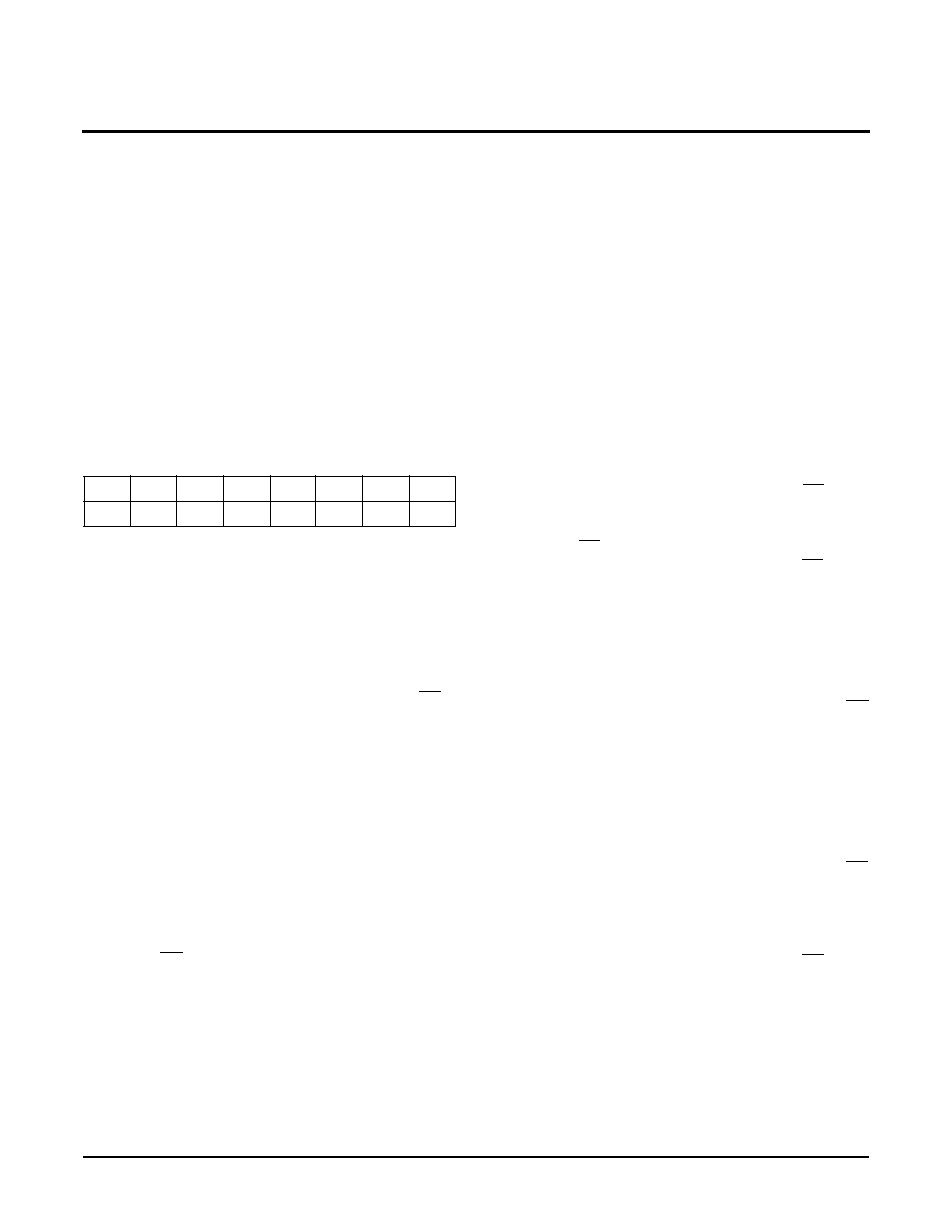
IDLock Memory
Xicor's IDLock Memory provides a flexible mechanism to
store and lock system ID and parametric information.
There are seven distinct IDLock Memory areas within the
array which vary in size from one page to as much as half
of the entire array. These areas and associated address
ranges are IDLocked by writing the appropriate two byte
IDLock instruction to the device as described in Table 1
and Figure 7. Once an IDLock instruction has been com-
pleted, that IDLock setup is held in a nonvolatile Status
Register (Figure 1) until the next IDLock instruction is
issued. The sections of the memory array that are
IDLocked can be read but not written until IDLock Protec-
tion is removed or changed.
Figure 1. Status Register/IDLock Byte
Clock and Data Timing
Data input on the SI line is latched on the rising edge of
SCK. Data is output on the SO line by the falling edge of
SCK.
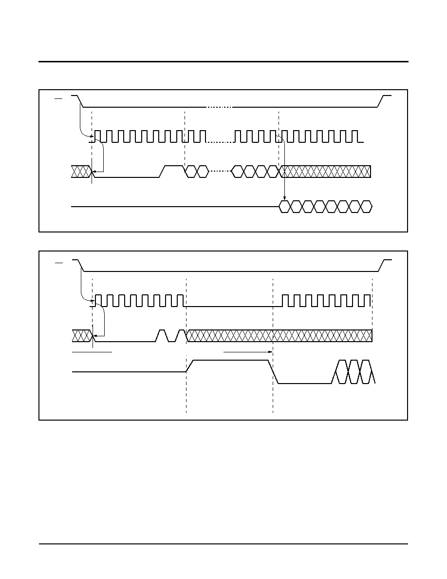
Read Sequence
When reading from the E
2
PROM memory array, CS is
first pulled LOW to select the device. The 8-bit READ
instruction is transmitted to the X25097, followed by the
16-bit address, of which the last 10 bits are used (bits
[15:10] specified to be zeroes). After the READ opcode
and address are sent, the data stored in the memory at
the selected address is shifted out on the SO line. The
data stored in memory at the next address can be read
sequentially by continuing to provide clock pulses. The
address is automatically incremented to the next higher
address after each byte of data is shifted out. When the
highest address is reached (03FFh), the address counter
rolls over to address 0000h, allowing the read cycle to be
continued indefinitely. The read operation is terminated
by taking CS HIGH. Refer to the Read Operation
Sequence illustrated in Figure 2.
Read Status Operation
If there is not a nonvolatile write in progress, the Read
Status instruction returns the ID Lock byte from the Sta-
tus Register which contains the ID Lock bits IDL2-IDL0
(Figure 1). The ID Lock bits define the ID Lock condition
(Figure 1/Table1). The other bits are reserved and will
return '0' when read. See Figure 3.
If a nonvolatile write is in progress, the Read Status
Instruction returns a HIGH on SO. When the nonvolatile
write cycle is completed, the status register data is read
out.
Clocking SCK is valid during a nonvolatile write in
progress, but is not necessary. If the SCK line is clocked,
the pointer to the status register is also clocked, even
though the SO pin shows the status of the nonvolatile
write operation (See Figure 3).
Write Sequence
Prior to any attempt to write data into the X25097, the
"Write Enable" latch must first be set by issuing the
WREN instruction (See Table 1 and Figure 4). CS is first
taken LOW. Then the WREN instruction is clocked into
the X25097. After all eight bits of the instruction are
transmitted, CS must then be taken HIGH. If the user
continues the write operation without taking CS HIGH
after issuing the WREN instruction, the write operation
will be ignored.
To write data to the E
2
PROM memory array, the user then
issues the WRITE instruction, followed by the 16 bit
address and the data to be written. Only the last 10 bits of
the address are used and bits [15:10] are specified to be
zeroes. This is minimally a thirty-two clock operation. CS
must go LOW and remain LOW for the duration of the
operation. The host may continue to write up to 16 bytes
of data to the X25097. The only restriction is the 16 bytes
must reside on the same page. If the address counter
reaches the end of the page and the clock continues, the
counter will "roll over" to the first address of the page and
overwrite any data that may have been previously written.
For a byte or page write operation to be completed, CS
can only be brought HIGH after bit 0 of the last data byte
to be written is clocked in. If it is brought HIGH at any
other time, the write operation will not be completed.
Refer to Figures 5 and 6 for detailed illustration of the
write sequences and time frames in which CS going
HIGH are valid.
7
6
5
4
3
2
1
0
0
0
0
0
0
IDL2 IDL1 IDL0
Note: Bits [7:3] specified to be "0's"
7038 FRM T02.1
X25097
4
IDLock Operation
Prior to any attempt to perform an IDLock Operation, the
WREN instruction must first be issued. This instruction
sets the "Write Enable" latch and allows the part to
respond to an IDLock sequence (Figure 7). The IDLock
instruction follows and consists of one command byte fol-
lowed by one IDLock byte (See Figure 1). This byte con-
tains the IDLock bits IDL2-IDL0. The rest of the bits [7:3]
are unused and must be written as zeroes. Bringing CS
HIGH after the two byte IDLock instruction initiates a
nonvolatile write to the Status Register. Writing more
than one byte to the Status Register will overwrite the
previously written IDLock byte. See Table 1.
Operational Notes
The X25097 powers up in the following state:
∑ The device is in the low power, standby state.
∑ A HIGH to LOW transition on CS is required to enter
an active state and receive an instruction.
∑ SO pin is at high impedance.
∑ The "Write Enable" latch is reset.
Data Protection
The following circuitry has been included to prevent inad-
vertant writes:
∑ The "Write Enable" latch is reset upon power-up.
∑ A WREN instruction must be issued to set the "Write
Enable" latch.
∑ CS must come HIGH at the proper clock count in order
to start a write cycle.
Table 1. Instruction Set and Block Lock Protection Byte Definition
7038 FRM T03
*Instructions are shown with MSB in leftmost position. Instructions are transferred MSB first.
Instruction Format*
Instruction Name and Operation
0000 0110
WREN: Set the Write Enable Latch (Write Enable Operation)
0000 0100
WRDI: Reset the Write Enable Latch (Write Disable Operation)
0000 0001
IDLock Instruction--followed by:
IDLock Byte: (See Figure 1)
0000 0000 --->NO IDLock: 00h-00h - - - - - - - - - - - >None of the Array
0000 0001 --->IDLock Q1: 0000h-00FFh - - - - - - - >Lower Quadrant (Q1)
0000 0010 --->IDLock Q2: 0100h-01FFh - - - - - - - >Q2
0000 0011 --->IDLock Q3: 0200h-02FFh - - - - - - - >Q3
0000 0100 --->IDLock Q4: 0300h-03FFh - - - - - - - >Upper Quadrant (Q4)
0000 0101 --->IDLock H1: 0000h-01FFh - - - - - - - >Lower Half of the Array (H1)
0000 0110 --->IDLock P0: 0000h-000Fh - - - - - - - >Lower Page (P0)
0000 0111 --->IDLock Pn: 03F0h-03FFh - - - - - - - >Upper Page (Pn)
0000 0101
READ STATUS: Reads IDLock & write in progress status on SO Pin
0000 0010
WRITE: Write operation followed by address and data
0000 0011
READ: Read operation followed by address
X25097
5
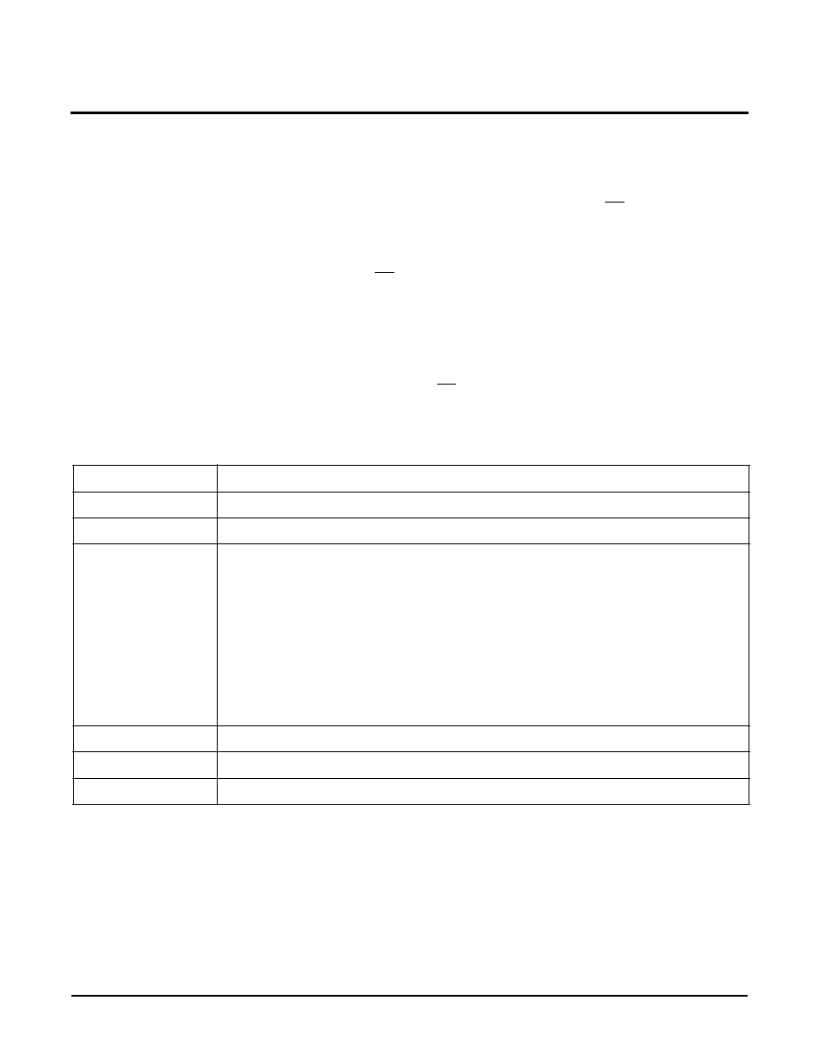
Figure 2. Read Operation Sequence
Figure 3. Read Status Operation Sequence
0
1
2
3
4
5
6
7
8
9
CS
SCK
SI
SO
HIGH IMPEDANCE
READ INSTRUCTION
(1 BYTE)
BYTE ADDRESS (2 BYTE)
DATA OUT
15 14
3
2
1
0
20 21 22 23 24 25 26 27 28 29 30
7038 FRM F03.1
7
6
5
4
3
2
1
0
0
1
2
3
4
5
6
7
CS
SCK
SI
SO
NONVOLATILE WRITE IN PROGRESS
READ STATUS
INSTRUCTION
7038 FRM F04.2
SO HIGH DURING
NONVOLATILE
WRITE CYCLE
SO = STATUS REG BIT
WHEN NO NONVOLATILE
WRITE CYCLE
...
...
...
I
D
L
2
I
D
L
1
I
D
L
0