5MHz SPI Serial E
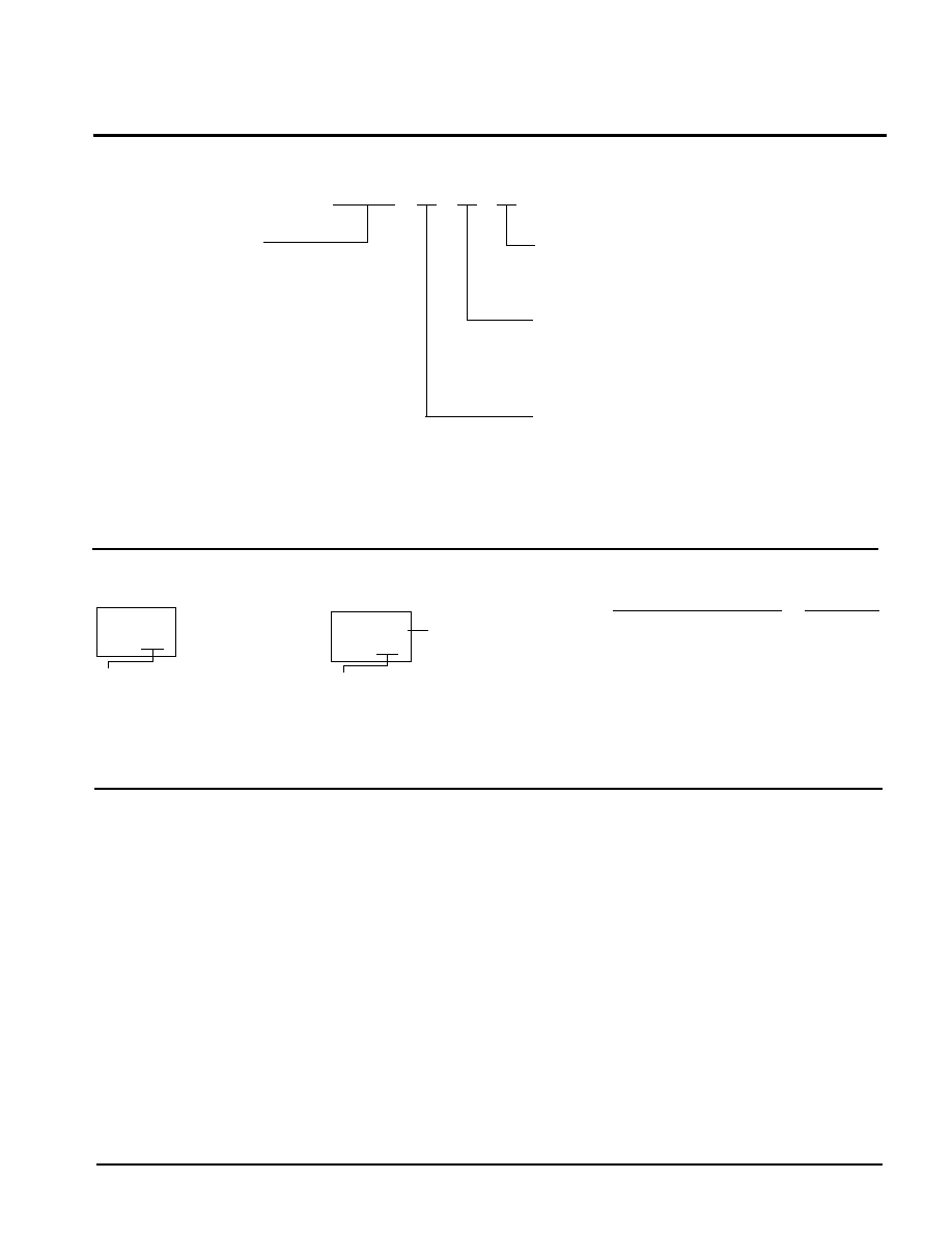
2
PROM with Block Lock
TM
Protection
128K
16K x 8 Bit
”
Xicor, Inc. 1998 Patents Pending
1
Characteristics subject to change without notice
7056≠1.5 8/13/98 T2/C0/D1 EW
X25138
FEATURES
∑
5MHz Clock Rate
∑
Low Power CMOS
<1
m
A Standby Current
<5mA Active Current
∑
2.5V To 5.5V Power Supply
∑
SPI Modes (0,0 & 1,1)
∑
16K X 8 Bits
32 Byte Page Mode
∑
Block LockTM Protection
Protect 1/4, 1/2 or all of E
2
PROM Array
∑
Programmable Hardware Write Protection
In-Circuit Programmable ROM Mode
∑
Built-in Inadvertent Write Protection
Power-Up/Down protection circuitry
Write Enable Latch
Write Protect Pin
∑
Self-Timed Write Cycle
5ms Write Cycle Time (Typical)
∑
High Reliability
Endurance: 100,000 cycles
Data Retention: 100 Years
ESD protection: 2000V on all pins
∑
Packages
8-Lead XBGA
8, 14-Lead SOIC
8-Lead PDIP
8-Lead TSSOP
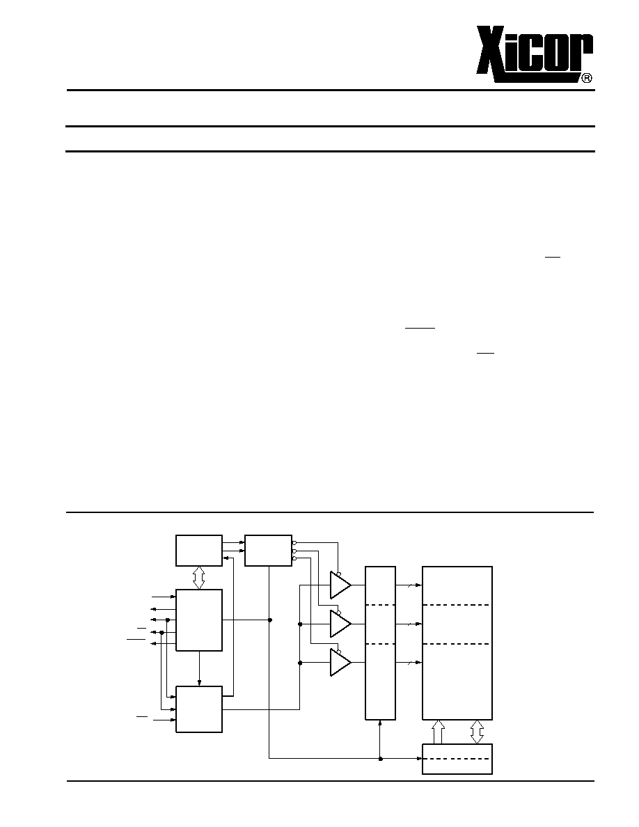
DESCRIPTION
The X25138 is a CMOS 128K-bit serial E
2
PROM,
internally organized as 16K x 8. The X25138 features
a Serial Peripheral Interface (SPI) and software
protocol allowing operation on a simple three-wire bus.
The bus signals are a clock input (SCK) plus separate
data in (SI) and data out (SO) lines. Access to the
device is controlled through a chip select (CS) input,
allowing any number of devices to share the same
bus.
The X25138 also features two additional inputs that
provide the end user with added flexibility. By
asserting the HOLD input, the X25138 will ignore tran-
sitions on its inputs, thus allowing the host to service
higher priority interrupts. The WP input can be used as
a hardwire input to the X25138 disabling all write
attempts to the status register, thus providing a mech-
anism for limiting end user capability of altering 0, 1/4,
1/2 or all of the memory.
The X25138 utilizes Xicor's proprietary Direct Write
TM
cell, providing a minimum endurance of 100,000
cycles and a minimum data retention of 100 years.
COMMAND
DECODE
AND
CONTROL
LOGIC
WRITE
CONTROL
AND
TIMING
LOGIC
WRITE
PROTECT
LOGIC
X DECODE
LOGIC
16K BYTE
ARRAY
128 X 256
Y DECODE
DATA REGISTER
SO
SI
SCK
CS
HOLD
WP
128
256
8
32
STATUS
REGISTER
128
256 X 256
128 X 256
7037 FRM F01
Direct Write
‘
and Block Lock
‘
Protection is a trademark of Xicor, Inc.
FUNCTIONAL DIAGRAM
X25138
2
PIN DESCRIPTIONS
Serial Output (SO)
SO is a push/pull serial data output pin. During a read
cycle, data is shifted out on this pin. Data is clocked
out by the falling edge of the serial clock.
Serial Input (SI)
SI is the serial data input pin. All opcodes, byte
addresses, and data to be written to the memory are
input on this pin. Data is latched by the rising edge of
the serial clock.
Serial Clock (SCK)
The Serial Clock controls the serial bus timing for data
input and output. Opcodes, addresses, or data present
on the SI pin are latched on the rising edge of the
clock input, while data on the SO pin change after the
falling edge of the clock input.
Chip Select (CS)
When CS is HIGH, the X25138 is deselected and the
SO output pin is at high impedance and unless an
internal write operation is underway, the X25138 will be
in the standby power mode. CS LOW enables the
X25138, placing it in the active power mode. It should
be noted that after power-up, a HIGH to LOW transition
on CS is required prior to the start of any operation.
Write Protect (WP)
When WP is LOW and the nonvolatile bit WPEN is "1",
nonvolatile writes to the X25138 status register are
disabled, but the part otherwise functions normally.
When WP is held HIGH, all functions, including
nonvolatile writes operate normally. WP going LOW
while CS is still LOW will interrupt a write to the
X25138 status register. If the internal write cycle has
already been initiated, WP going LOW will have no
affect on a write.
The WP pin function is blocked when the WPEN bit in
the status register is "0". This allows the user to install
the X25138 in a system with WP pin grounded and still
be able to write to the status register. The WP pin func-
tions will be enabled when the WPEN bit is set "1".
Hold (HOLD)
HOLD is used in conjunction with the CS pin to pause
the device. Once the part is selected and a serial
sequence is underway, HOLD may be used to pause
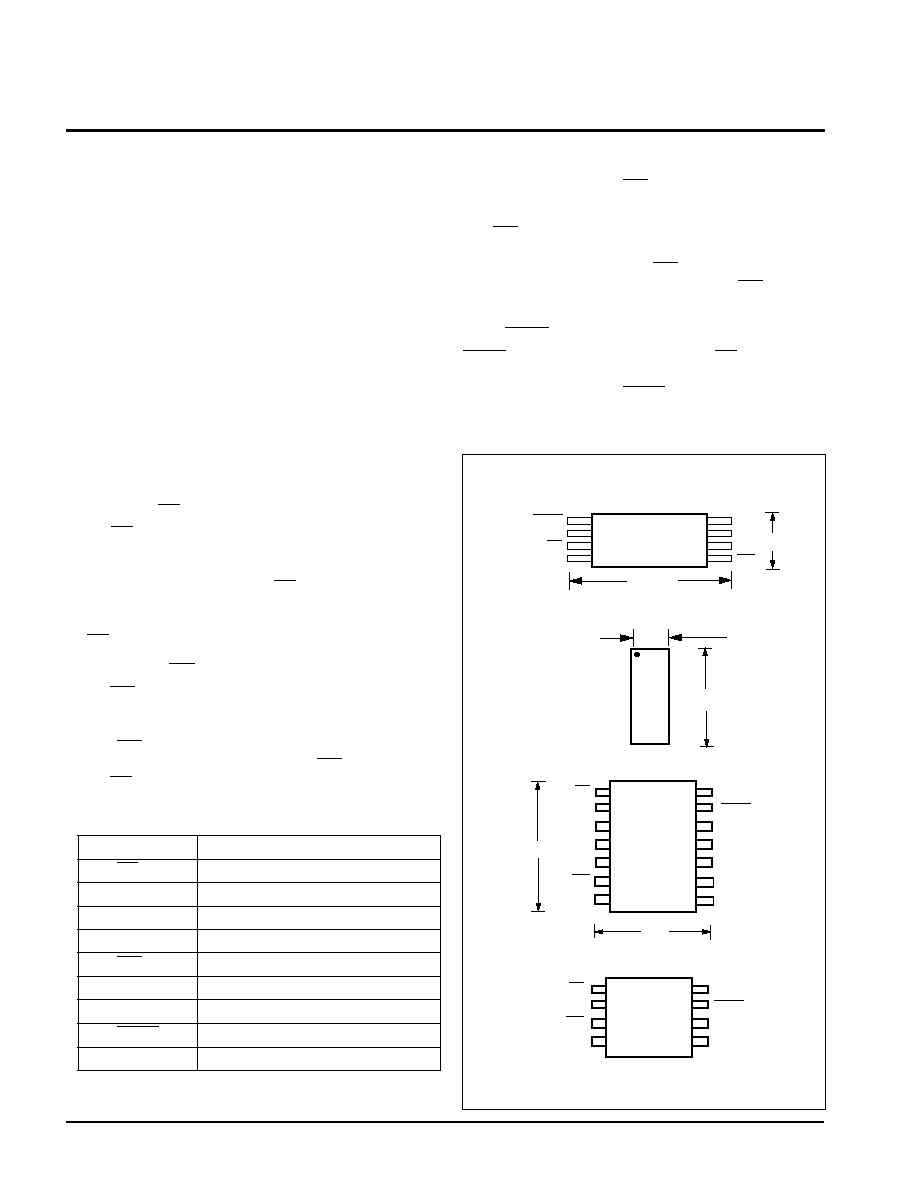
14 Lead SOIC
NC
1
2
3
4
7
6
5
X25138
VSS
NC
NC
NC
NC
.228"
.336"
8
9
10
11
12
14
13
NC
8 Lead PDIP/SOIC
VCC
HOLD
SCK
CS
1
2
3
4
6
7
8
X25138
VSS
SI
5
SO
WP
CS
SO
WP
VCC
HOLD
SCK
SI
8-Lead XBGA: Top View
S0
SI
WP
SCK
V
CC
V
SS
CS
HOLD
8
7
6
5
1
2
3
4
.238"
SCK
1
2
3
4
8
7
6
5
8-LEAD TSSOP
X25138
.252 in.
SI
Vss
CS
HOLD
WP
.078"
SO
Vcc
3091 FM 03
.114"
PIN NAMES
7037 FRM T01
Symbol
Description
CS
Chip Select Input
SO
Serial Output
SI
Serial Input
SCK
Serial Clock Input
WP
Write Protect Input
V
SS
Ground
V
CC
Supply Voltage
HOLD
Hold Input
NC
No Connect
PIN CONFIGURATION
X25138
3
the serial communication with the controller without
resetting the serial sequence. To pause, HOLD must
be brought LOW while SCK is LOW. To resume
communication,
HOLD is brought HIGH, again while
SCK is LOW. If the pause feature is not used, HOLD
should be held HIGH at all times.
PRINCIPLES OF OPERATION
The X25138 is a 16K x 8 E
2
PROM designed to inter-
face directly with the synchronous serial peripheral
interface (SPI) of many popular microcontroller fami-
lies.
The X25138 contains an 8-bit instruction register. It is
accessed via the SI input, with data being clocked in on
the rising SCK. CS must be LOW and the HOLD and
WP inputs must be HIGH during the entire operation.
Table 1 contains a list of the instructions and their
opcodes. All instructions, addresses and data are
transferred MSB first.
Data input is sampled on the first rising edge of SCK
after CS goes LOW. SCK is static, allowing the user to
stop the clock and then resume operations. If the clock
line is shared with other peripheral devices on the SPI
bus, the user can assert the
HOLD input to place the
X25138 into a "PAUSE" condition. After releasing
HOLD, the X25138 will resume operation from the
point when HOLD was first asserted.
Write Enable Latch
The X25138 contains a "write enable" latch. This latch
must be SET before a write operation will be
completed internally. The WREN instruction will set the
latch and the WRDI instruction will reset the latch. This
latch is automatically reset upon a power-up condition
and after the completion of a byte, page, or status
register write cycle.
Status Register
The RDSR instruction provides access to the status
register. The status register may be read at any time,
even during a write cycle. The status register is
formatted as follows:
7037 FRM T02
WPEN, BL0 and BL1 are set by the WRSR instruction.
WEL and WIP are read-only and automatically set by
other operations.
The Write-In-Process (WIP) bit indicates whether the
X25138 is busy with a write operation. When set to a
"1", a write is in progress, when set to a "0", no write is
in progress. During a write, all other bits are set to "1".
The Write Enable Latch (WEL) bit indicates the status
of the "write enable" latch. When set to a "1", the latch
is set, when set to a "0", the latch is reset.
The Block Lock (BL0 and BL1) bits are nonvolatile and
allow the user to select one of four levels of protection.
The X25138 is divided into four 32K-bit segments.
One, two, or all four of the segments may be protected.
That is, the user may read the segments but will be
unable to alter (write) data within the selected
segments. The partitioning is controlled as illustrated
below.
7037 FRM T03
7
6
5
4
3
2
1
0
WPEN
X
X
X
BL1
BL0
WEL
WIP
Status Register Bits
Array Addresses
Protected
BL1
BL0
0
0
None
0
1
$3000≠$3FFF
1
0
$2000≠$3FFF
1
1
$0000≠$3FFF
Table 1. Instruction Set
7037 FRM T04
*Instructions are shown MSB in leftmost position. Instructions are transferred MSB first.
Instruction Name
Instruction Format*
Operation
WREN
0000 0110
Set the Write Enable Latch (Enable Write Operations)
WRDI
0000 0100
Reset the Write Enable Latch (Disable Write Operations)
RDSR
0000 0101
Read Status Register
WRSR
0000 0001
Write Status Register
READ
0000 0011
Read Data from Memory Array beginning at selected address
WRITE
0000 0010
Write Data to Memory Array beginning at Selected Address (1 to 32
Bytes)
X25138
4
The Write-Protect-Enable (WPEN) bit is available for
the X25138 as a nonvolatile enable bit for the WP pin.
7037 FRM T05
Programmable Hardware Write Protection
The Write Protect (WP) pin and the nonvolatile Write
Protect Enable (WPEN) bit in the Status Register
control the Programmable Hardware Write Protect
feature. Hardware Write Protection is enabled when
WP pin is LOW, and the WPEN bit is "1". Hardware
Write Protection is disabled when either the WP pin is
HIGH or the WPEN bit is "0". When the chip is hard-
ware write protected, nonvolatile writes are disabled to
the Status Register, including the Block Lock bits and
the WPEN bit itself, as well as the block-protected
sections in the memory array. Only the sections of the
memory array that are not block-protected can be
written.
In Circuit Programmable ROM Mode
Note that since the WPEN bit is write protected, it
cannot be changed back to a LOW state; so write
protection is enabled as long as the WP pin is held
LOW. Thus an In Circuit Programmable ROM function
can be emplemented by hardwiring the WP pin to Vss,
writing to and Block Locking the desired portion of the
array to be ROM, and then programming the WPEN bit
HIGH. The table above defines the program protect
status for each combination of WPEN and
WP
.
Clock and Data Timing
Data input on the SI line is latched on the rising edge
of SCK. Data is output on the SO line by the falling
edge of SCK.
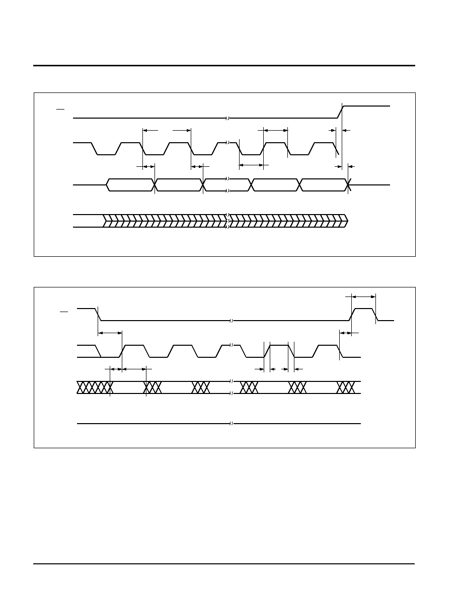
Read Sequence
When reading from the E
2
PROM memory array, CS is
first pulled LOW to select the device. The 8-bit READ
instruction is transmitted to the X25138, followed by
the 16-bit address of which the last 14 are used. After
the READ opcode and address are sent, the data
stored in the memory at the selected address is
shifted out on the SO line. The data stored in memory
WPEN
WP
WEL
Protected
Blocks
Unprotected
Blocks
Status
Register
0
X
0
Protected
Protected
Protected
0
X
1
Protected
Writable
Writable
1
LOW
0
Protected
Protected
Protected
1
LOW
1
Protected
Writable
Protected
X
HIGH
0
Protected
Protected
Protected
X
HIGH
1
Protected
Writable
Writable
at the next address can be read sequentially by
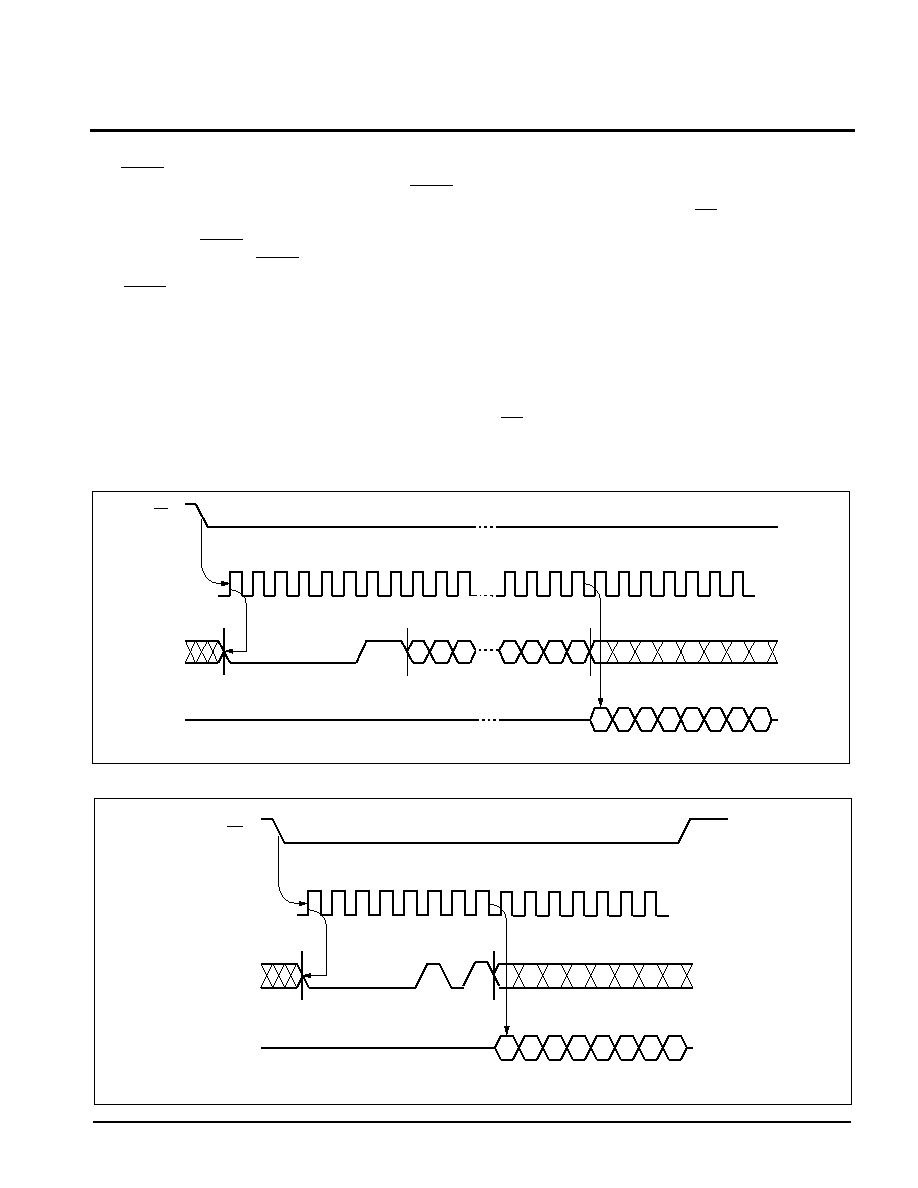
continuing to provide clock pulses. The address is
automatically incremented to the next higher address
after each byte of data is shifted out. When the highest
address is reached ($3FFF) the address counter rolls
over to address $0000 allowing the read cycle to be
continued indefinitely. The read operation is termi-
nated by taking CS HIGH. Refer to the read E
2
PROM
array operation sequence illustrated in Figure 1.
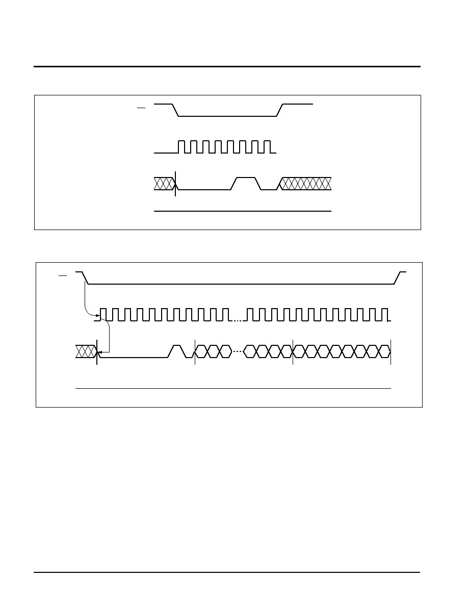
To read the status register the CS line is first pulled
LOW to select the device followed by the 8-bit RDSR
instruction. After the RDSR opcode is sent, the contents
of the status register are shifted out on the SO line.
Figure 2 illustrates the read status register sequence.
Write Sequence
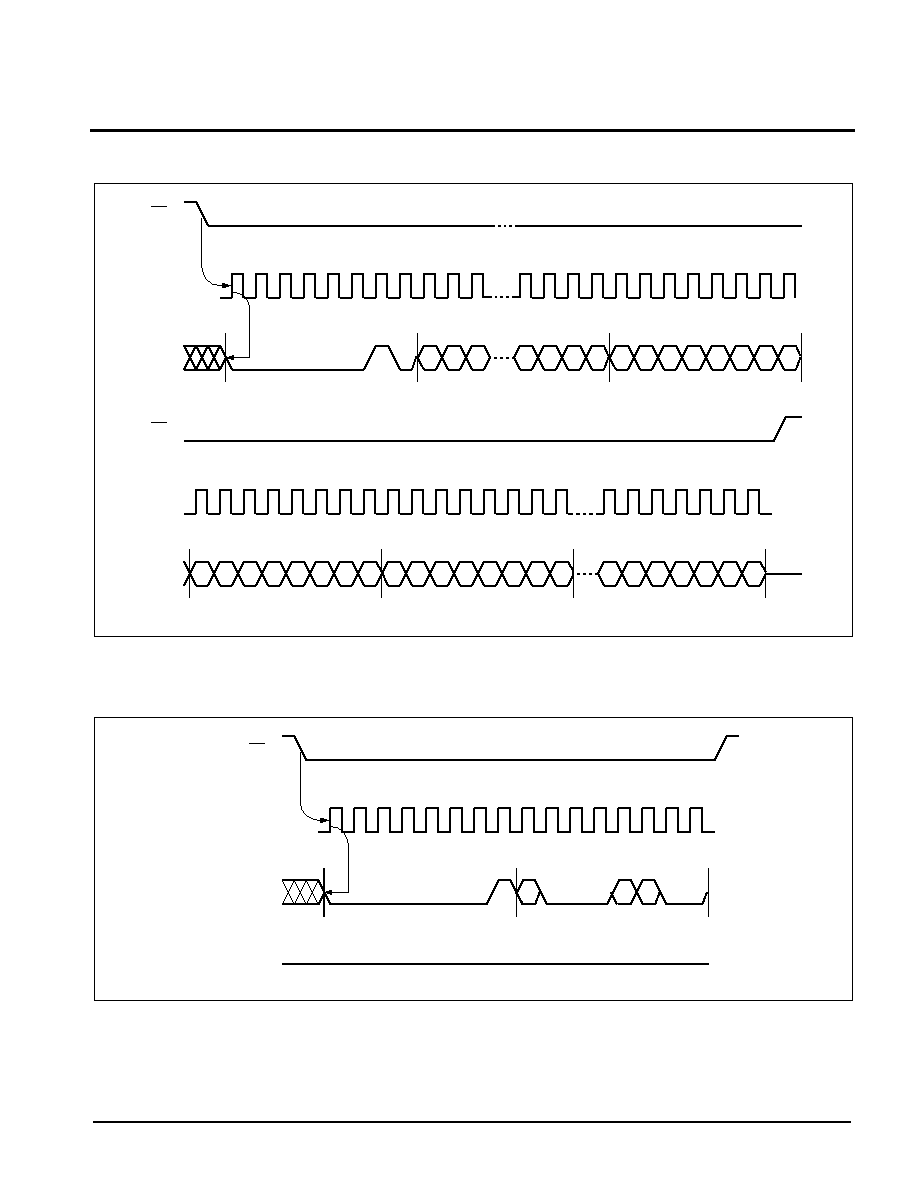
Prior to any attempt to write data into the X25138, the
"write enable" latch must first be set by issuing the
WREN instruction (See Figure 3). CS is first taken
LOW, then the WREN instruction is clocked into the
X25138. After all eight bits of the instruction are trans-
mitted, CS must then be taken HIGH. If the user
continues the write operation without taking CS HIGH
after issuing the WREN instruction, the write operation
will be ignored.
To write data to the E
2
PROM memory array, the user
issues the WRITE instruction, followed by the address
and then the data to be written. This is minimally a
thirty-two clock operation. CS must go LOW and remain
LOW for the duration of the operation. The host may
continue to write up to 32 bytes of data to the X25138.
The only restriction is the 32 bytes must reside on the
same page. If the address counter reaches the end of
the page and the clock continues, the counter will "roll
over" to the first address of the page and overwrite any
data that may have been written.
For the write operation (byte or page write) to be
completed, CS can only be brought HIGH after bit 0 of
data byte N is clocked in. If it is brought HIGH at any
other time the write operation will not be completed.
Refer to Figures 4 and 5 below for a detailed illustra-
tion of the write sequences and time frames in which
CS going HIGH are valid.
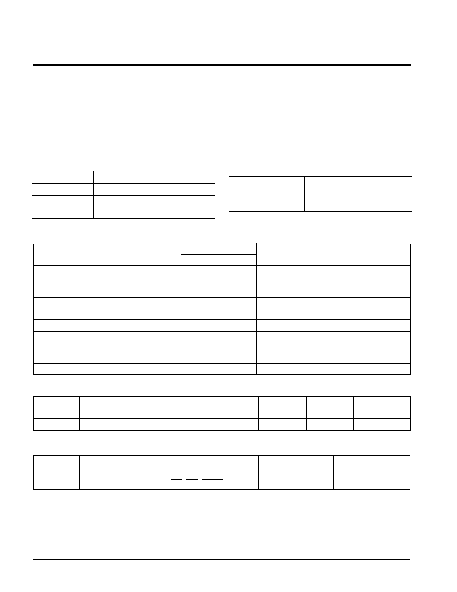
To write to the status register, the WRSR instruction is
followed by the data to be written. Data bits 0, 1, 4, 5
and 6 must be "0". Figure 6 illustrates this sequence.
While the write is in progress following a status
register or E
2
PROM write sequence, the status
register may be read to check the WIP bit. During this
time the WIP bit will be HIGH.
X25138
5
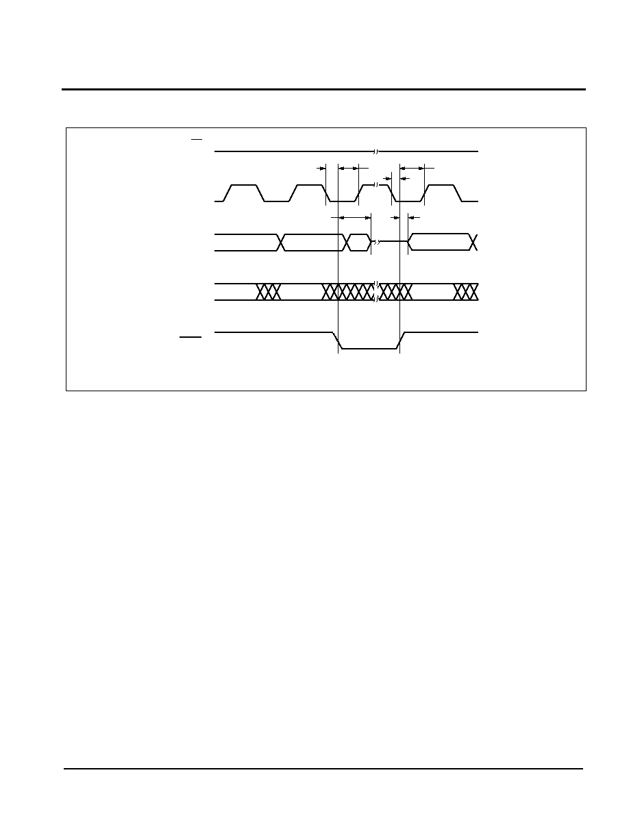
Hold Operation
The HOLD input should be HIGH (at V
IH
) under normal
operation. If a data transfer is to be interrupted HOLD
can be pulled LOW to suspend the transfer until it can
be resumed. The only restriction is the SCK input must
be LOW when HOLD is first pulled LOW and SCK
must also be LOW when HOLD is released.
The HOLD input may be tied HIGH either directly to
V
CC
or tied to V
CC
through a resistor.
Operational Notes
The X25138 powers-up in the following state:
∑ The device is in the low power standby state.
∑ A HIGH to LOW transition on CS is required to enter
an active state and receive an instruction.
∑ SO pin is high impedance.
∑ The "write enable" latch is reset.
Data Protection
The following circuitry has been included to prevent in-
advertent writes:
∑ The "write enable" latch is reset upon power-up.
∑ A WREN instruction must be issued to set the "write
enable" latch.
∑ CS must come HIGH at the proper clock count in or-
der to start a write cycle.
Figure 1. Read E
2
PROM Array Operation Sequence
0
1
2
3
4
5
6
7
8
9
10
20 21 22 23 24
25 26 27 28 29
30
7
6
5
4
3
2
1
0
DATA OUT
CS
SCK
SI
SO
MSB
HIGH IMPEDANCE
INSTRUCTION
16 BIT ADDRESS
15 14 13
3
2
1
0
7037 FRM F03
Figure 2. Read Status Register Operation Sequence
0
1
2
3
4
5
6
7
8
9
10 11
12 13 14
7
6
5
4
3
2
1
0
DATA OUT
CS
SCK
SI
SO
MSB
HIGH IMPEDANCE
INSTRUCTION
7037 FRM F04
X25138
6
Figure 3. Write Enable Latch Sequence
Figure 4. Byte Write Operation Sequence
0
1
2
3
4
5
6
7
7037 FRM F05
CS
SI
SCK
HIGH IMPEDANCE
SO
0
1
2
3
4
5
6
7
8
9
10
CS
SCK
SI
SO
HIGH IMPEDANCE
INSTRUCTION
16 BIT ADDRESS
DATA BYTE
7
6
5
4
3
2
1
0
15 14 13
3
2
1
0
20 21 22 23 24 25 26 27 28 29 30 31
7037 FRM F06
X25138
7
Figure 6. Write Status Register Operation Sequence
Figure 5. Page Write Operation Sequence
32 33 34 35 36 37 38 39
SCK
SI
CS
0
1
2
3
4
5
6
7
8
9
10
SCK
SI
INSTRUCTION
16 BIT ADDRESS
DATA BYTE 1
7
6
5
4
3
2
1
0
CS
40 41 42 43 44 45 46 47
DATA BYTE 2
7
6
5
4
3
2
1
0
DATA BYTE 3
7
6
5
4
3
2
1
0
DATA BYTE N
15 14 13
3
2
1
0
20 21 22 23 24 25 26 27 28 29 30 31
6
5
4
3
2
1
0
7037 FRM F07
0
1
2
3
4
5
6
7
8
9
CS
SCK
SI
SO
HIGH IMPEDANCE
INSTRUCTION
DATA BYTE
7
6
5
4
3
2
1
0
10
11 12 13 14 15
7037 FRM F08
X25138
8
ABSOLUTE MAXIMUM RATINGS*
Temperature under Bias....................≠65
∞
C to +135
∞
C
Storage Temperature ........................≠65
∞
C to +150
∞
C
Voltage on any Pin with Respect
to V
SS
.........................................................≠1V to +7V
D.C. Output Current ............................................. 5mA
(Soldering, 10 seconds) ..............................300
∞
C
D.C. OPERATING CHARACTERISTICS
(Over the recommended operating conditions unless otherwise specified.)
7037 FRM T08
POWER-UP TIMING
7037 FRM T09
CAPACITANCE
T
A
= +25
∞
C, f = 1MHz, V
CC
= 5V
7037 FRM T10
Notes:
(1) V
IL
min. and V
IH
max. are for reference only and are not tested.
(2) This parameter is periodically sampled and not 100% tested.
(3) t
PUR
and t
PUW
are the delays required from the time V
CC
is stable until the specified operation can be initiated. These
parameters are periodically sampled and not 100% tested.
Symbol
Parameter
Limits
Units
Test Conditions
Min.
Max.
I
CC
V
CC
Supply Current (Active)
5
mA
SCK = V
CC
x 0.1/V
CC
x 0.9 @ 5MHz,
I
SB
V
CC
Supply Current (Standby)
1
m
A
CS
= V
CC
, V
IN
=
V
SS
or V
CC
≠ 0.3V
I
LI
Input Leakage Current
10
m
A
V
IN
=
V
SS
to V
CC
I
LO
Output Leakage Current
10
m
A
V
OUT
=
V
SS
to V
CC
V
IL
(1)
Input LOW Voltage
≠1
V
CC
x 0.3
V
V
IH
(1)
Input HIGH Voltage
V
CC
x 0.7
V
CC
+ 0.5
V
V
OL1
Output LOW Voltage
0.4
V
I
OL
= 3mA, V
CC
= 5V
V
OH1
Output HIGH Voltage
V
CC
≠0.8
V
I
OH
= ≠1.6mA, V
CC
= 5V
V
OL2
Output LOW Voltage
0.4
V
I
OL
= 1.5mA, V
CC
= 3V
V
OH2
Output HIGH Voltage
V
CC
≠0.3
V
I
OH
= ≠0.4mA, V
CC
= 3V
Symbol
Parameter
Min.
Max.
Units
T
PUR
(3)
Power-up to Read Operation
1
ms
T
PUW
(3)
Power-up to Write Operation
1
ms
Symbol
Parameter
Max.
Units
Test Conditions
C
I/O
(3)
Output Capacitance (SO)
8
pF
V
I/O
= 0V
C
IN
(3)
Input Capacitance (SCK, SI,
CS
,
WP
,
HOLD
)
6
pF
V
IN
= 0V
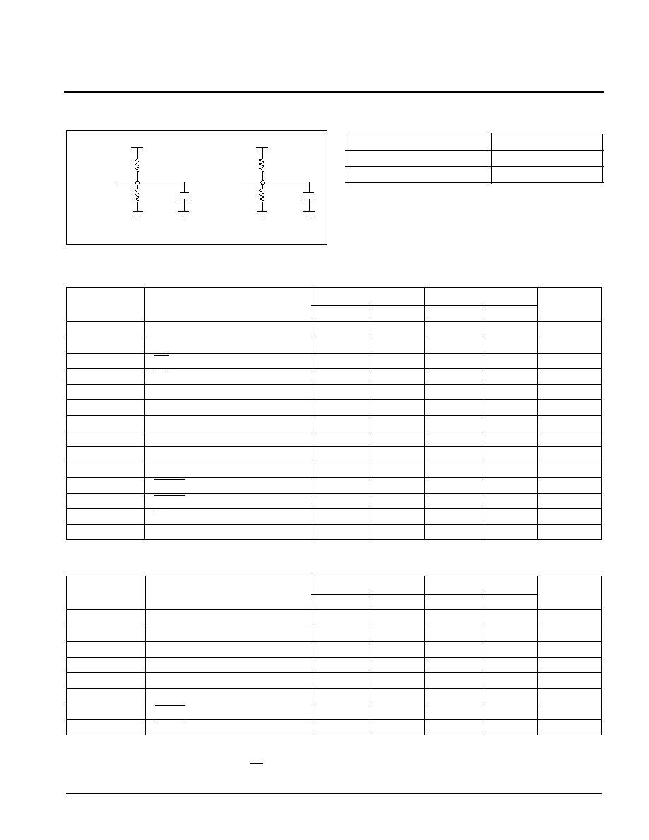
RECOMMENDED OPERATING CONDITIONS
7037 FRM T06
Temperature
Min.
Max.
Commercial
0
∞
C
+70
∞
C
Industrial
≠40
∞
C
+85
∞
C
Military
≠55
∞
C
+125
∞
C
7037 FRM T07
Supply Voltage
Limits
X25138
5V
±
10%
X25138-2.5
2.5V to 5.5V
*COMMENT
Stresses above those listed under "Absolute Maximum
Ratings" may cause permanent damage to the device.
This is a stress rating only and the functional operation
of the device at these or any other conditions above
those indicated in the operational sections of this
specification is not implied. Exposure to absolute
maximum rating conditions for extended periods may
affect device reliability.
X25138
9
A.C. OPERATING CHARACTERISTICS
Data Input Timing
7037 FRM T12
Data Output Timing
7037 FRM T13
Notes: (4) This parameter is periodically sampled and not 100% tested.
(5) t
WC
is the time from the rising edge of CS after a valid write sequence has been sent to the end of the self-timed internal nonvolatile
write cycle
Symbol Parameter
V
CC
= 2.5V-5.5V
V
CC
= 4.5V-5.5V
Units
Min.
Max.
Min.
Max.
f
SCK
Clock Frequency
0
3.3
0
5
MHz
t
CYC
Cycle Time
300
200
ns
t
LEAD
CS Lead Time
150
100
ns
t
LAG
CS Lag Time
150
100
ns
t
WH
Clock HIGH Time
130
80
ns
t
WL
Clock LOW Time
130
80
ns
t
SU
Data Setup Time
30
20
ns
t
H
Data Hold Time
30
20
ns
t
RI
(4)
Data In Rise Time
2
2
m
s
t
FI
(4)
Data In Fall Time
2
2
m
s
t
HD
HOLD
Setup Time
60
40
ns
t
CD
HOLD
Hold Time
60
40
ns
t
CS
CS
Deselect Time
100
100
ns
t
WC
(5)
Write Cycle Time
10
10
ms
Symbol Parameter
V
CC
= 2.5V-5.5V
V
CC
= 4.5V-5.5V
Units
Min.
Max.
Min.
Max.
f
SCK
Clock Frequency
0
3.3
0
5
MHz
t
DIS
Output Disable Time
150
100
ns
t
V
Output Valid from Clock LOW
130
80
ns
t
HO
Output Hold Time
0
0
ns
t
RO
(4)
Output Rise Time
50
50
ns
t
FO
(4)
Output Fall Time
50
50
ns
t
LZ
(4)
HOLD
HIGH to Output in Low Z
50
50
ns
t
HZ
(4)
HOLD
LOW to Output in High Z
50
50
ns
A.C. CONDITIONS OF TEST
7037 FRM T11
Input Pulse Levels
V
CC
x 0.1 to V
CC
x 0.9
Input Rise and Fall Times
10ns
Input and OutputTiming Levels
V
CC
X 0.5
EQUIVALENT A.C. LOAD CIRCUIT
OUTPUT
7037 FRM F09
5V
1.44K
W
1.95K
W
100pF
OUTPUT
3V
1.64K
W
4.63K
W
100pF
X25138
10
Serial Output Timing
SCK
CS
SO
SI
MSB OUT
MSB≠1 OUT
LSB OUT
ADDR
LSB IN
t
CYC
t
V
t
HO
t
WL
t
WH
t
DIS
7037 FRM F10
t
LAG
Serial Input Timing
SCK
CS
SI
SO
MSB IN
t
SU
t
RI
t
LAG
7037 FRM F11
t
LEAD
t
H
LSB IN
t
CS
t
FI
HIGH IMPEDANCE
X25138
11
Hold Timing
SCK
CS
SI
SO
t
HD
7037 FRM F12
t
LZ
HOLD
t
HZ
t
CD
t
HD
t
CD
X25138
12
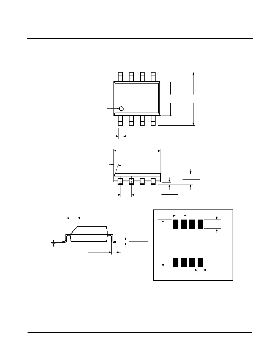
PACKAGING INFORMATION
NOTE:
1. ALL DIMENSIONS IN INCHES (IN PARENTHESES IN MILLIMETERS)
2. PACKAGE DIMENSIONS EXCLUDE MOLDING FLASH
0.020 (0.51)
0.016 (0.41)
0.150 (3.81)
0.125 (3.18)
0.110 (2.79)
0.090 (2.29)
0.430 (10.92)
0.360 (9.14)
0.300
(7.62) REF.
PIN 1 INDEX
0.145 (3.68)
0.128 (3.25)
0.025 (0.64)
0.015 (0.38)
PIN 1
SEATING
PLANE
0.065 (1.65)
0.045 (1.14)
0.260 (6.60)
0.240 (6.10)
0.060 (1.52)
0.020 (0.51)
TYP .0.010 (0.25)
0∞
15∞
8-LEAD PLASTIC DUAL IN-LINE PACKAGE TYPE P
HALF SHOULDER WIDTH ON
ALL END PINS OPTIONAL
0.015 (0.38)
MAX.
0.325 (8.25)
0.300 (7.62)
X25138
13
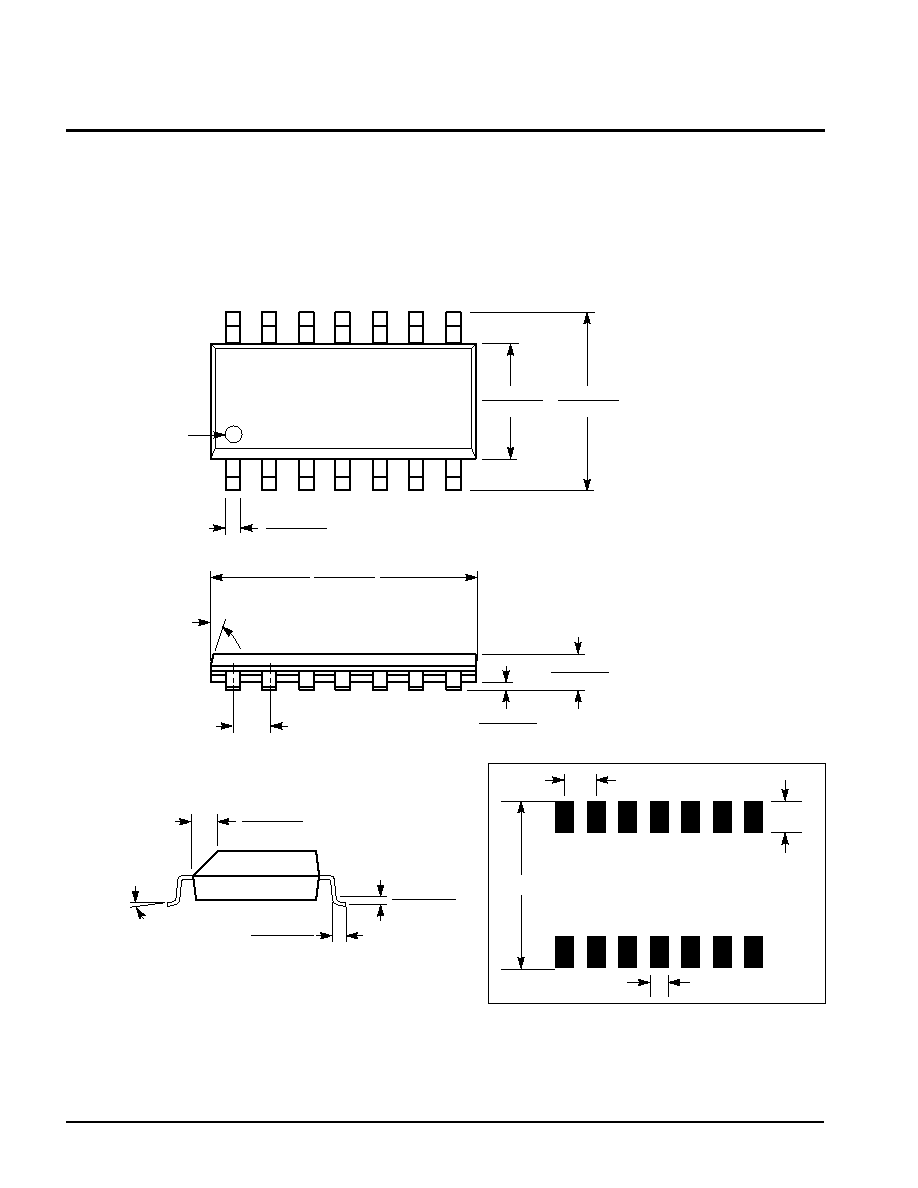
0.150 (3.80)
0.158 (4.00)
0.228 (5.80)
0.244 (6.20)
0.014 (0.35)
0.019 (0.49)
PIN 1
PIN 1 INDEX
0.010 (0.25)
0.020 (0.50)
0.050 (1.27)
0.188 (4.78)
0.197 (5.00)
0.004 (0.19)
0.010 (0.25)
0.053 (1.35)
0.069 (1.75)
(4X) 7
∞
0.016 (0.410)
0.037 (0.937)
0.0075 (0.19)
0.010 (0.25)
0
∞
≠ 8
∞
X 45
∞
8-LEAD PLASTIC SMALL OUTLINE GULL WING PACKAGE TYPE S
0.250"
0.050" TYPICAL
0.050"
TYPICAL
0.030"
TYPICAL
8 PLACES
FOOTPRINT
NOTE: ALL DIMENSIONS IN INCHES (IN PARENTHESES IN MILLIMETERS)
X25138
14
0.150 (3.80)
0.158 (4.00)
0.228 (5.80)
0.244 (6.20)
0.014 (0.35)
0.020 (0.51)
PIN 1
PIN 1 INDEX
0.050 (1.27)
0.336 (8.55)
0.345 (8.75)
0.004 (0.10)
0.010 (0.25)
0.053 (1.35)
0.069 (1.75)
(4X) 7∞
14-LEAD PLASTIC SMALL OUTLINE GULL WING PACKAGE TYPE S
NOTE: ALL DIMENSIONS IN INCHES (IN PARENTHESES IN MILLIMETERS)
0.250"
0.050"
T
ypical
0.050"
T
ypical
0.030"
T
ypical
14 Places
FOO
TPRINT
0.010 (0.25)
0.020 (0.50)
0.016 (0.410)
0.037 (0.937)
0.0075 (0.19)
0.010 (0.25)
0∞ ≠ 8∞
X 45∞
PACKAGING INFORMATION
X25138
15
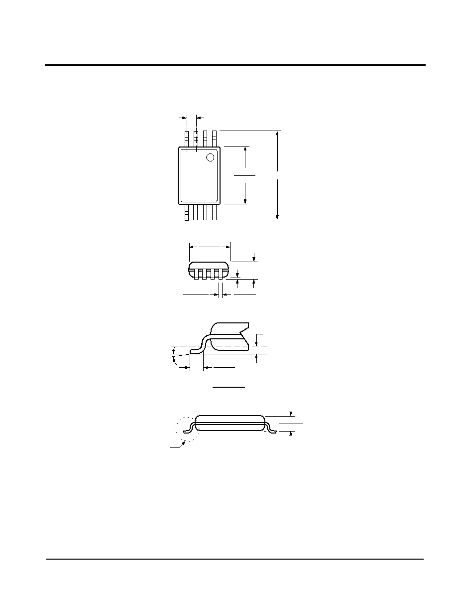
NOTE:
ALL DIMENSIONS IN INCHES (IN PARENTHESES IN MILLIMETERS)
8-LEAD PLASTIC, TSSOP, PACKAGE TYPE V
See Detail "A"
.031 (.80)
.041 (1.05)
.169 (4.3)
.177 (4.5)
.252 (6.4) BSC
.025 (.65) BSC
.114 (2.9)
.122 (3.1)
.002 (.05)
.006 (.15)
.047 (1.20)
.0075 (.19)
.0118 (.30)
0
∞
≠ 8
∞
.010 (.25)
.019 (.50)
.029 (.75)
Gage Plane
Seating Plane
Detail A (20X)
X25138
16
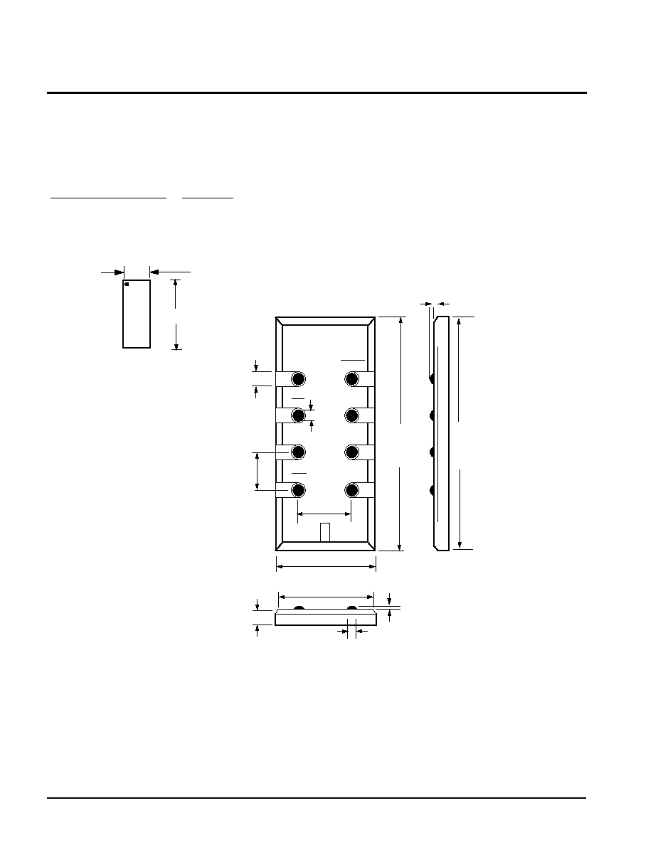
PACKAGING INFORMATION
8-Lead XBGA
ALL DIMENSIONS IN
m
M
ALL DIMENSIONS ARE TYPICAL VALUES
X25138: Bottom View
8-Lead XBGA: Top View
S0
SI
WP
SCK
V
CC
V
SS
CS
HOLD
8
7
6
5
1
2
3
4
.238"
.078"
8-Lead XBGA
Complete Part Number
Top Mark
X25138Z-2.5
XAAD
X25138ZI-2.5
XACR
1200±30
500±20
1000±30
430±50
1982±30
1833±30
6046±30
6046±30
350±20
S0
CS
V
SS
WP
HOLD
V
CC
SI
SCK
215±30
215±30
350±20
PIN 1
X25138
17
ORDERING INFORMATION
PART MARK CONVENTION
X25138
P
-V
Device
V
CC
Limits
Blank = 4.5V to 5.5V
Temperature Range
Blank = Commercial = 0
∞
C to +70
∞
C
Package
LIMITED WARRANTY
Devices sold by Xicor, Inc. are covered by the warranty and patent indemnification provisions appearing in its Terms of Sale only. Xicor, Inc.
makes no warranty, express, statutory, implied, or by description regarding the information set forth herein or regarding the freedom of the
described devices from patent infringement. Xicor, Inc. makes no warranty of merchantability or fitness for any purpose. Xicor, Inc. reserves the
right to discontinue production and change specifications and prices at any time and without notice.
Xicor, Inc. assumes no responsibility for the use of any circuitry other than circuitry embodied in a Xicor, Inc. product. No other circuits, patents,
licenses are implied.
U.S. PATENTS
Xicor products are covered by one or more of the following U.S. Patents: 4,263,664; 4,274,012; 4,300,212; 4,314,265; 4,326,134; 4,393,481;
4,404,475; 4,450,402; 4,486,769; 4,488,060; 4,520,461; 4,533,846; 4,599,706; 4,617,652; 4,668,932; 4,752,912; 4,829, 482; 4,874, 967;
4,883, 976. Foreign patents and additional patents pending.
LIFE RELATED POLICY
In situations where semiconductor component failure may endanger life, system designers using this product should design the system with
appropriate error detection and correction, redundancy and back-up features to prevent such an occurence.
Xicor's products are not authorized for use in critical components in life support devices or systems.
1. Life support devices or systems are devices or systems which, (a) are intended for surgical implant into the body, or (b) support or sustain
life, and whose failure to perform, when properly used in accordance with instructions for use provided in the labeling, can be reasonably
expected to result in a significant injury to the user.
2. A critical component is any component of a life support device or system whose failure to perform can be reasonably expected to cause the
failure of the life support device or system, or to affect its safety or effectiveness.
Z = 8-Lead XBGA
S14 = 14-Lead SOIC
T
P = 8-Lead DIP
2.5 = 2.5 to 5.5V
S8 = 8-Lead SOIC
8-Lead TSSOP
AA = 4.5 to 5.5V, -20 to +85∞C
EYWW
5138XX
AC = 2.5 to 5.5V, -20 to +85∞C
F = 2.5 to 5.5V, 0 to +70∞C
G = 2.5 to 5.5V, -40 to +85∞C
Blank = 4.5 to 5.5V, 0 to +70∞C
I = 4.5 to 5.5V, -40 to +85∞C
8-Lead SOIC/PDIP
X5138 X
XX
Blank = 8-Lead SOIC
F = 2.5 to 5.5V, 0 to +70∞C
G = 2.5 to 5.5V, -40 to +85∞C
Blank = 4.5 to 5.5V, 0 to +70∞C
I = 4.5 to 5.5V, -40 to +85∞C
P = 8-Lead PDIP
AA = 4.5 to 5.5V, -20 to +85∞C
AC = 2.5 to 5.5V, -20 to +85∞C
8-Lead XBGA
Complete Part Number
Top Mark
X25138Z-2.5
XAAD
X25138ZI-2.5
XACR
V8 = 8-Lead TSSOP
I = Industrial = ≠40
∞
C to +85
∞
C

X25138
18
U.S. SALES OFFICES
Corporate Office
Xicor Inc.
1511 Buckeye Drive
Milpitas, CA 95035
Phone: 408/432-8888
Fax: 408/432-0640
E-mail: info@xicor.com
Southeast Region
Xicor Inc.
100 E. Sybelia Ave.
Suite 355
Maitland, FL 32751
Phone: 407/740-8282
Fax: 407/740-8602
E-mail: xicor-se@xicor.com
Mid-Atlantic Region
Xicor Inc.
50 North Street
Danbury, CT 06810
Phone: 203/743-1701
Fax: 203/794-9501
E-mail: xicor-ma@xicor.com
North Central Region
Xicor Inc.
810 South Bartlett Road
Suite 103
Streamwood, IL 60107
Phone: 630/372-3200
Fax: 630/372-3210
E-mail: xicor-nc@xicor.com
South Central Region
Xicor Inc.
11884 Greenville Ave.
Suite 102
Dallas, TX 75243
Phone: 972/669-2022
Fax: 972/644-5835
E-mail: xicor-sc@xicor.com
Southwest Region
Xicor Inc.
4100 Newport Place Drive
Suite 710
Newport Beach, CA 92660
Phone: 714/752-8700
Fax: 714/752-8634
E-mail: xicor-sw@xicor.com
Northwest Region
Xicor Inc.
3333 Bowers Ave.
Suite 238
Santa Clara, CA 95054
Phone: 408/492-1966
Fax: 408/980-9478
E-mail: xicor-nw@xicor.com
INTERNATIONAL SALES OFFICES
EUROPE
Northern Europe
Xicor Ltd.
Grant Thornton House
Witan Way
Witney
Oxford OX8 6FE
UK
Phone: (44) 1933.700544
Fax: (44) 1933.700533
E-mail: xicor-uk@xicor.com
Central Europe
Xicor GmbH
Technopark Neukeferloh
Bretonischer Ring 15
85630 Grasbrunn bei Muenchen
Germany
Phone: (49) 8946.10080
Fax: (49) 8946.05472
E-mail: xicor-gm@xicor.com
ASIA/PACIFIC
Japan
Xicor Japan K.K.
Suzuki Building, 4th Floor
1-6-8 Shinjuku, Shinjuku-ku
Tokyo 160, Japan
Phone: (81) 3322.52004
Fax: (81) 3322.52319
E-mail: xicor-jp@xicor.com
Mainland China
Taiwan/Hong Kong
Xicor Hong Kong, Ltd.
Room 7, Business Centre
B1, Grand Stanford Harbour View
70 Mody Road, Tsimshatsui East
Kowloon, Hong Kong
Phone: (852) 2313 7607
Fax: (852) 2313 7507
E-mail: xicor_hongkong@xicor.com
Singapore/Malaysia/India
Xicor Inc.
3333 Bowers Ave.
Suite 238
Santa Clara, CA 95054
Phone: 408/492-1966
Fax: 408/980-9478
E-mail: xicor-nw@xicor.com
Korea
Xicor Korea, Ltd.
27th Fl., Korea World Trade Ctr.
159, Samsung-dong
Kangnam Ku
Seoul 135-729
Korea
Phone: (82) 2.551.2750
Fax: (82) 2.551.2710
E-mail: xicor-ka@xicor.com
( ) = Country Code
Xicor, Inc., Marketing Dept. 1511 Buckeye Drive, Milpitas, California 95035-7493 TEL 408/432-8888 FAX 408/432-0640
Xicor product information is available at:
www.xicor.com