For a more
Integrated Solution use
Xicor System Management Products
REV 1.2 11/28/00
Characteristics subject to change without notice.
1 of 14
www.xicor.com
Recommended System Management
Alternative: X5163
16K
X25160
2K x 8 Bit
SPI Serial EEPROM With Block Lock
TM
Protection
FEATURES
� 2MHz clock rate
� SPI modes (0,0 & 1,1)
� 2K X 8 bits
--32-byte page mode
� Low power CMOS
--<1�A standby current
--<5mA active current
� 2.7V To 5.5V power supply
� Block lock protection
--Protect 1/4, 1/2 or all of EEPROM array
� Built-in inadvertent write protection
--Power-up/power-down protection circuitry
--Write enable latch
--Write protect pin
� Self-timed write cycle
--5ms write cycle time (typical)
� High reliability
--Endurance: 1,000,000 cycles
--Data retention: 100 years
--ESD protection: 2000V on all pins
� 8-lead PDlP package
� 8-lead SOIC package
DESCRIPTION
The X25160 is a CMOS 16384-bit serial EEPROM,
internally organized as 2K x 8. The X25160 features a
Serial Peripheral Interface (SPI) and software proto-
col, allowing operation on a simple three-wire bus. The
bus signals are a clock input (SCK) plus separate data
in (SI) and data out (SO) lines. Access to the device is
controlled through a chip select (CS) input, allowing
any number of devices to share the same bus.
The X25160 also features two additional inputs that
provide the end user with added flexibility. By assert-
ing the HOLD input, the X25160 will ignore transitions
on its inputs, thus allowing the host to service higher
priority interrupts. The WP input can be used as a
hardwire input to the X25160 disabling all write
attempts to the status register, thus providing a mech-
anism for limiting end user capability of altering 0, 1/4,
1/2 or all of the memory.
The X25160 utilizes Xicor's proprietary Direct Write
TM
cell, providing a minimum endurance of 1,000,000
cycles and a minimum data retention of 100 years.
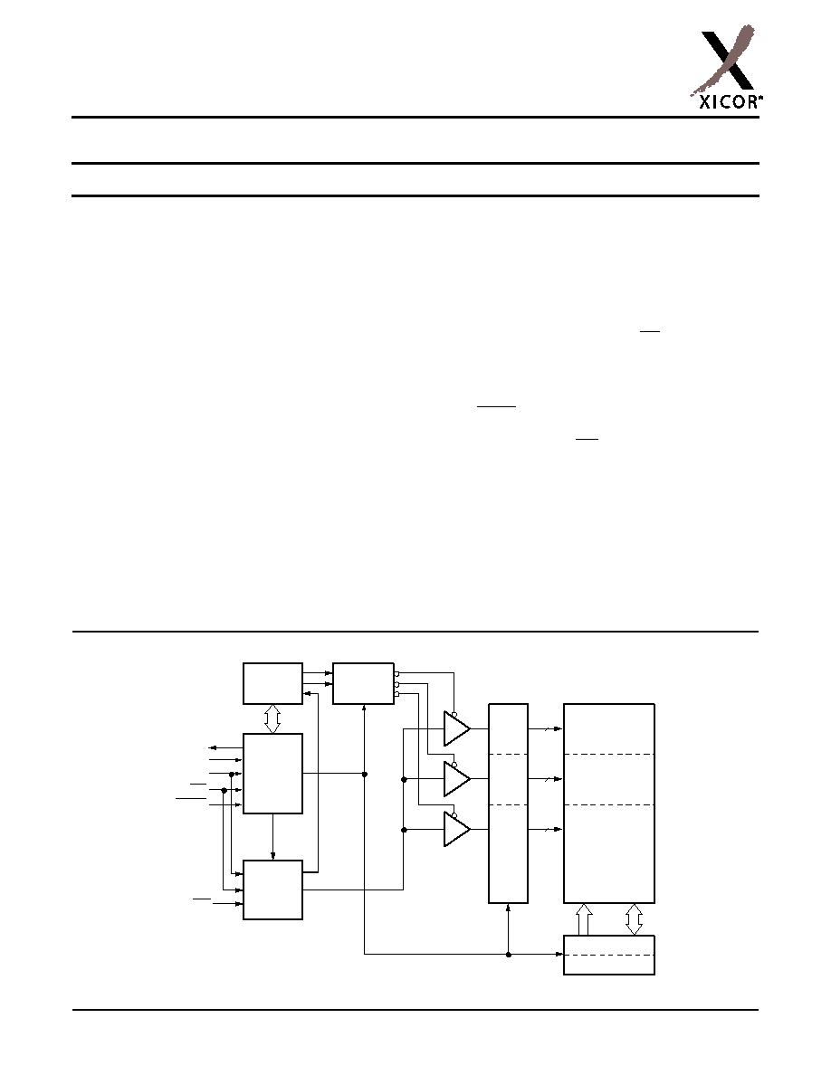
BLOCK DIAGRAM
Command
Decode
and
Control
Logic
Write
Control
and
Timing
Logic
Write
Protect
Logic
X Decode
Logic
2K Byte
Array
16 X 256
Y Decode
Data Register
SO
SI
SCK
CS
HOLD
WP
16
32
8
32
Status
Register
16
32 X 256
16 X 256
Direct Write
TM
and Block Lock
TM
Protection is a trademark of Xicor, Inc.
For a more
Integrated Solution use
Xicor System Management Products
X25160
Characteristics subject to change without notice.
2 of 14
REV 1.2 11/28/00
www.xicor.com
PIN DESCRIPTIONS
Serial Output (SO)
SO is a push/pull serial data output pin. During a read
cycle, data is shifted out on this pin. Data is clocked out
by the falling edge of the serial clock.
Serial Input (SI)
SI is the serial data input pin. All opcodes, byte
addresses, and data to be written to the memory are
input on this pin. Data is latched by the rising edge of
the serial clock.
Serial Clock (SCK)
The Serial Clock controls the serial bus timing for data
input and output. Opcodes, addresses, or data present
on the SI pin are latched on the rising edge of the clock
input, while data on the SO pin change after the falling
edge of the clock input.
Chip Select (CS)
It should be noted that after power-up, a HIGH to LOW
transition on CS is required prior to the start of any
operation.
When CS is HIGH, the X25160 is deselected, the SO
output pin is at HIGH impedance and, unless an inter-
nal write operation is underway, the X25160 will be in
the standby power mode. CS LOW enables the
X25160, placing it in the active power mode.
Write Protect (WP)
When WP is LOW and the nonvolatile bit WPEN is "1",
nonvolatile writes to the X25160 status register are dis-
abled, but the part otherwise functions normally. When
WP is held HIGH, all functions, including nonvolatile
writes operate normally. WP going LOW while CS is
still LOW will interrupt a write to the X25160 status reg-
ister. If the internal write cycle has already been initi-
ated, WP going LOW will have no effect on a write.
The WP pin function is blocked when the WPEN bit in
the status register is "0". This allows the user to install
the X25160 in a system with WP pin grounded, and still
be able to write to the status register. The WP pin func-
tions will be enabled when the WPEN bit is set "1".
Hold (HOLD)
HOLD is used in conjunction with the CS pin to select
the device. Once the part is selected and a serial
sequence is underway, HOLD may be used to pause
the serial communication with the controller without
resetting the serial sequence. To pause, HOLD must
be brought LOW while SCK is LOW. To resume com-
munication, HOLD is brought HIGH, again while SCK
is LOW. If the pause feature is not used, HOLD should
be held HIGH at all times.
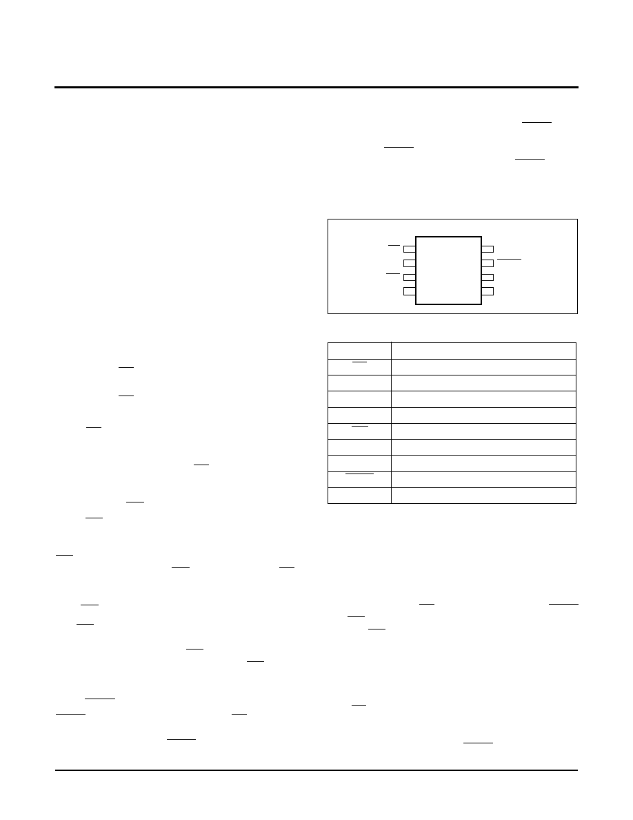
PIN CONFIGURATION
n
PIN NAMES
PRINCIPLES OF OPERATION
The X25160 is a 2K x 8 EEPROM designed to interface
directly with the synchronous serial peripheral interface
(SPI) of many popular microcontroller families.
The X25160 contains an 8-bit instruction register. It is
accessed via the SI input, with data being clocked in
on the rising SCK. CS must be LOW and the HOLD
and WP inputs must be HIGH during the entire opera-
tion. The WP input is "Don't Care" if WPEN is set "0".
Table 1 contains a list of the instructions and their
opcodes. All instructions, addresses and data are
transferred MSB first.
Data input is sampled on the first rising edge of SCK
after CS goes LOW. SCK is static, allowing the user to
stop the clock and then resume operations. If the clock
line is shared with other peripheral devices on the SPI
bus, the user can assert the HOLD input to place the
Symbol
Description
CS
Chip Select Input
SO
Serial Output
SI
Serial Input
SCK
Serial Clock Input
WP
Write Protect Input
V
SS
Ground
V
CC
Supply Voltage
HOLD
Hold Input
NC
No Connect
DIP/SOIC
X25160
CS
SO
WP
V
SS
1
2
3
4
8
7
6
5
V
CC
HOLD
SCK
SI
For a more
Integrated Solution use
Xicor System Management Products
X25160
Characteristics subject to change without notice.
3 of 14
REV 1.2 11/28/00
www.xicor.com
X25160 into a "PAUSE" condition. After releasing
HOLD, the X25160 will resume operation from the
point when HOLD was first asserted.
Write Enable Latch
The X25160 contains a "write enable" latch. This latch
must be SET before a write operation will be com-
pleted internally. The WREN instruction will set the
latch and the WRDI instruction will reset the latch. This
latch is automatically reset upon a power-up condition
and after the completion of a byte, page, or status reg-
ister write cycle.
Status Register
The RDSR instruction provides access to the status
register. The status register may be read at any time,
even during a write cycle. The status register is format-
ted as follows:
WPEN, BP0 and BP1 are set by the WRSR instruction.
WEL and WIP are read-only and automatically set by
other operations.
The Write-In-Process (WIP) bit indicates whether the
X25160 is busy with a write operation. When set to a
"1", a write is in progress, when set to a "0", no write is
in progress. During a write, all other bits are set to "1".
The Write Enable Latch (WEL) bit indicates the status
of the "write enable" latch. When set to a "1", the latch
is set, when set to a "0", the latch is reset.
The Block Protect (BP0 and BP1) bits are nonvolatile
and allow the user to select one of four levels of protec-
tion. The X25160 is divided into four 4096-bit segments.
One, two, or all four of the segments may be protected.
That is, the user may read the segments but will be
unable to alter (write) data within the selected seg-
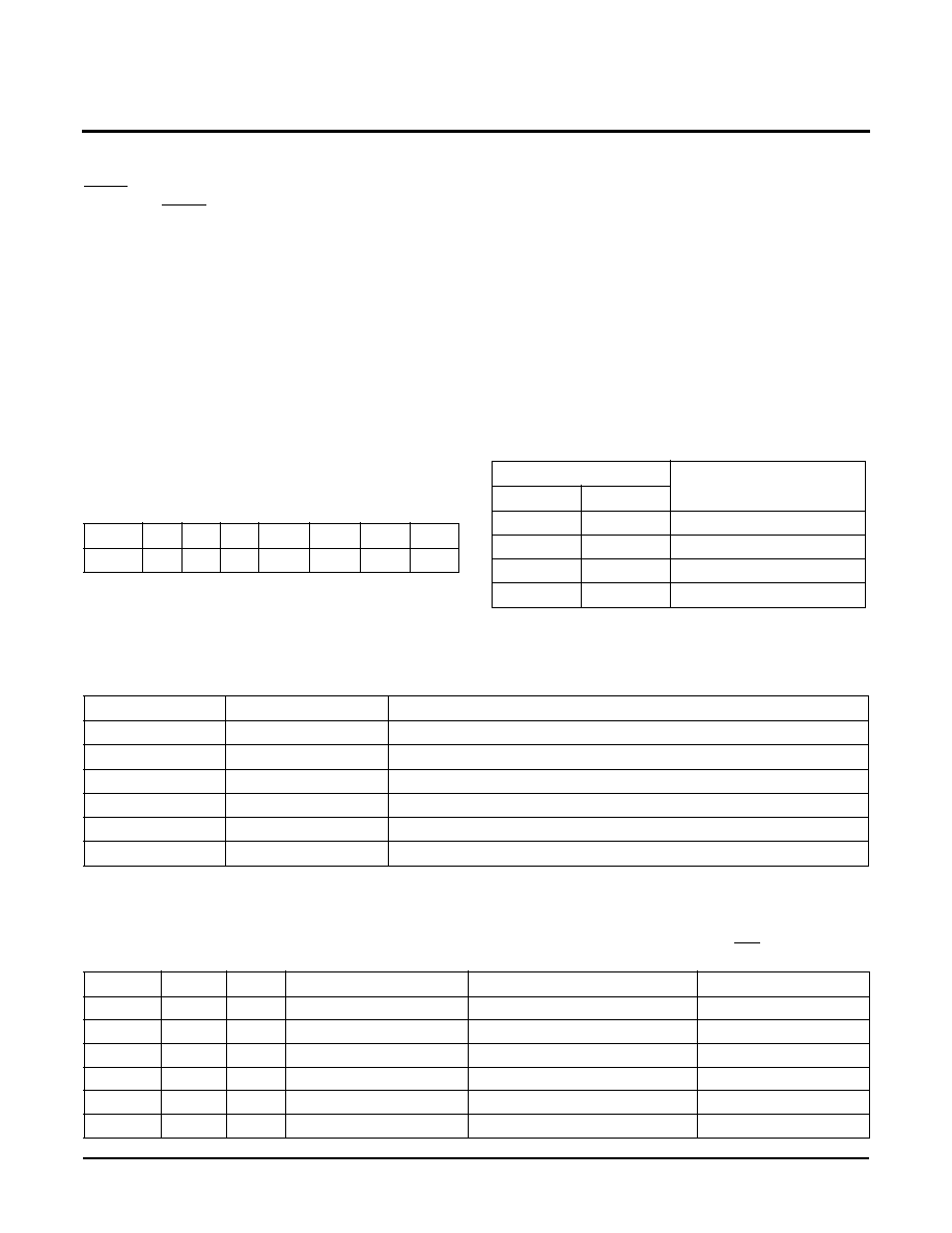
ments. The partitioning is controlled as illustrated below.
7
6
5
4
3
2
1
0
WPEN
X
X
X
BP1
BP0
WEL
WIP
Status Register Bits
Array Addresses
Protected
BP1
BP0
0
0
None
0
1
$0600�$07FF
1
0
$0400�$07FF
1
1
$0000�$07FF
Table 1. Instruction Set
Note:
*Instructions are shown MSB in leftmost position. Instructions are transferred MSB first.
Write-Protect Enable
The Write-Protect-Enable (WPEN) is available for the X25160 as a nonvolatile enable bit for the WP pin.
Instruction Name
Instruction Format*
Operation
WREN
0000 0110
Set the write enable latch (enable write operations)
WRDI
0000 0100
Reset the write enable latch (disable write operations)
RDSR
0000 0101
Read status register
WRSR
0000 0001
Write status register
READ
0000 0011
Read data from memory array beginning at selected address
WRITE
0000 0010
Write data to memory array beginning at selected address (1 to 32-bytes)
WPEN
WP
WEL
Protected Blocks
Unprotected Blocks
Status Register
0
X
0
Protected
Protected
Protected
0
X
1
Protected
Writable
Writable
1
Low
0
Protected
Protected
Protected
1
Low
1
Protected
Writable
Protected
X
High
0
Protected
Protected
Protected
X
High
1
Protected
Writable
Writable

For a more
Integrated Solution use
Xicor System Management Products
X25160
Characteristics subject to change without notice.
4 of 14
REV 1.2 11/28/00
www.xicor.com
The Write Protect (WP) pin and the nonvolatile Write
Protect Enable (WPEN) bit in the status register control
the programmable hardware write protect feature.
Hardware write protection is enabled when WP pin is
LOW, and the WPEN bit is "1". Hardware write protec-
tion is disabled when either the WP pin is HIGH or the
WPEN bit is "0". When the chip is hardware write pro-
tected, nonvolatile writes are disabled to the status reg-
ister, including the block protect bits and the WPEN bit
itself, as well as the block-protected sections in the
memory array. Only the sections of the memory array
that are not block-protected can be written.
Note:
Since the WPEN bit is write protected, it cannot
be changed back to a "0", as long as the WP pin is held
LOW.
Clock and Data Timing
Data input on the SI line is latched on the rising edge
of SCK. Data is output on the SO line by the falling
edge of SCK.
Read Sequence
When reading from the EEPROM memory array, CS is
first pulled LOW to select the device. The 8-bit read
instruction is transmitted to the X25160, followed by
the 16-bit address, of which the last 11 are used. After
the read opcode and address are sent, the data stored
in the memory at the selected address is shifted out on
the SO line. The data stored in memory at the next
address can be read sequentially by continuing to pro-
vide clock pulses. The address is automatically incre-
mented to the next higher address after each byte of
data is shifted out. When the highest address is
reached ($07FF) the address counter rolls over to
address $0000 allowing the read cycle to be continued
indefinitely. The read operation is terminated by taking
CS HIGH. Refer to the read EEPROM array operation
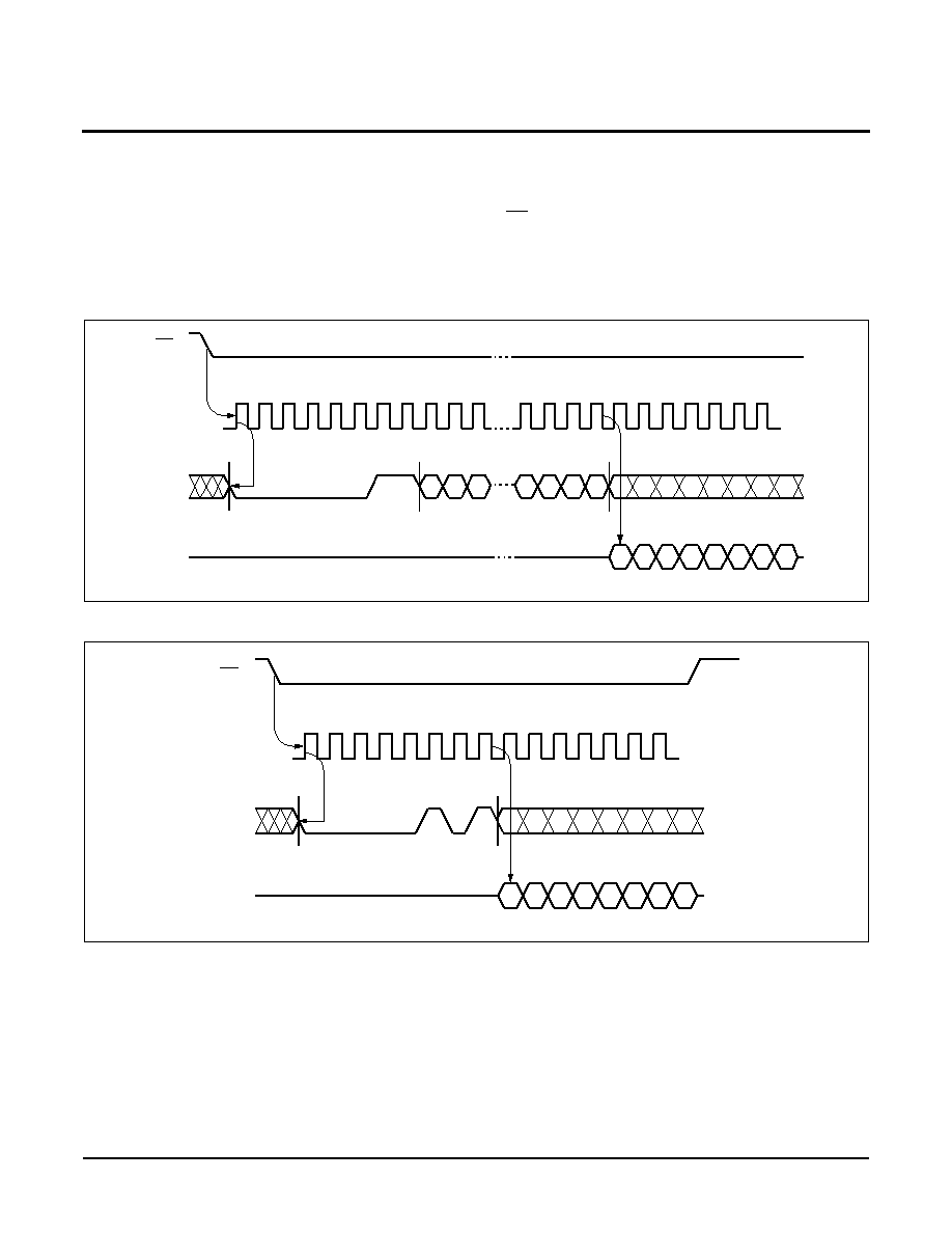
sequence illustrated in Figure 1.
To read the status register the CS line is first pulled
LOW to select the device followed by the 8-bit RDSR
instruction. After the RDSR opcode is sent, the con-
tents of the status register are shifted out on the SO
line. The read status register sequence is illustrated in
Figure 2.
Write Sequence
Prior to any attempt to write data into the X25160, the
"write enable" latch must first be set by issuing the WREN
instruction (See Figure 3). CS is first taken LOW, then the
WREN instruction is clocked into the X25160. After all
eight bits of the instruction are transmitted, CS must then
be taken HIGH. If the user continues the write operation
without taking CS HIGH (after issuing the WREN
instruction), the write operation will be ignored.
To write data to the EEPROM memory array, the user
issues the write instruction, followed by the address
and then the data to be written. This is minimally a
thirty-two clock operation. CS must go LOW and
remain LOW for the duration of the operation. The host
may continue to write up to 32-bytes of data to the
X25160. The only restriction is the 32-bytes must reside
on the same page. If the address counter reaches the
end of the page and the clock continues, the counter will
"roll over" to the first address of the page and overwrite
any data that may have been written.
For the write operation (byte or page write) to be com-
pleted, CS can only be brought HIGH after bit 0 of data
byte N is clocked in. If it is brought HIGH at any other
time the write operation will not be completed. Refer to
Figures 4 and 5 for a detailed illustration of the write
sequences and time frames in which CS going HIGH
are valid.
To write to the status register, the WRSR instruction is
followed by the data to be written. Data bits 0, 1, 4, 5
and 6 must be "0". This sequence is shown in Figure 6.
While the write is in progress following a status register
or EEPROM write sequence, the status register may
be read to check the WIP bit. During this time the WIP
bit will be HIGH.
Hold Operation
The HOLD input should be HIGH (at V
IH
) under normal
operation. If a data transfer is to be interrupted, HOLD
can be pulled LOW to suspend the transfer until it can
be resumed. The only restriction is the SCK input must
be LOW when HOLD is first pulled LOW, and SCK
must also be LOW when HOLD is released.
The HOLD input may be tied HIGH either directly to
V
CC
or tied to V
CC
through a resistor.
Operational Notes
The X25160 powers-up in the following state:
� The device is in the LOW power standby state.
� A HIGH to LOW transition on CS is required to enter
an active state and receive an instruction.
� SO pin is HIGH impedance.
� The "write enable" latch is reset.
For a more
Integrated Solution use
Xicor System Management Products
X25160
Characteristics subject to change without notice.
5 of 14
REV 1.2 11/28/00
www.xicor.com
Data Protection
The following circuitry has been included to prevent
inadvertent writes:
� The "write enable" latch is reset upon power-up.
� A WREN instruction must be issued to set the "write
enable" latch.
� CS must come HIGH at the proper clock count in
order to start a write cycle.
Figure 1. Read EEPROM Array Operation Sequence
Figure 2. Read Status Register Operation Sequence
0
1
2
3
4
5
6
7
8
9
10
20 21 22 23 24 25 26 27 28 29 30
7
6
5
4
3
2
1
0
Data Out
CS
SCK
SI
SO
MSB
High Impedance
Instruction
16 Bit Address
15 14 13
3
2
1
0
0
1
2
3
4
5
6
7
8
9
10 11
12 13 14
7
6
5
4
3
2
1
0
CS
SCK
SI
SO
MSB
High Impedance
Instruction
Data Out