Document Outline
- Table of Contents
- Product Selection
- Data Sheet Alpha
- Ap Note Alpha
©
Xicor, Inc. 1994, 1995, 1996 Patents Pending
7050 -1.0 6/20/97 T0/C0/D0 SH
1
Characteristics subject to change without notice
64K
32K
16K
X25644/46
X25324/26
X25164/66
8K x 8 Bit
4K x 8 Bit
2K x 8 Bit
Programmable Watchdog Timer w/Serial E
2
PROM
FEATURES
∑ Programmable Watchdog Timer with Reset
Assertion
--Reset Signal Valid to Vcc=1V
--Power Up Reset Control
∑ Save Critical Data With Block Lock
TM
Protection
--Block Lock
TM
Protect 0, 1/4, 1/2 or all of
Serial E
2
PROM Memory Array
∑ In Circuit Programmable ROM Mode
∑ Long Battery Life With Low Power Consumption
--<50
µ
A Max Standby Current, Watchdog On
--<1
µ
A Max Standby Current, Watchdog Off
--<5mA Max Active Current during Write
--<400
µ
A Max Active Current during Read
∑ 1.8V to 3.6V, 2.7V to 5.5V and 4.5V to 5.5V Power
Supply Operation
∑ 2MHz Clock Rate
∑ Minimize Programming Time
--32 Byte Page Write Mode
--Self-Timed Write Cycle
--5ms Write Cycle Time (Typical)
∑ SPI Modes (0,0 & 1,1)
∑ Built-in Inadvertent Write Protection
--Power-Up/Power-Down Protection Circuitry
--Write Enable Latch
--Write Protect Pin
∑ High Reliability
∑ Available Packages
--14-Lead SOIC (X2564x)
--14-Lead TSSOP (X2532x, X2516x)
--8-Lead SOIC (X2532x, X2516x)
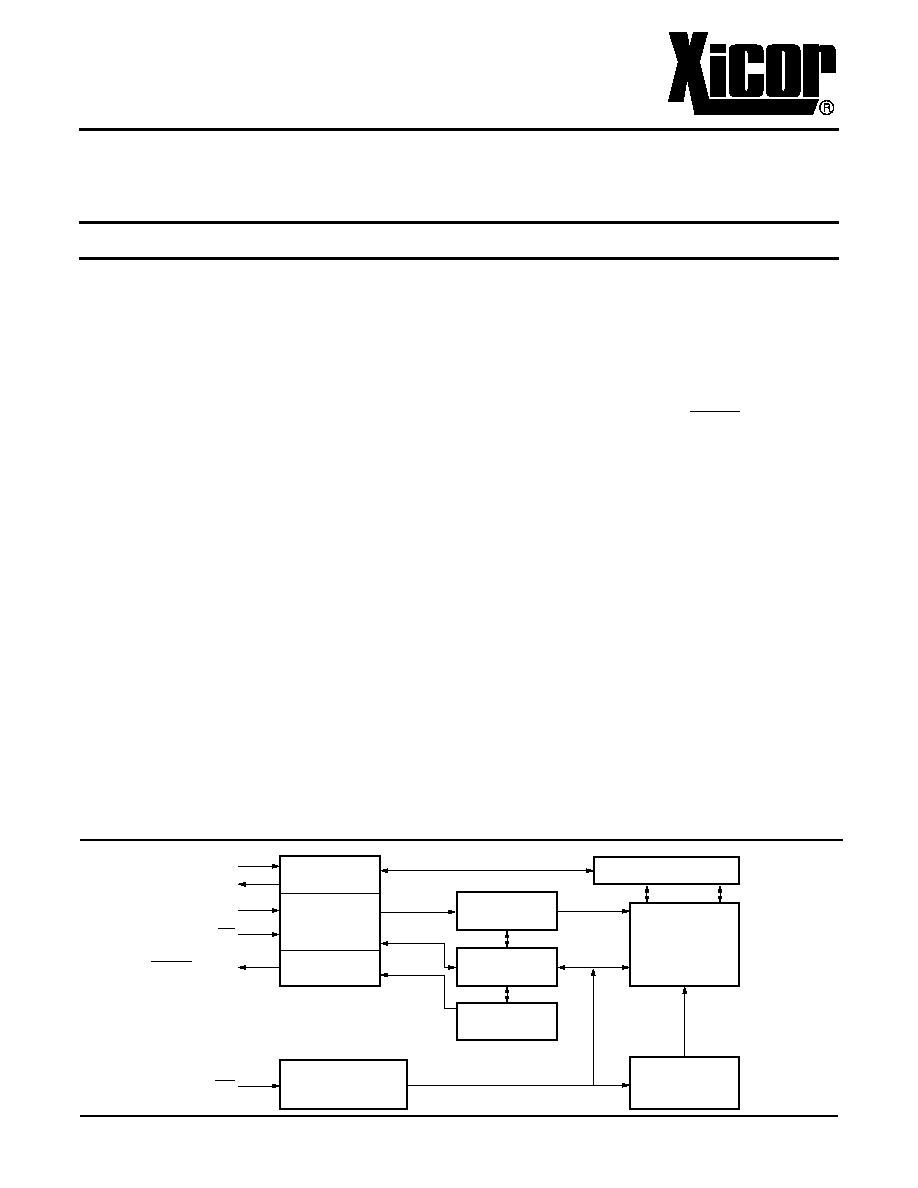
DESCRIPTION
These devices combine two popular functions, Watchdog
Timer, and Serial E
2
PROM Memory in one package. This
combination lowers system cost, reduces board space
requirements, and increases reliability.
The Watchdog Timer provides an independent protection
mechanism for microcontrollers. During a system failure,
the device will respond with a RESET/RESET signal
after a selectable time-out interval. The user selects the
interval from three preset values. Once selected, the
interval does not change, even after cycling the power.
The memory portion of the device is a CMOS Serial
E
2
PROM array with Xicor's Block Lock
TM
Protection. The
array is internally organized as x 8. The device features a
Serial Peripheral Interface (SPI) and software protocol
allowing operation on a simple four-wire bus.
The device utilizes Xicor's proprietary Direct Write
TM
cell,
providing a minimum endurance of 100,000 cycles per
sector and a minimum data retention of 100 years.
BLOCK DIAGRAM
DATA
REGISTER
COMMAND
DECODE &
CONTROL
LOGIC
RESET
CONTROL
WRITE,
BLOCK LOCK &
ICP ROM CONTROL
X - DECODE
LOGIC
STATUS
REGISTER
WATCHDOG
PAGE DECODE LOGIC
SERIAL
E
2
PROM
ARRAY
HIGH
VOLTAGE
CONTROL
SI
SO
SCK
CS
RESET/RESET
WP
7029 FRM 01
32
8
TIMER
X25644/46
X25324/26
X25164/66
2
PIN DESCRIPTIONS
Serial Output (SO)
SO is a push/pull serial data output pin. During a read
cycle, data is shifted out on this pin. Data is clocked out by
the falling edge of the serial clock.
Serial Input (SI)
SI is a serial data input pin. All opcodes, byte addresses,
and data to be written to the memory are input on this pin.
Data is latched by the rising edge of the serial clock.
Serial Clock (SCK)
The Serial Clock controls the serial bus timing for data
input and output. Opcodes, addresses, or data present on
the SI pin are latched on the rising edge of the clock input,
while data on the SO pin change after the falling edge of
the clock input.
Chip Select (CS)
When CS is HIGH, the device is deselected and the SO
output pin is at high impedance and unless a nonvolatile
write cycle is underway, the device will be in the standby
power mode. CS LOW enables the device's, placing it in
the active power mode. It should be noted that after
power-up, a HIGH to LOW transition on CS is required
prior to the start of any operation.
Write Protect (WP)
When WP is low and the nonvolatile bit WPEN is "1",
nonvolatile writes to the device's Status Register are
disabled, but the part otherwise functions normally. When
WP is held high, all functions, including nonvolatile writes
to the Status Register operate normally. If an internal
Status Register Write Cycle has already been initiated,
WP going low while WPEN is a "1" will have no effect on
this write. Subsequent write attempts to the Status
Register under these conditions will be disabled.
The WP pin function is blocked when the WPEN bit in the
Status Register is "0". This allows the user to install the
device in a system with WP pin grounded and still be able
to program the Status Register. The WP pin functions will
be enabled when the WPEN bit is set to a "1".
Reset (RESET/RESET)
RESET/RESET is an active LOW/HIGH, open drain out-
put which goes active whenever the Watchdog Timer is
enabled and CS remains either HIGH or LOW longer than
the selectable Watchdog time-out period. It will remain
active for t
RST
, the Reset Timeout period. A falling edge of
CS will reset the Watchdog Timer.
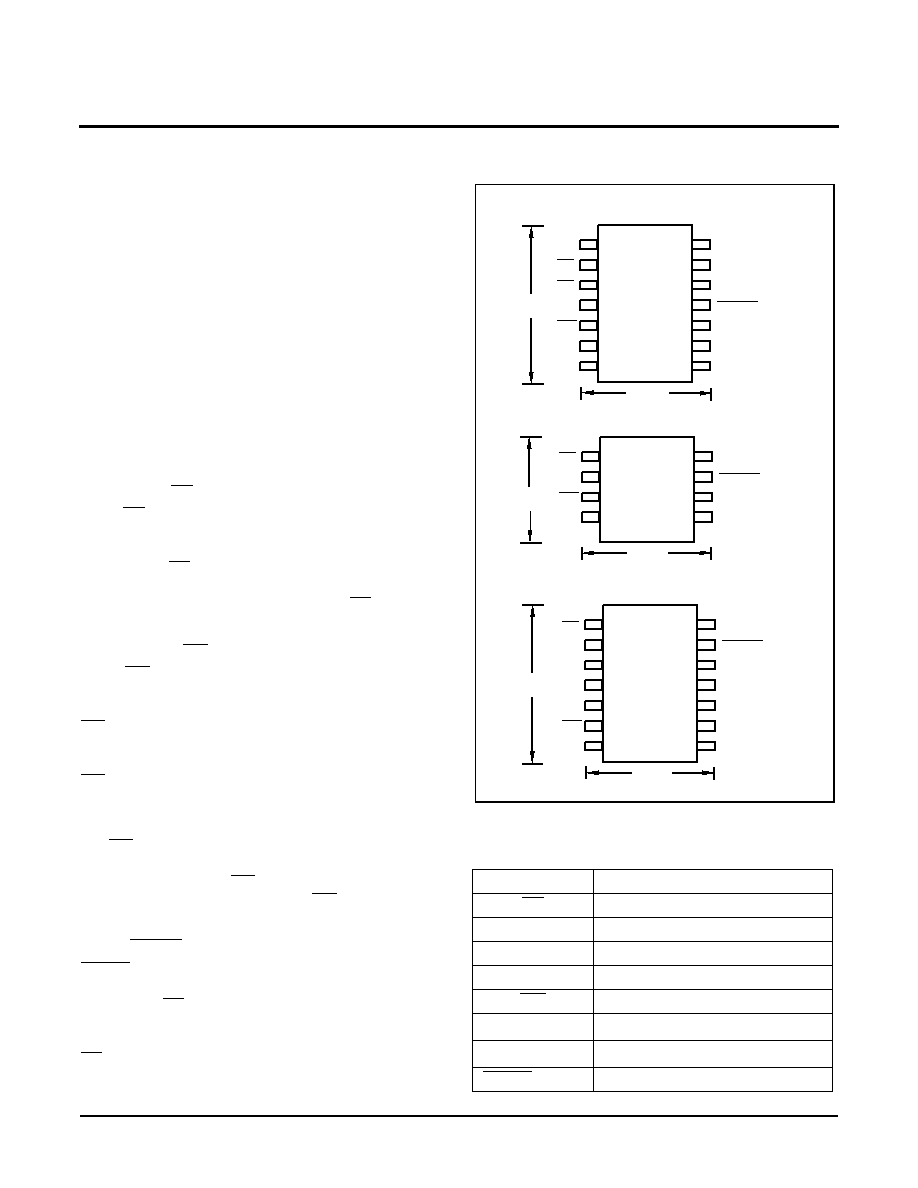
PIN CONFIGURATION
PIN NAMES
7029 FRM T01
Symbol
Description
CS
Chip Select Input
SO
Serial Output
SI
Serial Input
SCK
Serial Clock Input
WP
Write Protect Input
V
SS
Ground
V
CC
Supply Voltage
RESET/RESET
Reset Output
14-LEAD SOIC
X25644/46
NC
CS
CS
SO
WP
VSS
1
2
3
4
5
6
7
RESET/RESET
SCK
SI
NC
14
13
12
11
10
9
8
NC
VCC
VCC
NC
7036 FRM 02
8-LEAD SOIC
X25324/26
CS
WP
SO
1
2
3
4
RESET/RESET
8
7
6
5
VCC
14-LEAD TSSOP
X25324/28
SO
WP
VSS
1
2
3
4
5
6
7
RESET/RESET
SCK
SI
14
13
12
11
10
9
8
NC
VCC
NC
X25164/66
VSS
SCK
SI
CS
NC
NC
NC
NC
X25164/66
0.345"
0.200"
0.197"
0.244"
0.177"
0.244"
Not to Scale
X25644/46
X25324/26
X25164/66
3
PRINCIPLES OF OPERATION
The device is designed to interface directly with the syn-
chronous Serial Peripheral Interface (SPI) of many popu-
lar microcontroller families.
The device monitors the bus and asserts RESET/RESET
output if there is no bus activity within user programmable
time-out period. The device contains an 8-bit instruction
register. It is accessed via the SI input, with data being
clocked in on the rising edge of SCK. CS must be LOW
during the entire operation.
All instructions (Table 1), addresses and data are trans-
ferred MSB first. Data input on the SI line is latched on the
first rising edge of SCK after CS goes LOW. Data is out-
put on the SO line by the falling edge of SCK. SCK is
static, allowing the user to stop the clock and then start it
again to resume operations where left off.
Write Enable Latch
The device contains a Write Enable Latch. This latch must
be SET before a Write Operation is initiated. The WREN
instruction will set the latch and the WRDI instruction will
reset the latch (Figure 3). This latch is automatically reset
upon a power-up condition and after the completion of a
valid Write Cycle.
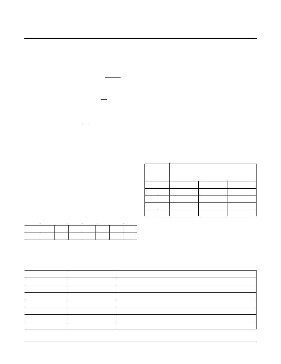
Status Register
The RDSR instruction provides access to the Status Reg-
ister. The Status Register may be read at any time, even
during a Write Cycle. The Status Register is formatted as
follows:
The Write-In-Progress (WIP) bit is a volatile, read only bit
and indicates whether the device is busy with an internal
nonvolatile write operation. The WIP bit is read using the
RDSR instruction. When set to a "1", a nonvolatile write
operation is in progress. When set to a "0", no write is in
progress.
The Write Enable Latch (WEL) bit indicates the Status of
the Write Enable Latch. When WEL=1, the latch is set
HIGH and when WEL=0 the latch is reset LOW. The WEL
bit is a volatile, read only bit. It can be set by the WREN
instruction and can be reset by the WRDI instruction.
The Block Lock bits, BL0 and BL1, set the level of Block
Lock
TM
Protection. These nonvolatile bits are pro-
grammed using the WRSR instruction and allow the user
to protect one quarter, one half, all or none of the
E
2
PROM array. Any portion of the array that is Block Lock
Protected can be read but not written. It will remain pro-
tected until the BL bits are altered to disable Block Lock
Protection of that portion of memory.
7029 FRM T03
7
6
5
4
3
2
1
0
WPEN
FLB
WD1 WD0
BL1
BL0
WEL
WIP
7029 FRM T02
Status
Register
Bits
Array Addresses Protected
BL1 BL0
X2564x
X2532x
X2516x
0
0
None
None
None
0
1
$1800≠$1FFF $0C00≠$0FFF $0600≠$07FF
1
0
$1000≠$1FFF $0800≠$0FFF $0400≠$07FF
1
1
$0000≠$1FFF $0000≠$0FFF $0000≠$07FF
Table 1. Instruction Set
*Instructions are shown MSB in leftmost position. Instructions are transferred MSB first.
7029 FRM T04
Instruction Name
Instruction Format*
Operation
WREN
0000 0110
Set the Write Enable Latch (Enable Write Operations)
SFLB
0000 0000
Set Flag Bit
WRDI/RFLB
0000 0100
Reset the Write Enable Latch/Reset Flag Bit
RSDR
0000 0101
Read Status Register
WRSR
0000 0001
Write Status Register(Watchdog, BlockLock & WPEN Bits)
READ
0000 0011
Read Data from Memory Array Beginning at Selected Address
WRITE
0000 0010
Write Data to Memory Array Beginning at Selected Address
X25644/46
X25324/26
X25164/66
4
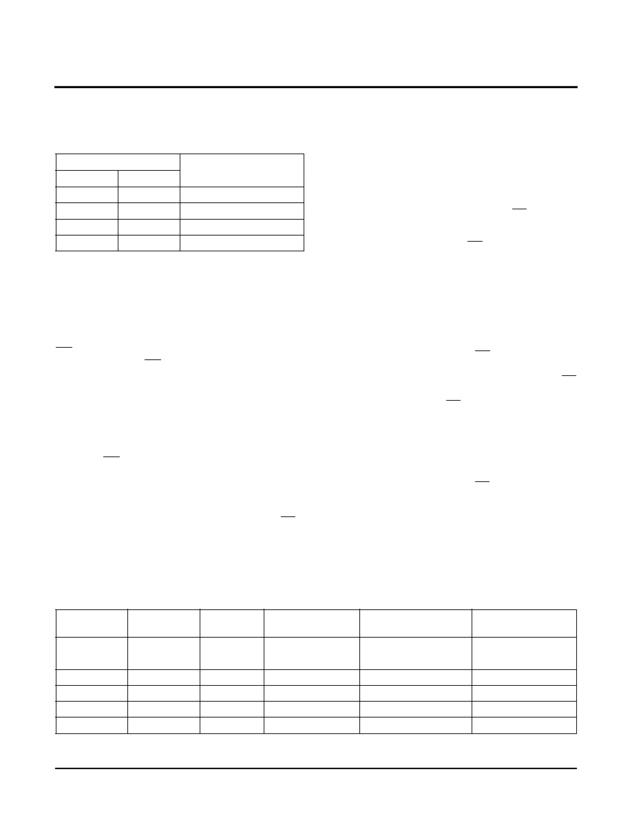
The Watchdog Timer bits, WD0 and WD1, select the
Watchdog Time-out Period. These nonvolatile bits are
programmed with the WRSR instruction.
7029 FRM T05
The FLAG bit shows the status of a volatile latch that can
be set and reset by the system using the SFLB and RFLB
instructions. The Flag bit is automatically reset upon
power up.
The nonvolatile WPEN bit is programmed using the
WRSR instruction. This bit works in conjunction with the
WP pin to provide Programmable Hardware Write Protec-
tion (Table 2). When WP is LOW and the WPEN bit is pro-
grammed HIGH, all Status Register Write Operations are
disabled.
In Circuit Programmable ROM Mode
This mechanism protects the Block Lock and Watchdog
bits from inadvertant corruption. It may be used to per-
form an In Circuit Programmable ROM function by hard-
wiring the WP pin to ground, writing and Block Locking
the desired portion of the array to be ROM, and then pro-
gramming the WPEN bit HIGH.
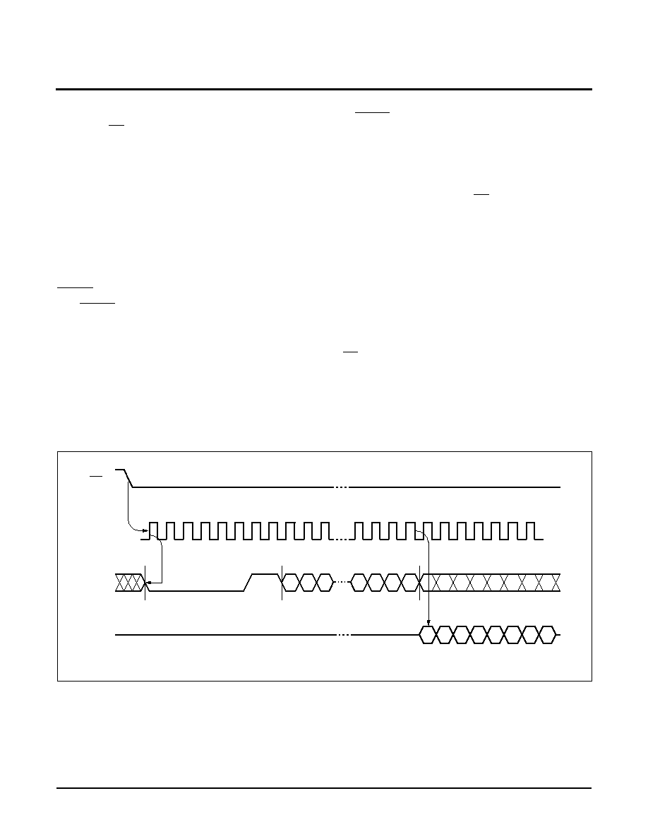
Read Sequence
When reading from the E
2
PROM memory array, CS is
first pulled low to select the device. The 8-bit READ
instruction is transmitted to the device, followed by the 16-
bit address. After the READ opcode and address are
sent, the data stored in the memory at the selected
address is shifted out on the SO line. The data stored in
memory at the next address can be read sequentially by
continuing to provide clock pulses. The address is auto-
matically incremented to the next higher address after
each byte of data is shifted out. When the highest address
is reached, the address counter rolls over to address
$0000 allowing the read cycle to be continued indefinitely.
The read operation is terminated by taking CS high. Refer
to the Read E
2
PROM Array Sequence (Figure 1).
To read the Status Register, the CS line is first pulled low
to select the device followed by the 8-bit RDSR instruc-
tion. After the RDSR opcode is sent, the contents of the
Status Register are shifted out on the SO line. Refer to
the Read Status Register Sequence (Figure 2).
Write Sequence
Prior to any attempt to write data into the device, the
"Write Enable" Latch (WEL) must first be set by issuing
the WREN instruction (Figure 3). CS is first taken LOW,
then the WREN instruction is clocked into the device.
After all eight bits of the instruction are transmitted, CS
must then be taken HIGH. If the user continues the Write
Operation without taking CS HIGH after issuing the
WREN instruction, the Write Operation will be ignored.
To write data to the E
2
PROM memory array, the user then
issues the WRITE instruction followed by the 16 bit
address and then the data to be written. Any unused
address bits are specified to be "0's". The WRITE opera-
tion minimally takes 32 clocks. CS must go low and
remain low for the duration of the operation. If the address
counter reaches the end of a page and the clock contin-
ues, the counter will roll back to the first address of the
page and overwrite any data that may have been previ-
ously written.
Status Register Bits
Watchdog Time-out
(Typical)
WD1
WD0
0
0
1.4 Seconds
0
1
600 Milliseconds
1
0
200 Milliseconds
1
1
Disabled
Table 2. Block Protect Matrix
7029 FRM T06
STATUS
REGISTER
STATUS
REGISTER
DEVICE
PIN
BLOCK
BLOCK
STATUS
REGISTER
WEL
WPEN
WP#
PROTECTED
BLOCK
UNPROTECTED
BLOCK
WPEN, BL0, BL1
WD0, WD1 BITS
0
X
X
Protected
Protected
Protected
1
1
0
Protected
Unprotected
Protected
1
0
X
Protected
Unprotected
Unprotected
1
X
1
Protected
Unprotected
Unprotected
X25644/46
X25324/26
X25164/66
5
0
1
2
3
4
5
6
7
8
9
10
20 21 22 23 24 25
26 27 28 29 30
7
6
5
4
3
2
1
0
DATA OUT
CS
SCK
SI
SO
MSB
HIGH IMPEDANCE
INSTRUCTION
16 BIT ADDRESS
15 14 13
3
2
1
0
7029 FRM 03
For the Page Write Operation (byte or page write) to be
completed, CS can only be brought HIGH after bit 0 of the
last data byte to be written is clocked in. If it is brought
HIGH at any other time, the write operation will not be
completed (Figure 4).
To write to the Status Register, the WRSR instruction is
followed by the data to be written (Figure 5). Data bits 0
and 1 must be "0" .
While the write is in progress following a Status Register
or E
2
PROM Sequence, the Status Register may be read
to check the WIP bit. During this time the WIP bit will be
high.
RESET/RESET Operation
The RESET (X25xx4) output is designed to go LOW
whenever the Watchdog timer has reached its program-
mable time-out limit.
The RESET (X25xx6) output is designed to go HIGH
whenever the watchdog timer has reached its program-
mable time-out limit.
The RESET/RESET output is an open drain output and
requires a pull up resistor.
Operational Notes
The device powers-up in the following state:
∑ The device is in the low power standby state.
∑ A HIGH to LOW transition on CS is required to enter an
active state and receive an instruction.
∑ SO pin is high impedance.
∑ The Write Enable Latch is reset.
∑ The Flag Bit is reset.
∑ Reset Signal is active for t
PURST
Data Protection
The following circuitry has been included to prevent inad-
vertent writes:
∑ A WREN instruction must be issued to set the Write
Enable Latch.
∑ CS must come HIGH at the proper clock count in order
to start a nonvolatile write cycle.
Figure 1. Read E
2
PROM Array Sequence