Document Outline
- Table of Contents
- Product Selection
- Date Sheet Alpha
- Ap Note Alpha
Advanced SPI Serial E
2
PROM with Block Lock
TM
Protection
64K
8K x 8 Bit
©
Xicor, Inc. 1994, 1995, 1996 Patents Pending
1
Characteristics subject to change without notice
3132-1.0 1/17/97 T5/C0/D1 SH
X25642
FEATURES
∑
2MHz Clock Rate
∑
Low Power CMOS
--
<1
µ
A Standby Current
--<5mA Active Current
∑
2.7V To 5.5V Power Supply
∑
SPI Modes (0,0 & 1,1)
∑
8K X 8 Bits
--32 Byte Page Mode
∑
Block Lock Protection
--
Protect 1/4, 1/2 or all of E
2
PROM Array
∑
Built-in Inadvertent Write Protection
--Power-Up/Down protection circuitry
--Write Enable Latch
--Write Protect Pin
∑
Self-Timed Write Cycle
--5ms Write Cycle Time (Typical)
∑
High Reliability
--Endurance: 100,000 cycles
--Data Retention: 100 Years
--ESD protection: 2000V on all pins
∑
Packages
--8-Lead PDIP
--8-Lead SOIC
--14-Lead SOIC
--20-Lead TSSOP
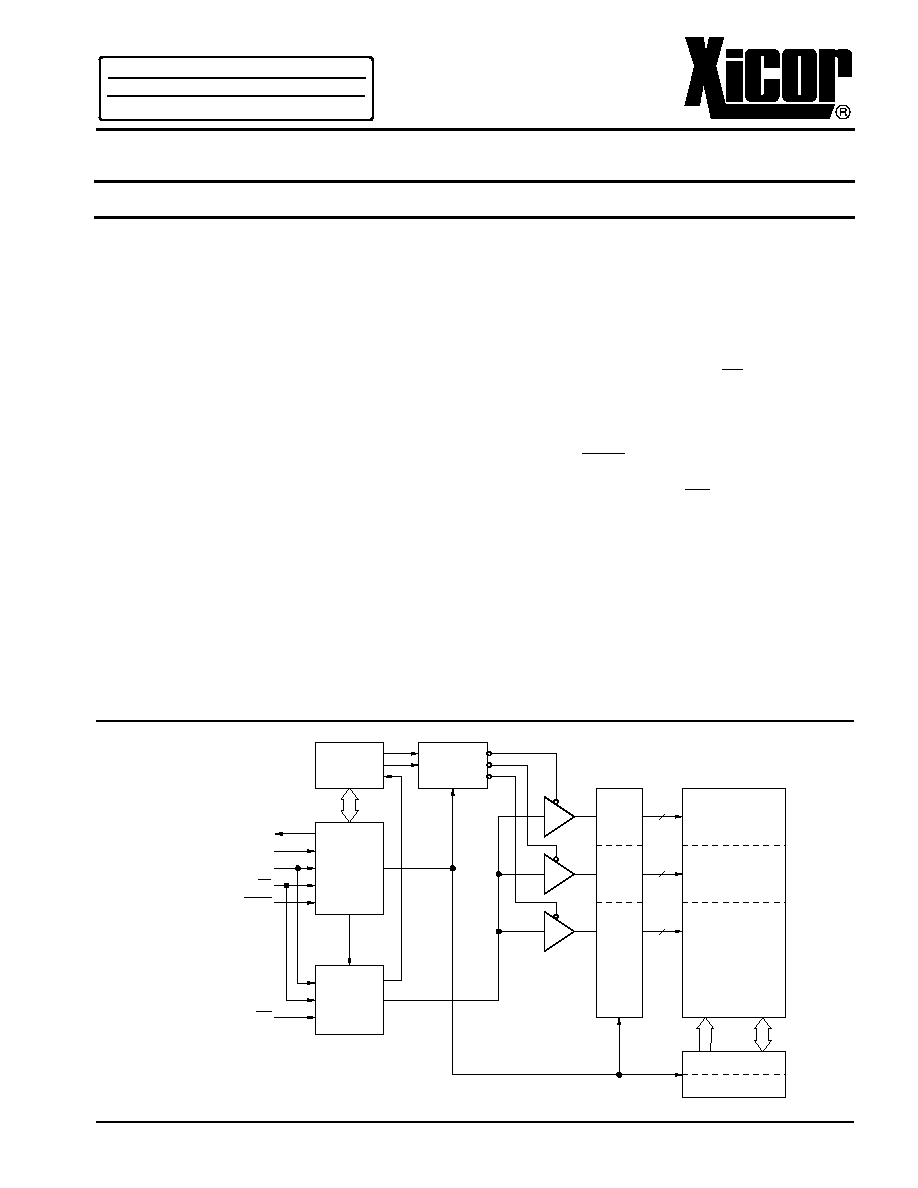
DESCRIPTION
The X25642 is a CMOS 65,536-bit serial E
2
PROM,
internally organized as 8K x 8. The X25642 features a
Serial Peripheral Interface (SPI) and software protocol
allowing operation on a simple three-wire bus. The bus
signals are a clock input (SCK) plus separate data in
(SI) and data out (SO) lines. Access to the device is
controlled through a chip select (CS) input, allowing
any number of devices to share the same bus.
The X25642 also features two additional inputs that
provide the end user with added flexibility. By
asserting the HOLD input, the X25642 will ignore tran-
sitions on its inputs, thus allowing the host to service
higher priority interrupts. The WP input can be used as
a hardwire input to the X25642 disabling all write
attempts to the status register, thus providing a mech-
anism for limiting end user capability of altering 0, 1/4,
1/2 or all of the memory.
The X25642 utilizes Xicor's proprietary Direct Write
TM
cell, providing a minimum endurance of 100,000
cycles and a minimum data retention of 100 years.
COMMAND
DECODE
AND
CONTROL
LOGIC
WRITE
CONTROL
AND
TIMING
LOGIC
WRITE
PROTECT
LOGIC
X DECODE
LOGIC
8K BYTE
ARRAY
64 X 256
Y DECODE
DATA REGISTER
SO
SI
SCK
CS
HOLD
WP
64
128
8
32
STATUS
REGISTER
64
128 X 256
64 X 256
3132 ILL F01.1
FUNCTIONAL DIAGRAM
Direct Write
TM
and Block Lock
TM
Protection is a trademark of Xicor, Inc.
A
PPLICATION
N
OTE
A V A I L A B L E
AN19 ∑ AN38 ∑ AN41 ∑ AN61
X25642
2
PIN DESCRIPTIONS
Serial Output (SO)
SO is a push/pull serial data output pin. During a read
cycle, data is shifted out on this pin. Data is clocked
out by the falling edge of the serial clock.
Serial Input (SI)
SI is the serial data input pin. All opcodes, byte
addresses, and data to be written to the memory are
input on this pin. Data is latched by the rising edge of
the serial clock.
Serial Clock (SCK)
The Serial Clock controls the serial bus timing for data
input and output. Opcodes, addresses, or data present
on the SI pin are latched on the rising edge of the
clock input, while data on the SO pin change after the
falling edge of the clock input.
Chip Select (CS)
When CS is HIGH, the X25642 is deselected and the
SO output pin is at high impedance and unless an
internal write operation is underway, the X25642 will be
in the standby power mode. CS LOW enables the
X25642, placing it in the active power mode. It should
be noted that after power-up, a HIGH to LOW transition
on CS is required prior to the start of any operation.
Write Protect (WP)
When WP is LOW and the nonvolatile bit WPEN is "1",
nonvolatile writes to the X25642 status register are
disabled, but the part otherwise functions normally.
When WP is held HIGH, all functions, including
nonvolatile writes operate normally. WP going LOW
while CS is still LOW will interrupt a write to the
X25642 status register. If the internal write cycle has
already been initiated, WP going LOW will have no
affect on a write.
The WP pin function is blocked when the WPEN bit in
the status register is "0". This allows the user to install
the X25642 in a system with WP pin grounded and still
be able to write to the status register. The WP pin func-
tions will be enabled when the WPEN bit is set "1".
Hold (HOLD)
HOLD is used in conjunction with the CS pin to select
the device. Once the part is selected and a serial
sequence is underway, HOLD may be used to pause
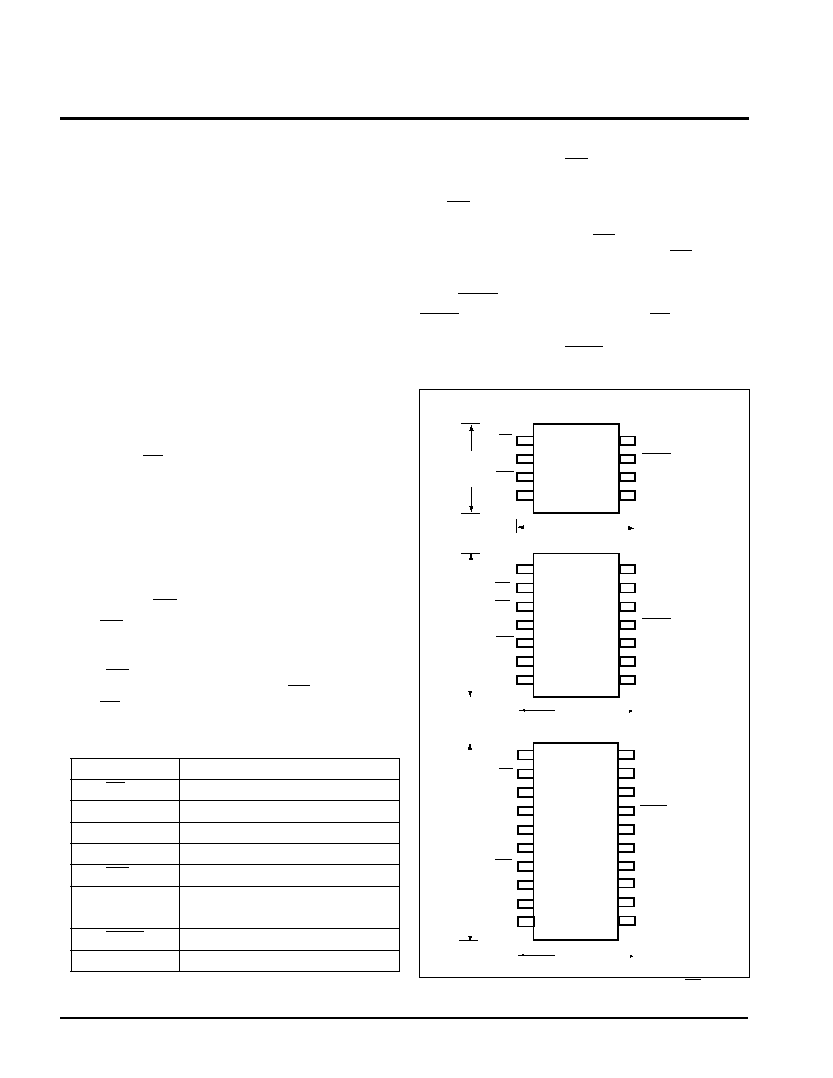
3132 ILL F02.5
CS
SO
WP
VSS
1
2
3
4
8
7
6
5
VCC
HOLD
SCK
SI
SOIC/DIP
NC
CS*
CS*
SO
WP
VSS
NC
1
2
3
4
5
6
7
14
13
12
11
10
9
8
NC
NC
VCC
HOLD
SCK
SI
NC
SOIC
X25642
X25642
NC
CS
NC
SO
NC
NC
WP
VSS
NC
NC
NC
VCC
NC
HOLD
NC
NC
SCK
SI
NC
NC
1
2
3
4
5
6
7
8
9
10
20
19
18
17
16
15
14
13
12
11
TSSOP
1
2
3
4
5
6
7
8
9
10
20
19
18
17
16
15
14
13
12
11
X25642
.300"
.345"
.197"
.244"
.244"
.252"
SOIC
Only
Not to Scale
* Pin 2 and Pin 3 are internally connected. Only one CS needs to
be connected externally.
PIN NAMES
7037 FRM T01
Symbol
Description
CS
Chip Select Input
SO
Serial Output
SI
Serial Input
SCK
Serial Clock Input
WP
Write Protect Input
V
SS
Ground
V
CC
Supply Voltage
HOLD
Hold Input
NC
No Connect
PIN CONFIGURATION
X25642
3
the serial communication with the controller without
resetting the serial sequence. To pause, HOLD must
be brought LOW while SCK is LOW. To resume
communication,
HOLD is brought HIGH, again while
SCK is LOW. If the pause feature is not used, HOLD
should be held HIGH at all times.
PRINCIPLES OF OPERATION
The X25642 is a 8K x 8 E
2
PROM designed to interface
directly with the synchronous serial peripheral inter-
face (SPI) of many popular microcontroller families.
The X25642 contains an 8-bit instruction register. It is
accessed via the SI input, with data being clocked in on
the rising SCK. CS must be LOW and the HOLD and
WP inputs must be HIGH during the entire operation.
Table 1 contains a list of the instructions and their
opcodes. All instructions, addresses and data are
transferred MSB first.
Data input is sampled on the first rising edge of SCK
after CS goes LOW. SCK is static, allowing the user to
stop the clock and then resume operations. If the clock
line is shared with other peripheral devices on the SPI
bus, the user can assert the
HOLD input to place the
X25642 into a "PAUSE" condition. After releasing
HOLD, the X25642 will resume operation from the
point when HOLD was first asserted.
Write Enable Latch
The X25642 contains a "write enable" latch. This latch
must be SET before a write operation will be
completed internally. The WREN instruction will set the
latch and the WRDI instruction will reset the latch. This
latch is automatically reset upon a power-up condition
and after the completion of a byte, page, or status
register write cycle.
Status Register
The RDSR instruction provides access to the status
register. The status register may be read at any time,
even during a write cycle. The status register is
formatted as follows:
7037 FRM T02
WPEN, BP0 and BP1 are set by the WRSR instruc-
tion. WEL and WIP are read-only and automatically set
by other operations.
The Write-In-Process (WIP) bit indicates whether the
X25642 is busy with a write operation. When set to a
"1", a write is in progress, when set to a "0", no write is
in progress. During a write, all other bits are set to "1".
The Write Enable Latch (WEL) bit indicates the status
of the "write enable" latch. When set to a "1", the latch
is set, when set to a "0", the latch is reset.
The Block Protect (BP0 and BP1) bits are nonvolatile
and allow the user to select one of four levels of
protection. The X25642 is divided into four 16384-bit
segments. One, two, or all four of the segments may
be protected. That is, the user may read the segments
but will be unable to alter (write) data within the
selected segments. The partitioning is controlled as
illustrated below.
7037 FRM T03
7
6
5
4
3
2
1
0
WPEN
X
X
X
BP1
BP0
WEL
WIP
Status Register Bits
Array Addresses
Protected
BP1
BP0
0
0
None
0
1
$1800≠$1FFF
1
0
$1000≠$1FFF
1
1
$0000≠$1FFF
Table 1. Instruction Set
7037 FRM T04
*Instructions are shown MSB in leftmost position. Instructions are transferred MSB first.
Instruction Name
Instruction Format*
Operation
WREN
0000 0110
Set the Write Enable Latch (Enable Write Operations)
WRDI
0000 0100
Reset the Write Enable Latch (Disable Write Operations)
RDSR
0000 0101
Read Status Register
WRSR
0000 0001
Write Status Register
READ
0000 0011
Read Data from Memory Array beginning at selected address
WRITE
0000 0010
Write Data to Memory Array beginning at Selected Address (1 to 32
Bytes)
X25642
4
Write-Protect Enable
The Write-Protect-Enable (WPEN) is available for the
X25642 as a nonvolatile enable bit for the WP pin.
7037 FRM T05
The Write Protect (WP) pin and the nonvolatile Write
Protect Enable (WPEN) bit in the Status Register
control the programmable hardware write protect
feature. Hardware write protection is enabled when WP
pin is LOW, and the WPEN bit is "1". Hardware write
protection is disabled when either the WP pin is HIGH
or the WPEN bit is "0". When the chip is hardware write
protected, nonvolatile writes are disabled to the Status
Register, including the Block Protect bits and the
WPEN bit itself, as well as the block-protected sections
in the memory array. Only the sections of the memory
array that are not block-protected can be written.
Note:
Since the WPEN bit is write protected, it cannot
be changed back to a "0", as long as the WP pin
is held LOW.
Clock and Data Timing
Data input on the SI line is latched on the rising edge
of SCK. Data is output on the SO line by the falling
edge of SCK.
Read Sequence
When reading from the E
2
PROM memory array, CS is
first pulled LOW to select the device. The 8-bit READ
instruction is transmitted to the X25642, followed by
the 16-bit address of which the last 13 are used. After
the READ opcode and address are sent, the data
stored in the memory at the selected address is
shifted out on the SO line. The data stored in memory
at the next address can be read sequentially by
continuing to provide clock pulses. The address is
automatically incremented to the next higher address
after each byte of data is shifted out. When the highest
address is reached ($1FFF) the address counter rolls
over to address $0000 allowing the read cycle to be
continued indefinitely. The read operation is termi-
nated by taking CS HIGH. Refer to the read E
2
PROM
array operation sequence illustrated in Figure 1.
WPEN
WP
WEL
Protected
Blocks
Unprotected
Blocks
Status
Register
0
X
0
Protected
Protected
Protected
0
X
1
Protected
Writable
Writable
1
LOW
0
Protected
Protected
Protected
1
LOW
1
Protected
Writable
Protected
X
HIGH
0
Protected
Protected
Protected
X
HIGH
1
Protected
Writable
Writable
To read the status register the
CS
line is first pulled
LOW to select the device followed by the 8-bit RDSR
instruction. After the RDSR opcode is sent, the contents
of the status register are shifted out on the SO line.
Figure 2 illustrates the read status register sequence.
Write Sequence
Prior to any attempt to write data into the X25642, the
"write enable" latch must first be set by issuing the
WREN instruction (See Figure 3). CS is first taken
LOW, then the WREN instruction is clocked into the
X25642. After all eight bits of the instruction are trans-
mitted, CS must then be taken HIGH. If the user
continues the write operation without taking CS HIGH
after issuing the WREN instruction, the write operation
will be ignored.
To write data to the E
2
PROM memory array, the user
issues the WRITE instruction, followed by the address
and then the data to be written. This is minimally a
thirty-two clock operation.
CS
must go LOW and
remain LOW for the duration of the operation. The host
may continue to write up to 32 bytes of data to the
X25642. The only restriction is the 32 bytes must reside
on the same page. If the address counter reaches the
end of the page and the clock continues, the counter
will "roll over" to the first address of the page and over-
write any data that may have been written.
For the write operation (byte or page write) to be
completed, CS can only be brought HIGH after bit 0 of
data byte N is clocked in. If it is brought HIGH at any
other time the write operation will not be completed.
Refer to Figures 4 and 5 below for a detailed illustra-
tion of the write sequences and time frames in which
CS going HIGH are valid.
To write to the status register, the WRSR instruction is
followed by the data to be written. Data bits 0, 1, 4, 5
and 6 must be "0". Figure 6 illustrates this sequence.
While the write is in progress following a status
register or E
2
PROM write sequence, the status
register may be read to check the WIP bit. During this
time the WIP bit will be HIGH.
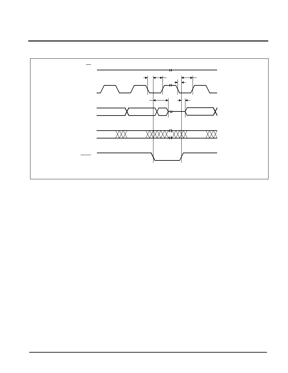
Hold Operation
The HOLD input should be HIGH (at V
IH
) under normal
operation. If a data transfer is to be interrupted HOLD
can be pulled LOW to suspend the transfer until it can
be resumed. The only restriction is the SCK input must
be LOW when HOLD is first pulled LOW and SCK
must also be LOW when HOLD is released.
The HOLD input may be tied HIGH either directly to
V
CC
or tied to V
CC
through a resistor.
X25642
5
Operational Notes
The X25642 powers-up in the following state:
∑ The device is in the low power standby state.
∑ A HIGH to LOW transition on CS is required to enter
an active state and receive an instruction.
∑ SO pin is high impedance.
∑ The "write enable" latch is reset.
Data Protection
The following circuitry has been included to prevent in-
advertent writes:
∑ The "write enable" latch is reset upon power-up.
∑ A WREN instruction must be issued to set the "write
enable" latch.
∑ CS must come HIGH at the proper clock count in or-
der to start a write cycle.
Figure 1. Read E
2
PROM Array Operation Sequence
0
1
2
3
4
5
6
7
8
9
10
20 21 22 23 24 25 26 27 28 29 30
7
6
5
4
3
2
1
0
DATA OUT
CS
SCK
SI
SO
MSB
HIGH IMPEDANCE
INSTRUCTION
16 BIT ADDRESS
15 14 13
3
2
1
0
3132 ILL F03.1
Figure 2. Read Status Register Operation Sequence
0
1
2
3
4
5
6
7
8
9
10
11
12 13 14
7
6
5
4
3
2
1
0
DATA OUT
CS
SCK
SI
SO
MSB
HIGH IMPEDANCE
INSTRUCTION
3132 ILL F04
X25642
6
Figure 3. Write Enable Latch Sequence
Figure 4. Byte Write Operation Sequence
0
1
2
3
4
5
6
7
3132 ILL F05
CS
SI
SCK
HIGH IMPEDANCE
SO
0
1
2
3
4
5
6
7
8
9
10
CS
SCK
SI
SO
HIGH IMPEDANCE
INSTRUCTION
16 BIT ADDRESS
DATA BYTE
7
6
5
4
3
2
1
0
15 14 13
3
2
1
0
20 21 22 23 24 25 26 27 28 29 30 31
3132 ILL F06.1
X25642
7
Figure 6. Write Status Register Operation Sequence
Figure 5. Page Write Operation Sequence
32 33 34 35 36 37 38 39
SCK
SI
CS
0
1
2
3
4
5
6
7
8
9
10
SCK
SI
INSTRUCTION
16 BIT ADDRESS
DATA BYTE 1
7
6
5
4
3
2
1
0
CS
40 41 42 43 44 45 46 47
DATA BYTE 2
7
6
5
4
3
2
1
0
DATA BYTE 3
7
6
5
4
3
2
1
0
DATA BYTE N
15 14 13
3
2
1
0
20 21 22 23 24 25 26 27 28 29 30 31
6
5
4
3
2
1
0
3132 ILL F07
0
1
2
3
4
5
6
7
8
9
CS
SCK
SI
SO
HIGH IMPEDANCE
INSTRUCTION
DATA BYTE
7
6
5
4
3
2
1
0
10 11 12 13 14 15
3132 ILL F08.1
X25642
8
ABSOLUTE MAXIMUM RATINGS*
Temperature under Bias....................≠65
∞
C to +135
∞
C
Storage Temperature ........................≠65
∞
C to +150
∞
C
Voltage on any Pin with Respect
to V
SS
.........................................................≠1V to +7V
D.C. Output Current ............................................. 5mA
(Soldering, 10 seconds) ..............................300
∞
C
D.C. OPERATING CHARACTERISTICS
(Over the recommended operating conditions unless otherwise specified.)
7037 FRM T08
POWER-UP TIMING
7037 FRM T09
CAPACITANCE
T
A
= +25
∞
C, f = 1MHz, V
CC
= 5V
7037 FRM T10
Notes:
(1) V
IL
min. and V
IH
max. are for reference only and are not tested.
(2) This parameter is periodically sampled and not 100% tested.
(3) t
PUR
and t
PUW
are the delays required from the time V
CC
is stable until the specified operation can be initiated. These
parameters are periodically sampled and not 100% tested.
Symbol
Parameter
Limits
Units
Test Conditions
Min.
Max.
I
CC
V
CC
Supply Current (Active)
5
mA
SCK = V
CC
x 0.1/V
CC
x 0.9 @ 2MHz,
I
SB
V
CC
Supply Current (Standby)
1
µ
A
CS
= V
CC
, V
IN
=
V
SS
or V
CC
≠ 0.3V
I
LI
Input Leakage Current
10
µ
A
V
IN
=
V
SS
to V
CC
I
LO
Output Leakage Current
10
µ
A
V
OUT
=
V
SS
to V
CC
V
IL
(1)
Input LOW Voltage
≠1
V
CC
x 0.3
V
V
IH
(1)
Input HIGH Voltage
V
CC
x 0.7
V
CC
+ 0.5
V
V
OL1
Output LOW Voltage
0.4
V
I
OL
= 3mA, V
CC
= 5V
V
OH1
Output HIGH Voltage
V
CC
≠0.8
V
I
OH
= ≠1.6mA, V
CC
= 5V
V
OL2
Output LOW Voltage
0.4
V
I
OL
= 1.5mA, V
CC
= 3V
V
OH2
Output HIGH Voltage
V
CC
≠0.3
V
I
OH
= ≠0.4mA, V
CC
= 3V
Symbol
Parameter
Min.
Max.
Units
T
PUR
(3)
Power-up to Read Operation
1
ms
T
PUW
(3)
Power-up to Write Operation
1
ms
Symbol
Parameter
Max.
Units
Test Conditions
C
I/O
(3)
Output Capacitance (SO)
8
pF
V
I/O
= 0V
C
IN
(3)
Input Capacitance (SCK, SI,
CS
,
WP
,
HOLD
)
6
pF
V
IN
= 0V
RECOMMENDED OPERATING CONDITIONS
7037 FRM T06
Temperature
Min.
Max.
Commercial
0
∞
C
+70
∞
C
Industrial
≠40
∞
C
+85
∞
C
Military
≠55
∞
C
+125
∞
C
7037 FRM T07
Supply Voltage
Limits
X25642
5V
±
10%
X25642-2.7
2.7V to 5.5V
*COMMENT
Stresses above those listed under "Absolute Maximum
Ratings" may cause permanent damage to the device.
This is a stress rating only and the functional operation
of the device at these or any other conditions above
those indicated in the operational sections of this
specification is not implied. Exposure to absolute
maximum rating conditions for extended periods may
affect device reliability.
X25642
9
A.C. OPERATING CHARACTERISTICS
Data Input Timing
7037 FRM T12
Data Output Timing
7037 FRM T13
Notes: (4) This parameter is periodically sampled and not 100% tested.
(5) t
WC
is the time from the rising edge of CS after a valid write sequence has been sent to the end of the self-timed internal nonvolatile
write cycle.
Symbol Parameter Min.
Max.
Units
f
SCK
Clock Frequency
0
2
MHz
t
CYC
Cycle Time
500
ns
t
LEAD
CS Lead Time
250
ns
t
LAG
CS Lag Time
250
ns
t
WH
Clock HIGH Time
200
ns
t
WL
Clock LOW Time
200
ns
t
SU
Data Setup Time
50
ns
t
H
Data Hold Time
50
ns
t
RI
(4)
Data In Rise Time
2
µ
s
t
FI
(4)
Data In Fall Time
2
µ
s
t
HD
HOLD
Setup Time
100
ns
t
CD
HOLD
Hold Time
100
ns
t
CS
CS
Deselect Time
2.0
µ
s
t
WC
(5)
Write Cycle Time
10
ms
Symbol Parameter
Min.
Max.
Units
f
SCK
Clock Frequency
0
2
MHz
t
DIS
Output Disable Time
250
ns
t
V
Output Valid from Clock LOW
200
ns
t
HO
Output Hold Time
0
ns
t
RO
(4)
Output Rise Time
100
ns
t
FO
(4)
Output Fall Time
100
ns
t
LZ
(4)
HOLD
HIGH to Output in Low Z
100
ns
t
HZ
(4)
HOLD
LOW to Output in High Z
100
ns
A.C. CONDITIONS OF TEST
7037 FRM T11
Input Pulse Levels
V
CC
x 0.1 to V
CC
x 0.9
Input Rise and Fall Times
10ns
Input and OutputTiming Levels
V
CC
X 0.5
EQUIVALENT A.C. LOAD CIRCUIT
OUTPUT
3132 ILL F09.2
5V
1.44K
1.95K
100pF
OUTPUT
3V
1.64K
4.63K
100pF
X25642
10
Serial Output Timing
SCK
CS
SO
SI
MSB OUT
MSB≠1 OUT
LSB OUT
ADDR
LSB IN
t
CYC
t
V
t
HO
t
WL
t
WH
t
DIS
3132 ILL F10.1
t
LAG
Serial Input Timing
SCK
CS
SI
SO
MSB IN
t
SU
t
RI
t
LAG
3132 ILL F11
t
LEAD
t
H
LSB IN
t
CS
t
FI
HIGH IMPEDANCE
X25642
11
Hold Timing
SCK
CS
SI
SO
t
HD
3132 ILL F12.1
t
LZ
HOLD
t
CD
t
HZ
t
CD
t
HD
X25642
12
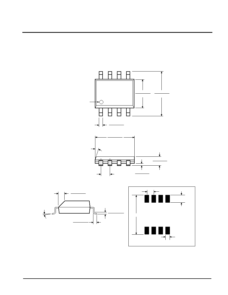
PACKAGING INFORMATION
3926 FHD F01
NOTE:
1. ALL DIMENSIONS IN INCHES (IN PARENTHESES IN MILLIMETERS)
2. PACKAGE DIMENSIONS EXCLUDE MOLDING FLASH
0.020 (0.51)
0.016 (0.41)
0.150 (3.81)
0.125 (3.18)
0.110 (2.79)
0.090 (2.29)
0.430 (10.92)
0.360 (9.14)
0.300
(7.62) REF.
PIN 1 INDEX
0.145 (3.68)
0.128 (3.25)
0.025 (0.64)
0.015 (0.38)
PIN 1
SEATING
PLANE
0.065 (1.65)
0.045 (1.14)
0.260 (6.60)
0.240 (6.10)
0.060 (1.52)
0.020 (0.51)
TYP. 0.010 (0.25)
0
∞
15
∞
8-LEAD PLASTIC DUAL IN-LINE PACKAGE TYPE P
HALF SHOULDER WIDTH ON
ALL END PINS OPTIONAL
0.015 (0.38)
MAX.
0.325 (8.25)
0.300 (7.62)
X25642
13
PACKAGING INFORMATION
0.150 (3.80)
0.158 (4.00)
0.228 (5.80)
0.244 (6.20)
0.014 (0.35)
0.019 (0.49)
PIN 1
PIN 1 INDEX
0.010 (0.25)
0.020 (0.50)
0.050 (1.27)
0.188 (4.78)
0.197 (5.00)
0.004 (0.19)
0.010 (0.25)
0.053 (1.35)
0.069 (1.75)
(4X) 7
∞
0.016 (0.410)
0.037 (0.937)
0.0075 (0.19)
0.010 (0.25)
0
∞
≠ 8
∞
X 45
∞
3926 FHD F22.1
8-LEAD PLASTIC SMALL OUTLINE GULL WING PACKAGE TYPE S
NOTE: ALL DIMENSIONS IN INCHES (IN PARENTHESES IN MILLIMETERS)
0.250"
0.050" TYPICAL
0.050"
TYPICAL
0.030"
TYPICAL
8 PLACES
FOOTPRINT
X25642
14
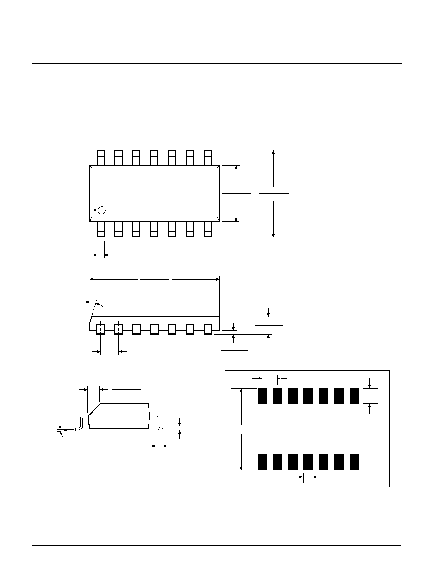
PACKAGING INFORMATION
0.150 (3.80)
0.158 (4.00)
0.228 (5.80)
0.244 (6.20)
0.014 (0.35)
0.020 (0.51)
PIN 1
PIN 1 INDEX
0.010 (0.25)
0.020 (0.50)
0.050 (1.27)
0.336 (8.55)
0.345 (8.75)
0.004 (0.10)
0.010 (0.25)
0.053 (1.35)
0.069 (1.75)
(4X) 7
∞
0.016 (0.41)
0.037 (0.937)
0.0075 (0.19)
0.010 (0.25)
0
∞
≠ 8
∞
X 45
∞
3926 FHD F10
14-LEAD PLASTIC SMALL OUTLINE GULL WING PACKAGE TYPE S
NOTE: ALL DIMENSIONS IN INCHES (IN PARENTHESES IN MILLIMETERS)
0.250"
0.050" Typical
0.050" Typical
0.030" Typical
14 Places
FOOTPRINT
X25642
15
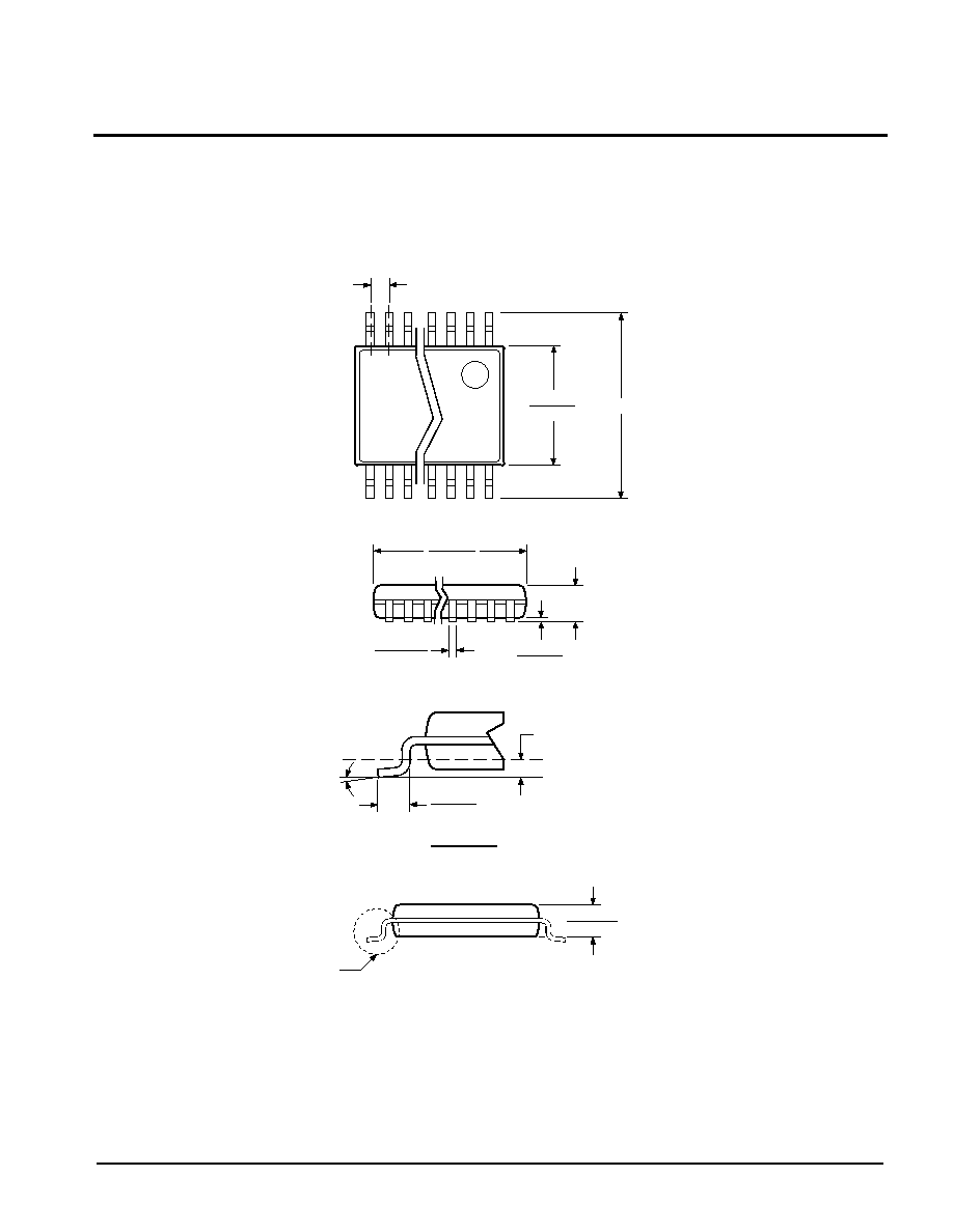
NOTE: ALL DIMENSIONS IN INCHES (IN PARENTHESES IN MILLIMETERS)
20-LEAD PLASTIC, TSSOP PACKAGE TYPE V
See Detail "A"
.031 (.80)
.041 (1.05)
.169 (4.3)
.177 (4.5)
.252 (6.4) BSC
.025 (.65) BSC
.252 (6.4)
.300 (6.6)
.002 (.05)
.006 (.15)
.047 (1.20)
.0075 (.19)
.0118 (.30)
0
∞
≠ 8
∞
.010 (.25)
.019 (.50)
.029 (.75)
Gage Plane
Seating Plane
Detail A (20X)
3926 FHD F45
PACKAGING INFORMATION
X25642
16
ORDERING INFORMATION
Part Mark Convention
X25642
P
-V
Device
V
CC
Limits
Blank = 5V
±
10%
2.7 = 2.7 to 5.5V
Temperature Range
Blank = Commercial = 0
∞
C to +70
∞
C
I = Industrial = ≠40
∞
C to +85
∞
C
M = Military = ≠55
∞
C to +125
∞
C
Package
P = 8-Lead Plastic DIP
LIMITED WARRANTY
Devices sold by Xicor, Inc. are covered by the warranty and patent indemnification provisions appearing in its Terms of Sale only. Xicor, Inc.
makes no warranty, express, statutory, implied, or by description regarding the information set forth herein or regarding the freedom of the
described devices from patent infringement. Xicor, Inc. makes no warranty of merchantability or fitness for any purpose. Xicor, Inc. reserves the
right to discontinue production and change specifications and prices at any time and without notice.
Xicor, Inc. assumes no responsibility for the use of any circuitry other than circuitry embodied in a Xicor, Inc. product. No other circuits, patents,
licenses are implied.
U.S. PATENTS
Xicor products are covered by one or more of the following U.S. Patents: 4,263,664; 4,274,012; 4,300,212; 4,314,265; 4,326,134; 4,393,481;
4,404,475; 4,450,402; 4,486,769; 4,488,060; 4,520,461; 4,533,846; 4,599,706; 4,617,652; 4,668,932; 4,752,912; 4,829, 482; 4,874, 967;
4,883, 976. Foreign patents and additional patents pending.
LIFE RELATED POLICY
In situations where semiconductor component failure may endanger life, system designers using this product should design the system with
appropriate error detection and correction, redundancy and back-up features to prevent such an occurence.
Xicor's products are not authorized for use in critical components in life support devices or systems.
1. Life support devices or systems are devices or systems which, (a) are intended for surgical implant into the body, or (b) support or sustain
life, and whose failure to perform, when properly used in accordance with instructions for use provided in the labeling, can be reasonably
expected to result in a significant injury to the user.
2. A critical component is any component of a life support device or system whose failure to perform can be reasonably expected to cause the
failure of the life support device or system, or to affect its safety or effectiveness.
X25642
X
X
P = 8-Lead Plastic DIP
S = 14-Lead SOIC
Blank = 5V
±
10%, 0
∞
C to +70
∞
C
I = 5V
±
10%, ≠40
∞
C to +85
∞
C
M = 5V
±
10%, ≠55
∞
C to +125
∞
C
F = 2.7V to 5.5V, 0
∞
C to 70
∞
C
G = 2.7V to 5.5V, ≠40
∞
C to +85
∞
C
S = 14-Lead SOIC
Blank = 8 Lead SOIC
T
V = 20-Lead TSSOP
V = 20-Lead TSSOP
S8 = 8-Lead SOIC