Document Outline
- Table of Contents
- Product Selection
- Data Sheet Alpha
- Ap Note Alpha
X28C256
1
5 Volt, Byte Alterable E
2
PROM
© Xicor, Inc. 1991, 1995 Patents Pending
Characteristics subject to change without notice
3855-1.9 8/1/97 T1/C0/D8 EW
DESCRIPTION
The X28C256 is an 32K x 8 E
2
PROM, fabricated with
Xicor's proprietary, high performance, floating gate
CMOS technology. Like all Xicor programmable non-
volatile memories the X28C256 is a 5V only device. The
X28C256 features the JEDEC approved pinout for byte-
wide memories, compatible with industry standard RAMs.
The X28C256 supports a 64-byte page write operation,
effectively providing a 78
µ
s/byte write cycle and en-
abling the entire memory to be typically written in less
than 2.5 seconds. The X28C256 also features
DATA
and Toggle Bit Polling, a system software support
scheme used to indicate the early completion of a write
cycle. In addition, the X28C256 includes a user-optional
software data protection mode that further enhances
Xicor's hardware write protect capability.
Xicor E
2
PROMs are designed and tested for applica-
tions requiring extended endurance. Inherent data re-
tention is greater than 100 years.
FEATURES
∑
Access Time: 200ns
∑
Simple Byte and Page Write
-- Single 5V Supply
--No External High Voltages or V
PP
Control
Circuits
-- Self-Timed
--No Erase Before Write
--No Complex Programming Algorithms
--No Overerase Problem
∑
Low Power CMOS:
--Active: 60mA
--Standby: 200
µ
A
∑
Software Data Protection
-- Protects Data Against System Level
Inadvertent Writes
∑
High Speed Page Write Capability
∑
Highly Reliable Direct Write
TM
Cell
-- Endurance: 100,000 Write Cycles
-- Data Retention: 100 Years
∑
Early End of Write Detection
--
DATA
Polling
--Toggle Bit Polling
256K
X28C256
32K x 8 Bit
PIN CONFIGURATION
A14
A12
A7
A6
A5
A4
A3
A2
A1
A0
I/O0
I/O1
I/O2
VSS
1
2
3
4
5
6
7
8
9
10
11
12
13
14
28
27
26
25
24
23
22
21
20
19
18
17
16
15
VCC
WE
A13
A8
A9
A11
OE
A10
CE
I/O7
I/O6
I/O5
I/04
I/O3
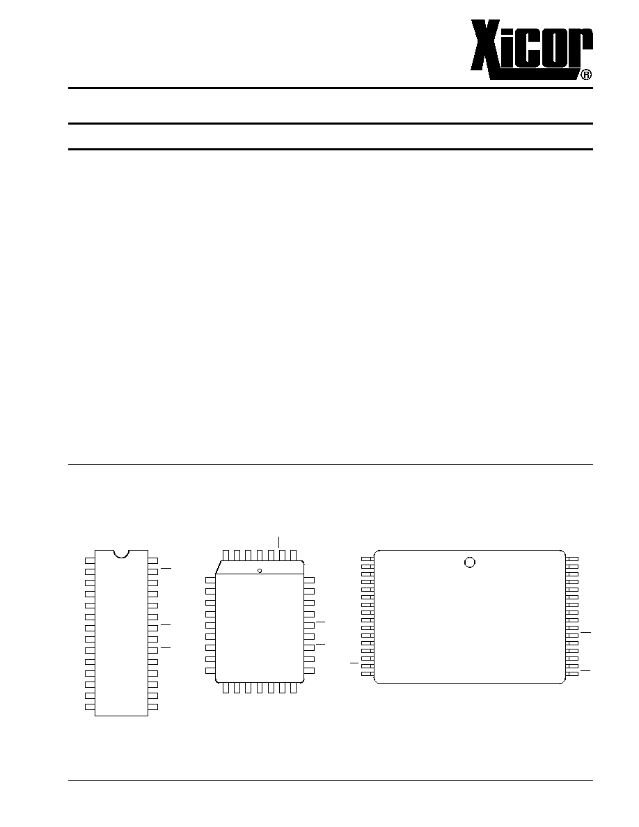
X28C256
PLASTIC DIP
CERDIP
FLAT PACK
SOIC
3855 FHD F02
TSOP
1
2
3
4
5
6
7
8
9
10
11
12
13
14
15
16
X28C256
A3
A4
A5
A6
A7
A12
A14
NC
VCC
NC
WE
A13
A8
A9
A11
OE
32
31
30
29
28
27
26
25
24
23
22
21
20
19
18
17
A2
A1
A0
I/O0
I/O1
I/O2
NC
VSS
NC
I/O3
I/O4
I/O5
I/O6
I/O7
CE
A10
3855 ILL F23
A6
A5
A4
A3
A2
A1
A0
NC
I/O0
A8
A9
A11
NC
OE
A10
CE
I/O7
I/O6
4
3
2
1 32 31 30
14 15 16 17 18 19 20
5
6
7
8
9
10
11
12
13
29
28
27
26
25
24
23
22
21
X28C256
A
7
A
12
A
14
NC
V
CC
WE
A
13
I/O
1
I/O
2
V
SS
NC
I/O
3
I/O
4
I/O
5
LCC
PLCC
3855 FHD F03
2
X28C256
PIN DESCRIPTIONS
Addresses (A
0
≠A
14
)
The Address inputs select an 8-bit memory location
during a read or write operation.
Chip Enable (
CE
)
The Chip Enable input must be LOW to enable all read/
write operations. When
CE
is HIGH, power consumption
is reduced.
Output Enable (
OE
)
The Output Enable input controls the data output buffers
and is used to initiate read operations.
Data In/Data Out (I/O
0
≠I/O
7
)
Data is written to or read from the X28C256 through the
I/O pins.
Write Enable (
WE
)
The Write Enable input controls the writing of data to the
X28C256.
PIN NAMES
Symbol
Description
A
0
≠A
14
Address Inputs
I/O
0
≠I/O
7
Data Input/Output
WE
Write Enable
CE
Chip Enable
OE
Output Enable
V
CC
+5V
V
SS
Ground
NC
No Connect
3855 PGM T01
3855 FHD F01
X BUFFERS
LATCHES AND
DECODER
I/O BUFFERS
AND LATCHES
Y BUFFERS
LATCHES AND
DECODER
CONTROL
LOGIC AND
TIMING
256K-BIT
E2PROM
ARRAY
I/O0≠I/O7
DATA INPUTS/OUTPUTS
CE
OE
VCC
VSS
A0≠A14
ADDRESS
INPUTS
WE
FUNCTIONAL DIAGRAM
X28C256
11
I/O0
10
A0
14
VSS
9
A1
8
A2
7
A3
6
A4
5
A5
2
A12
28
VCC
12
I/O1
13
I/O2
15
I/O3
4
A6
3
A7
1
A14
16
I/O4
20
CE
22
OE
24
A9
17
I/O5
27
WE
19
I/O7
21
A10
23
A11
25
A8
18
I/O6
26
A13
BOTTOM VIEW
PGA
3855 FHD F04
PIN CONFIGURATION
X28C256
3
DEVICE OPERATION
Read
Read operations are initiated by both
OE
and
CE
LOW.
The read operation is terminated by either
CE
or
OE
returning HIGH. This two line control architecture elimi-
nates bus contention in a system environment. The data
bus will be in a high impedance state when either
OE
or
CE
is HIGH.
Write
Write operations are initiated when both
CE
and
WE
are
LOW and
OE
is HIGH. The X28C256 supports both a
CE
and
WE
controlled write cycle. That is, the address is
latched by the falling edge of either
CE
or
WE
, whichever
occurs last. Similarly, the data is latched internally by the
rising edge of either
CE
or
WE
, whichever occurs first.
A byte write operation, once initiated, will automatically
continue to completion, typically within 5ms.
Page Write Operation
The page write feature of the X28C256 allows the entire
memory to be written in 2.5 seconds. Page write allows
two to sixty-four bytes of data to be consecutively written
to the X28C256 prior to the commencement of the
internal programming cycle. The host can fetch data
from another device within the system during a page
write operation (change the source address), but the
page address (A
6
through A
14
) for each subsequent
valid write cycle to the part during this operation must be
the same as the initial page address.
The page write mode can be initiated during any write
operation. Following the initial byte write cycle, the host
can write an additional one to sixty-three bytes in the
same manner as the first byte was written. Each succes-
sive byte load cycle, started by the
WE
HIGH to LOW
transition, must begin within 100
µ
s of the falling edge of
the preceding
WE
. If a subsequent
WE
HIGH to LOW
transition is not detected within 100
µ
s, the internal
automatic programming cycle will commence. There is
no page write window limitation. Effectively the page
write window is infinitely wide, so long as the host
continues to access the device within the byte load cycle
time of 100
µ
s.
DATA
Polling (I/O
7
)
The X28C256 features
DATA
Polling as a method to
indicate to the host system that the byte write or page
write cycle has completed.
DATA
Polling allows a simple
bit test operation to determine the status of the X28C256,
eliminating additional interrupt inputs or external hard-
ware. During the internal programming cycle, any at-
tempt to read the last byte written will produce the
complement of that data on I/O
7
(i.e. write data = 0xxx
xxxx, read data = 1xxx xxxx). Once the programming
cycle is complete, I/O
7
will reflect true data. Note: If the
X28C256 is in the protected state and an illegal write
operation is attempted
DATA
Polling will not operate.
Toggle Bit (I/O
6
)
The X28C256 also provides another method for deter-
mining when the internal write cycle is complete. During
the internal programming cycle I/O
6
will toggle from
HIGH to LOW and LOW to HIGH on subsequent
attempts to read the device. When the internal cycle is
complete the toggling will cease and the device will be
accessible for additional read or write operations.
Write Operation Status Bits
The X28C256 provides the user two write operation
status bits. These can be used to optimize a system
write cycle time. The status bits are mapped onto the
I/O bus as shown in Figure 1.
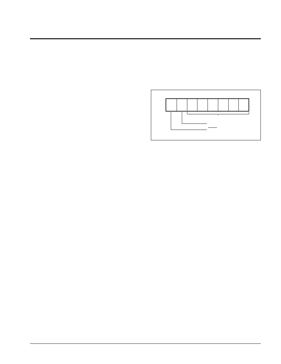
Figure 1. Status Bit Assignment
5
TB
DP
4
3
2
1
0
I/O
RESERVED
TOGGLE BIT
DATA POLLING
3855 FHD F11
4
X28C256
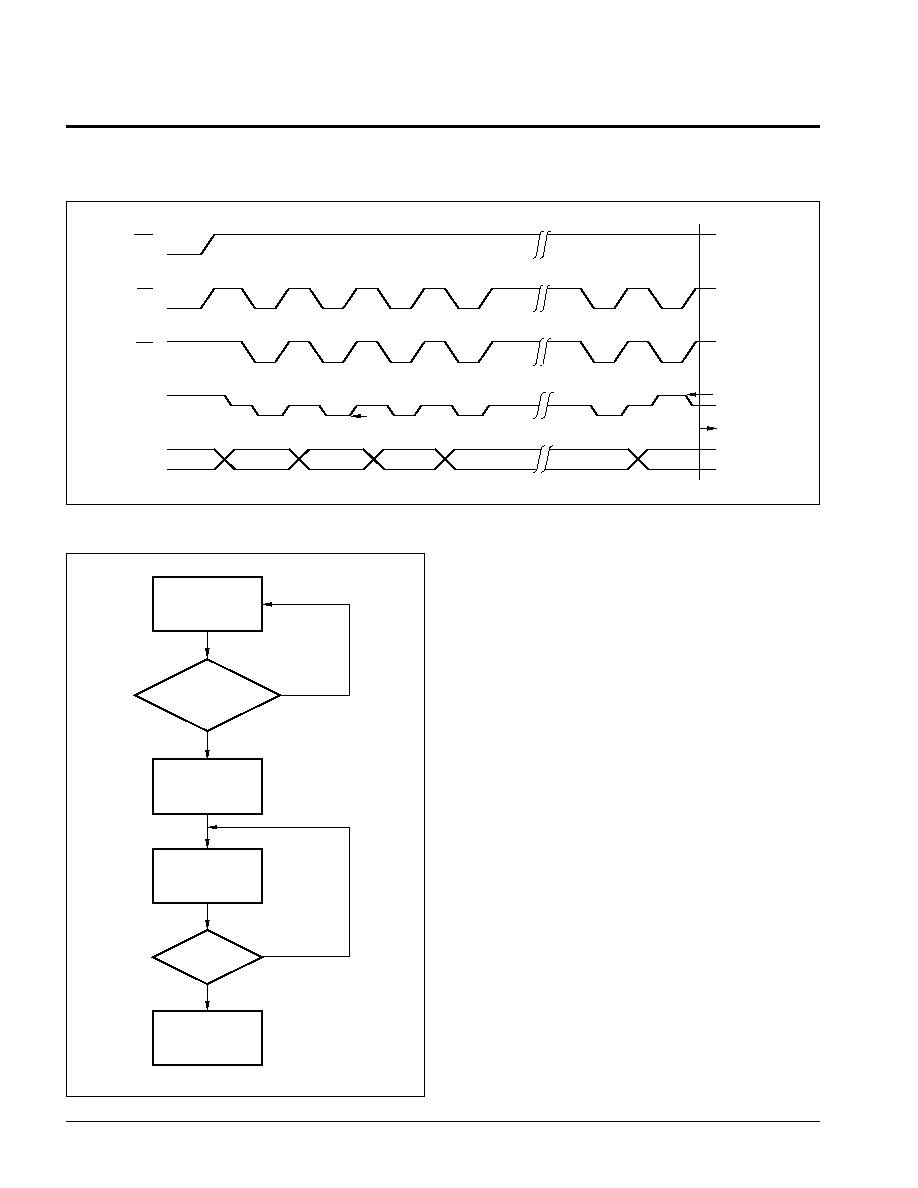
DATA
POLLING I/O
7
Figure 2.
DATA
Polling Bus Sequence
Figure 3.
DATA
Polling Software Flow
3855 FHD F13
DATA
Polling can effectively halve the time for writing to
the X28C256. The timing diagram in Figure 2 illustrates
the sequence of events on the bus. The software flow
diagram in Figure 3 illustrates one method of implement-
ing the routine.
3855 FHD F12
CE
OE
WE
I/O7
X28C256
READY
LAST
WRITE
HIGH Z
VOL
VIH
A0≠A14
An
An
An
An
An
An
VOH
An
WRITE DATA
SAVE LAST DATA
AND ADDRESS
READ LAST
ADDRESS
IO7
COMPARE?
X28C256
READY
NO
YES
WRITES
COMPLETE?
NO
YES
X28C256
5
THE TOGGLE BIT I/O
6
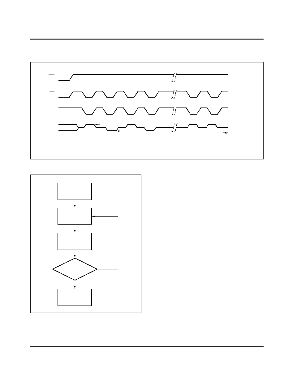
Figure 4. Toggle Bit Bus Sequence
CE
OE
WE
I/O6
X28C256
READY
VOH
VOL
LAST
WRITE
HIGH Z
* Beginning and ending state of I/O6 will vary.
*
*
3855 FHD F14
Figure 5. Toggle Bit Software Flow
3855 FHD F15
The Toggle Bit can eliminate the software housekeeping
chore of saving and fetching the last address and data
written to a device in order to implement
DATA
Polling.
This can be especially helpful in an array comprised of
multiple X28C256 memories that is frequently updated.
The timing diagram in Figure 4 illustrates the sequence
of events on the bus. The software flow diagram in
Figure 5 illustrates a method for polling the Toggle Bit.
LOAD ACCUM
FROM ADDR n
COMPARE
ACCUM WITH
ADDR n
X28C256
READY
COMPARE
OK?
NO
YES
LAST WRITE