Document Outline
- Table of Contents
- Product Selection
- Data Sheet Alpha
- Ap Note Alpha
X28HT512
1
512K
X28HT512
64K x 8 Bit
High Temperature, 5 Volt, Byte Alterable E
2
PROM
© Xicor, Inc. 1991, 1995, 1996 Patents Pending
Characteristics subject to change without notice
6614-1.5 8/5/97 T2/C0/D0 EW
FEATURES
∑
175
∞
C Full Functionality
∑
Simple Byte and Page Write
--Single 5V Supply
--Self-Timed
--No Erase Before Write
--No Complex Programming Algorithms
--No Overerase Problem
∑
Highly Reliable Direct WriteTM Cell
--Endurance: 10,000 Write Cycles
--Data Retention: 100 Years
--Higher Temperature Functionality is Possible
by Operating in the Byte Mode
DESCRIPTION
The X28HT512 is an 64K x 8 CMOS E
2
PROM, fabri-
cated with Xicor's proprietary, high performance, float-
ing gate CMOS technology which provides Xicor prod-
ucts superior high temperature performance character-
istics. Like all Xicor programmable nonvolatile memo-
ries the X28HT512 is a 5V only device. The X28HT512
features the JEDEC approved pinout for bytewide memo-
ries, compatible with industry standard EPROMS.
The X28HT512 supports a 128-byte page write opera-
tion, effectively providing a 39
µ
s/byte write cycle and
enabling the entire memory to be written in less than 2.5
seconds.
6614 FHD F02.1
VBB
NC
A15
A12
A7
A6
A5
A4
A3
A2
A1
A0
I/O0
I/O1
I/O2
VSS
1
2
3
4
5
6
7
8
9
10
11
12
13
14
15
16
32
31
30
29
28
27
26
25
24
23
22
21
20
19
18
17
VCC
WE
NC
A14
A13
A8
A9
A11
OE
A10
CE
I/O7
I/O6
I/O5
I/04
I/O3
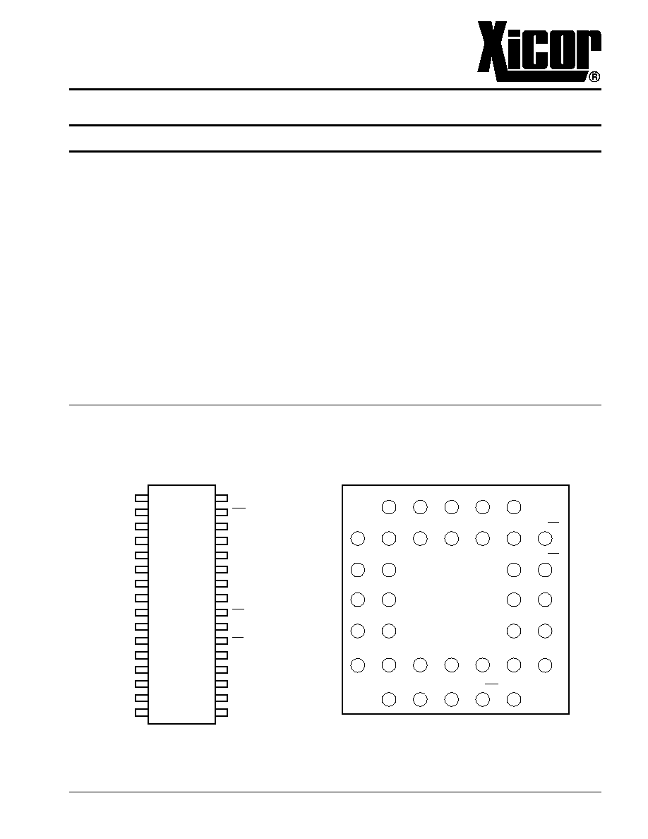
X28HT512
FLAT PACK
CERDIP
SOIC (R)
PIN CONFIGURATION
X28HT512
(BOTTOM VIEW)
14
A0
16
I/O1
18
VSS
11
A3
9
A5
7
A7
15
I/O0
17
I/O2
19
I/O3
5
A15
2
NC
36
VCC
20
I/O4
21
I/O5
34
NC
23
I/O7
25
A10
27
A11
29
A8
22
I/O6
32
NC
6614 FHD F23
24
CE
26
OE
28
A9
30
A13
13
A1
12
A2
10
A4
8
A6
4
3
V
BB
1
NC
35
WE
33
NC
31
A14
6
A12
PGA
NC

2
X28HT512
PIN DESCRIPTIONS
Addresses (A
0
≠A
15
)
The Address inputs select an 8-bit memory location
during a read or write operation.
Chip Enable (
CE
)
The Chip Enable input must be LOW to enable all read/
write operations. When
CE
is HIGH, power consumption
is reduced.
Output Enable (
OE
)
The Output Enable input controls the data output buffers
and is used to initiate read operations.
Data In/Data Out (I/O
0
≠I/O
7
)
Data is written to or read from the X28HT512 through the
I/O pins.
Back Bias Voltage (V
BB
)
It is required to provide -3V on pin 1. This negative
voltage improves higher temperature functionality.
PIN NAMES
Symbol
Description
A
0
≠A
15
Address Inputs
I/O
0
≠I/O
7
Data Input/Output
WE
Write Enable
CE
Chip Enable
OE
Output Enable
V
BB
≠3V
V
CC
+5V
V
SS
Ground
NC
No Connect
6614 PGM T01
Write Enable (
WE
)
The Write Enable input controls the writing of data to the
X28HT512.
FUNCTIONAL DIAGRAM
X BUFFERS
LATCHES AND
DECODER
I/O BUFFERS
AND LATCHES
6614 FHD F01
Y BUFFERS
LATCHES AND
DECODER
CONTROL
LOGIC AND
TIMING
512K-BIT
E2PROM
ARRAY
I/O0≠I/O7
DATA INPUTS/OUTPUTS
CE
OE
VCC
VSS
A7≠A15
WE
A0≠A6
VBB

X28HT512
3
DEVICE OPERATION
Read
Read operations are initiated by both
OE
and
CE
LOW.
The read operation is terminated by either
CE
or
OE
returning HIGH. This two line control architecture elimi-
nates bus contention in a system environment. The data
bus will be in a high impedance state when either
OE
or
CE
is HIGH.
Write
Write operations are initiated when both
CE
and
WE
are
LOW and
OE
is HIGH. The X28HT512 supports both a
CE
and
WE
controlled write cycle. That is, the address
is latched by the falling edge of either
CE
or
WE
,
whichever occurs last. Similarly, the data is latched
internally by the rising edge of either
CE
or
WE
, which-
ever occurs first. A byte write operation, once initiated,
will automatically continue to completion, typically within
5ms.
Page Write Operation
The page write feature of the X28HT512 allows the
entire memory to be written in 2.5 seconds. Page write
allows two to one hundred twenty-eight bytes of data to
be consecutively written to the X28HT512 prior to the
commencement of the internal programming cycle. The
host can fetch data from another device within the
system during a page write operation (change the source
address), but the page address (A
7
through A
15
) for
each subsequent valid write cycle to the part during this
operation must be the same as the initial page address.
The page write mode can be initiated during any write
operation. Following the initial byte write cycle, the host
can write an additional one to one hundred twenty-
seven bytes in the same manner as the first byte was
written. Each successive byte load cycle, started by the
WE
HIGH to LOW transition, must begin within 100
µ
s of
the falling edge of the preceding
WE
. If a subsequent
WE
HIGH to LOW transition is not detected within
100
µ
s, the internal automatic programming cycle will
commence. There is no page write window limitation.
Effectively the page write window is infinitely wide, so
long as the host continues to access the device within
the byte load cycle time of 100
µ
s.
HARDWARE DATA PROTECTION
The X28HT512 provides three hardware features that
protect nonvolatile data from inadvertent writes.
∑ Noise Protection--A
WE
pulse typically less than
10ns will not initiate a write cycle.
∑ Default V
CC
Sense--All write functions are inhibited
when V
CC
is
3.4V.
∑ Write Inhibit--Holding either
OE
LOW,
WE
HIGH,
or
CE
HIGH will prevent an inadvertent write cycle
during power-up and power-down, maintaining data
integrity. Write cycle timing specifications must be
observed concurrently.
SYSTEM CONSIDERATIONS
Because the X28HT512 is frequently used in large
memory arrays it is provided with a two line control
architecture for both read and write operations. Proper
usage can provide the lowest possible power dissipation
and eliminate the possibility of contention where mul-
tiple I/O pins share the same bus.
It has been demonstrated that markedly higher tem-
perature performance can be obtained from this device
if
CE
is left enabled throughout the read and write
operation.
To gain the most benefit it is recommended that
CE
be
decoded from the address bus and be used as the
primary device selection input. Both
OE
and
WE
would
then be common among all devices in the array. For a
read operation this assures that all deselected devices
are in their standby mode and that only the selected
device(s) is outputting data on the bus.
Because the X28HT512 has two power modes, standby
and active, proper decoupling of the memory array is of
prime concern. Enabling
CE
will cause transient current
spikes. The magnitude of these spikes is dependent on
the output capacitive loading of the I/Os. Therefore, the
larger the array sharing a common bus, the larger the
transient spikes. The voltage peaks associated with the
current transients can be suppressed by the proper
selection and placement of decoupling capacitors. As a
minimum, it is recommended that a 0.1
µ
F high fre-
quency ceramic capacitor be used between V
CC
and
V
SS
at each device. Depending on the size of the array,
the value of the capacitor may have to be larger.
In addition, it is recommended that a 4.7
µ
F electrolytic
bulk capacitor be placed between V
CC
and V
SS
for each
eight devices employed in the array. This bulk capacitor
is employed to overcome the voltage droop caused by
the inductive effects of the PC board traces.
4
X28HT512
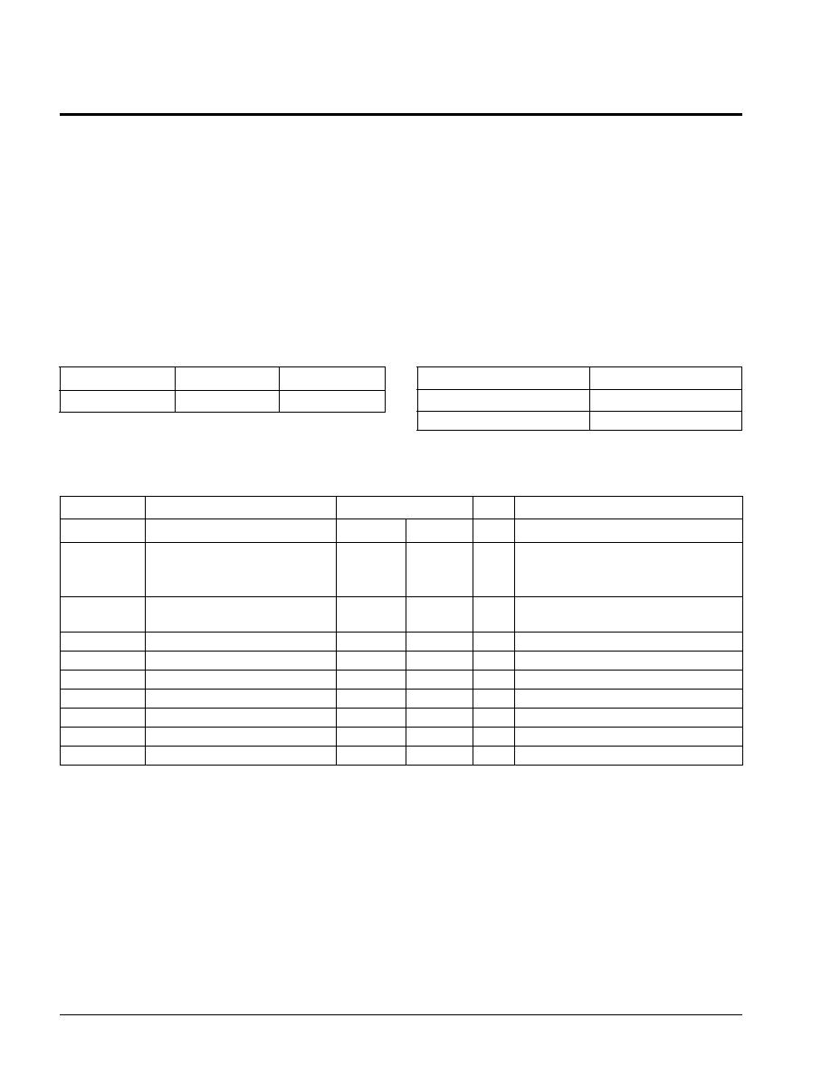
D.C. OPERATING CHARACTERISTICS (Over recommended operating conditions, unless otherwise specified.)
Limits
Symbol
Parameter
Min.
Max.
Units
Test Conditions
I
CC
V
CC
Current (Active)
50
mA
CE
=
OE
= V
IL
,
WE
= V
IH
,
(TTL Inputs)
All I/O's = Open, Address Inputs =
.4V/2.4V Levels @ f = 5MHz
I
SB1
V
CC
Current (Standby)
3
mA
CE
= V
IH
,
OE
= V
IL
(TTL Inputs)
All I/O's = Open, Other Inputs = V
CC
I
LI
Input Leakage Current
20
µ
A
V
IN
= V
SS
to V
CC
I
LO
Output Leakage Current
20
µ
A
V
OUT
= V
SS
to V
CC
,
CE
= V
IH
V
lL
(1)
Input LOW Voltage
≠1
0.6
V
V
IH
(1)
Input HIGH Voltage
2.2
V
CC
+ 1
V
V
OL
Output LOW Voltage
0.5
V
I
OL
= 1mA
V
OH
Output HIGH Voltage
2.6
V
I
OH
= ≠400
µ
A
V
BB
Back Bias Voltage
200
µ
A
V
BB
= ≠3V
±
10%
6614 PGM T04.2
ABSOLUTE MAXIMUM RATINGS*
Temperature under Bias
X28HT512 ................................. ≠40
∞
C to +175
∞
C
Voltage on any Pin with
Respect to V
SS .......................................
≠1V to +7V
D.C. Output Current ............................................. 5mA
Lead Temperature
(Soldering, 10 seconds) .............................. 300
∞
C
*COMMENT
Stresses above those listed under "Absolute Maximum
Ratings" may cause permanent damage to the device.
This is a stress rating only and the functional operation of
the device at these or any other conditions above those
indicated in the operational sections of this specification is
not implied. Exposure to absolute maximum rating condi-
tions for extended periods may affect device reliability.
RECOMMEND OPERATING CONDITIONS
Temperature
Min.
Max.
High Temp
≠40
∞
C
+175
∞
C
6614 PGM T02.1
Supply Voltage
Limits
X28HT512
5V
±
5%
Back Bias Voltage (V
BB
)
≠3V
±
10%
6614 PGM T03.1
Notes: (1) V
IL
min. and V
IH
max. are for reference only and are not tested.
X28HT512
5
POWER-UP TIMING
Symbol
Parameter
Max.
Units
t
PUR
(2)
Power-up to Read Operation
100
µ
s
t
PUW
(2)
Power-up to Write Operation
5
ms
6614 PGM T05
CAPACITANCE T
A
= +25
∞
C, f = 1MHz, V
CC
= 5V
Symbol
Parameter
Max.
Units
Test Conditions
C
I/O
(2)
Input/Output Capacitance
10
pF
V
I/O
= 0V
C
IN
(2)
Input Capacitance
10
pF
V
IN
= 0V
6614 PGM T06
ENDURANCE AND DATA RETENTION
Parameter
Min.
Max.
Units
Endurance
10,000
Cycles per Byte
Data Retention
100
Years
6614 PGM T11
A.C. CONDITIONS OF TEST
Input Pulse Levels
0V to 3V
Input Rise and
Fall Times
10ns
Input and Output
Timing Levels
1.5V
6614 PGM T07
MODE SELECTION
CE
OE
WE
Mode
I/O
Power
L
L
H
Read
D
OUT
Active
L
H
L
Write
D
IN
Active
H
X
X
Standby and
High Z
Standby
Write Inhibit
X
L
X
Write Inhibit
--
--
X
X
H
Write Inhibit
--
--
6614 PGM T08
Note:
(2) This parameter is periodically sampled and not 100%
tested.
EQUIVALENT A.C. LOAD CIRCUIT
SYMBOL TABLE
WAVEFORM
INPUTS
OUTPUTS
Must be
steady
Will be
steady
May change
from LOW
to HIGH
Will change
from LOW
to HIGH
May change
from HIGH
to LOW
Will change
from HIGH
to LOW
Don't Care:
Changes
Allowed
Changing:
State Not
Known
N/A
Center Line
is High
Impedance
6614 FHD F22.2
5V
1.92K
100pF
OUTPUT
1.37K

6
X28HT512
A.C. CHARACTERISTICS (Over the recommended operating conditions, unless otherwise specified.)
Read Cycle
Notes: (3) t
LZ
min., t
HZ
, t
OLZ
min., and tOHZ are periodically sampled and not 100% tested. t
HZ
max. and t
OHZ
max. are measured, with
C
L
= 5pF from the point when
CE
or
OE
return HIGH (whichever occurs first) to the time when the outputs are no longer driven.
Read Cycle Limits
X28HT512-20 X28HT512-25
Symbol
Parameter
Min.
Max.
Min.
Max.
Units
t
RC
Read Cycle Time
200
250
ns
t
CE
Chip Enable Access Time
200
250
ns
t
AA
Address Access Time
200
250
ns
t
OE
Output Enable Access Time
80
80
ns
t
LZ
(3)
CE
LOW to Active Output
0
0
ns
t
OLZ
(3)
OE
LOW to Active Output
0
0
ns
t
HZ
(3)
CE
HIGH to High Z Output
80
80
ns
t
OHZ
(3)
OE
HIGH to High Z Output
80
80
ns
t
OH
Output Hold from Address Change
0
0
ns
6614 PGM T09.1
6614 FHD F05
tCE
tRC
ADDRESS
CE
OE
WE
DATA VALID
DATA VALID
tOE
tLZ
tOLZ
tOH
tAA
tHZ
tOHZ
DATA I/O
VIH
HIGH Z
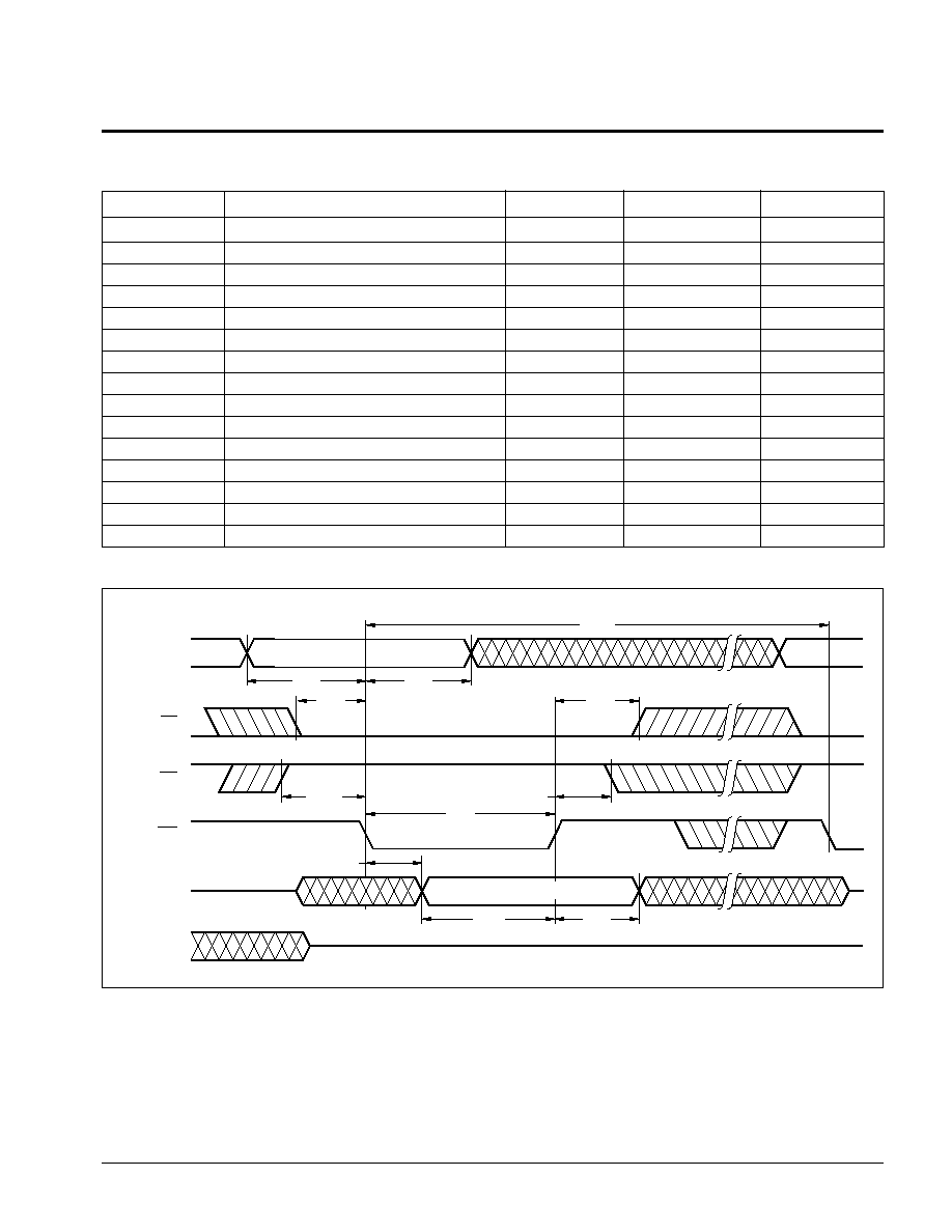
X28HT512
7
WRITE CYCLE LIMITS
Symbol
Parameter
Min.
Max.
Units
t
WC
(4)
Write Cycle Time
10
ms
t
AS
Address Setup Time
20
ns
t
AH
Address Hold Time
100
ns
t
CS
Write Setup Time
0
ns
t
CH
Write Hold Time
0
ns
t
CW
CE
Pulse Width
200
ns
t
OES
OE
HIGH Setup Time
10
ns
t
OEH
OE
HIGH Hold Time
10
ns
t
WP
WE
Pulse Width
200
ns
t
WPH
WE
HIGH Recovery
200
ns
t
DV
Data Valid
1
µ
s
t
DS
Data Setup
100
ns
t
DH
Data Hold
25
ns
t
DW
Delay to Next Write
10
µ
s
t
BLC
Byte Load Cycle
0.4
100
µ
s
6614 PGM T10.1
WE
Controlled Write Cycle
Notes: (4) t
WC
is the minimum cycle time to be allowed from the system perspective unless polling techniques are used. It is the maximum time
the device requires to complete the internal write operation.
6614 FHD F06
ADDRESS
tAS
tWC
tAH
tOES
tDV
tDS
tDH
tOEH
CE
WE
OE
DATA IN
DATA OUT
HIGH Z
tCS
tCH
tWP
DATA VALID

8
X28HT512
CE
Controlled Write Cycle
Notes: (5) Between successive byte writes within a page write operation,
OE
can be strobed LOW: e.g. this can be done with
CE
and
WE
HIGH
to fetch data from another memory device within the system for the next write; or with
WE
HIGH and
CE
LOW effectively performing
a polling operation.
(6) The timings shown above are unique to page write operations. Individual byte load operations within the page write must conform
to either the
CE
or
WE
controlled write cycle timing.
Page Write Cycle
6614 FHD F07
ADDRESS
tAS
tOEH
tWC
tAH
tOES
tWPH
tCS
tDV
tDS
tDH
tCH
CE
WE
OE
DATA IN
DATA OUT
HIGH Z
tCW
DATA VALID
6614 FHD F08
WE
OE
(5)
BYTE 0
BYTE 1
BYTE 2
BYTE n
BYTE n+1
BYTE n+2
tWP
tWPH
tBLC
tWC
CE
ADDRESS *
(6)
I/O
*For each successive write within the page write operation, A7≠A15 should be the same or
writes to an unknown address could occur.
LAST BYTE

X28HT512
9
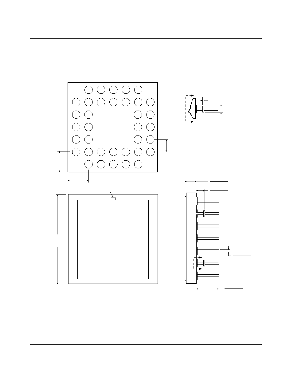
PACKAGING INFORMATION
0.620 (15.75)
0.590 (14.99)
TYP. 0.614 (15.60)
0.110 (2.79)
0.090 (2.29)
TYP. 0.018 (0.46)
1.690 (42.95)
MAX.
0.023 (0.58)
0.014 (0.36)
TYP. 0.018 (0.46)
0.232 (5.90) MAX.
0.060 (1.52)
0.015 (0.38)
3926 FHD F09
PIN 1
0.200 (5.08)
0.125 (3.18)
0.065 (1.65)
0.033 (0.84)
TYP. 0.055 (1.40)
0.610 (15.49)
0.500 (12.70)
0.100 (2.54) MAX.
0
∞
15
∞
32-LEAD HERMETIC DUAL IN-LINE PACKAGE TYPE D
NOTE: ALL DIMENSIONS IN INCHES (IN PARENTHESES IN MILLIMETERS)
0.005 (0.13) MIN.
0.150 (3.81) MIN.
0.015 (0.38)
0.008 (0.20)
SEATING
PLANE

10
X28HT512
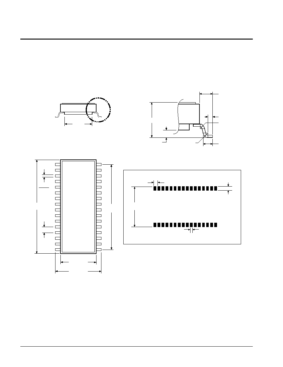
PACKAGING INFORMATION
32-LEAD CERAMIC FLAT PACK TYPE F
3926 FHD F20
NOTE: ALL DIMENSIONS IN INCHES (IN PARENTHESES IN MILLIMETERS)
0.019 (0.48)
0.015 (0.38)
0.045 (1.14) MAX.
PIN 1 INDEX
1
32
0.120 (3.05)
0.090 (2.29)
0.045 (1.14)
0.026 (0.66)
0.007 (0.18)
0.004 (0.10)
0.370 (9.40)
0.270 (6.86)
0.830 (21.08) MAX.
0.050 (1.27) BSC
0.488
0.430 (10.93)
0.347 (8.82)
0.330 (8.38)
0.005 (0.13) MIN.
0.030 (0.76)
MIN
1.228 (31.19)
1.000 (25.40)
X28HT512
11
PACKAGING INFORMATION
3926 FHD F21
36-LEAD CERAMIC PIN GRID ARRAY PACKAGE TYPE K
15
17
19
21
22
14
16
18
20
23
10
9
27
28
8
7
29
30
5
2
36
34
32
4
3
1
35
33
TYP. 0.100 (2.54)
ALL LEADS
PIN 1 INDEX
0.050 (1.27)
0.008 (0.20)
NOTE: LEADS 5, 14, 23, & 32
12
11
25
26
13
6
31
24
A
A
TYP. 0.180 (.010)
(4.57
±
.25)
4 CORNERS
0.770 (19.56)
0.750 (19.05)
SQ
A
A
0.185 (4.70)
0.175 (4.45)
0.020 (0.51)
0.016 (0.41)
0.072 (1.83)
0.062 (1.57)
0.120 (3.05)
0.100 (2.54)
NOTE: ALL DIMENSIONS IN INCHES (IN PARENTHESES IN MILLIMETERS)
TYP. 0.180 (.010)
(4.57
±
.25)
4 CORNERS
12
X28HT512
32-LEAD CERAMIC SMALL OUTLINE GULL WING PACKAGE TYPE R
3926 FHD F27
NOTES:
1. ALL DIMENSIONS IN INCHES
2. FORMED LEAD SHALL BE PLANAR WITH RESPECT TO ONE ANOTHER WITHIN 0.004 INCHES
0.340
±
0.007
SEE DETAIL "A"
FOR LEAD
INFORMATION
0.440 MAX.
0.560 NOM.
0.0192
0.0138
0.050
0.750
±
0.005
0.840
MAX.
0.060 NOM.
0.020 MIN.
0.015 R TYP.
0.035 MIN.
0.015 R
TYP.
0.035 TYP.
0.165 TYP.
DETAIL "A"
0.560"
TYPICAL
0.050"
TYPICAL
0.050"
TYPICAL
FOOTPRINT
0.030" TYPICAL
32 PLACES
PACKAGING INFORMATION

X28HT512
13
LIMITED WARRANTY
Devices sold by Xicor, Inc. are covered by the warranty and patent indemnification provisions appearing in its Terms of Sale only. Xicor, Inc. makes
no warranty, express, statutory, implied, or by description regarding the information set forth herein or regarding the freedom of the described
devices from patent infringement. Xicor, Inc. makes no warranty of merchantability or fitness tor any purpose. Xicor, Inc. reserves the right to
discontinue production and change specifications and prices at any time and without notice.
Xicor, Inc. assumes no responsibility for the use of any circuitry other than circuitry embodied in a Xicor, Inc. product. No other circuits, patents,
licenses are implied.
US. PATENTS
Xicor products are covered by one or more of the following U.S. Patents: 4,263,664; 4,274,012; 4,300,212; 4,314,265; 4,326,134; 4,393,481;
4,404,475; 4,450,402; 4,486,769; 4,488,060; 4,520,461; 4,533,846; 4,599,706; 4,617,652; 4,668,932; 4,752,912; 4,829,482; 4,874,967; 4,883,976.
Foreign patents and additional patents pending.
LIFE RELATED POLICY
In situations where semiconductor component failure may endanger life, system designers using this product should design the system with
appropriate error detection and correction, redundancy and back-up features to prevent such an occurrence.
Xicor's products are not authorized for use as critical components in life support devices or systems.
1. Life support devices or systems are devices or systems which, (a) are intended for surgical implant into the body, or (b) support or sustain life,
and whose failure to perform, when properly used in accordance with instructions for use provided in the labeling, can be reasonably expected
to result in a significant injury to the user.
2. A critical component is any component of a life support device or system whose failure to perform can be reasonably expected to cause the failure
of the life support device or system, or to affect its satety or effectiveness.
ORDERING INFORMATION
Device
Access Time
≠25 = 250ns
≠20 = 200ns
Temperature Range
Blank = 25
∞
C to +175
∞
C
Package
D = 32-Lead CerDip
F = 32-Lead Flat Pack
K = 36-Lead Pin Grid Array
R = 32-Lead Ceramic SOIC
X28HT512 X
X
-X