Document Outline
- Table of Contents
- Product Selection
- Data Sheet Alpha
- Ap Note Alpha
X28VC256
1
©Xicor, Inc. 1991, 1995 Patents Pending
Characteristics subject to change without notice
3869-2.6 4/2/96 T4/C4/D0 NS
5 Volt, Byte Alterable E
2
PROM
FEATURES
∑
Access Time: 45ns
∑
Simple Byte and Page Write
--Single 5V Supply
-- No External High Voltages or V
PP
Control
Circuits
--Self-Timed
-- No Erase Before Write
-- No Complex Programming Algorithms
--No Overerase Problem
∑
Low Power CMOS:
--Active: 80mA
--Standby: 10mA
∑
Software Data Protection
--Protects Data Against System Level
Inadvertent Writes
∑
High Speed Page Write Capability
∑
Highly Reliable Direct Write
TM
Cell
--Endurance: 100,000 Write Cycles
--Data Retention: 100 Years
∑
Early End of Write Detection
--
DATA
Polling
--Toggle Bit Polling
DESCRIPTION
The X28VC256 is a second generation high perfor-
mance CMOS 32K x 8 E
2
PROM. It is fabricated with
Xicor's proprietary, textured poly floating gate tech-
nology, providing a highly reliable 5 Volt only nonvolatile
memory.
The X28VC256 supports a 128-byte page write opera-
tion, effectively providing a 24
µ
s/byte write cycle and
enabling the entire memory to be typically rewritten in
less than 0.8 seconds. The X28VC256 also features
DATA
Polling and Toggle Bit Polling, two methods of
providing early end of write detection. The X28VC256
also supports the JEDEC standard Software Data Pro-
tection feature for protecting against inadvertent writes
during power-up and power-down.
Endurance for the X28VC256 is specified as a minimum
100,000 write cycles per byte and an inherent data
retention of 100 years.
256K
X28VC256
32K x 8 Bit
PIN CONFIGURATION
A14
A12
A7
A6
A5
A4
A3
A2
A1
A0
I/O0
I/O1
I/O2
VSS
1
2
3
4
5
6
7
8
9
10
11
12
13
14
28
27
26
25
24
23
22
21
20
19
18
17
16
15
VCC
WE
A13
A8
A9
A11
OE
A10
CE
I/O7
I/O6
I/O5
I/04
I/O3
X28VC256
3869 FHD F02
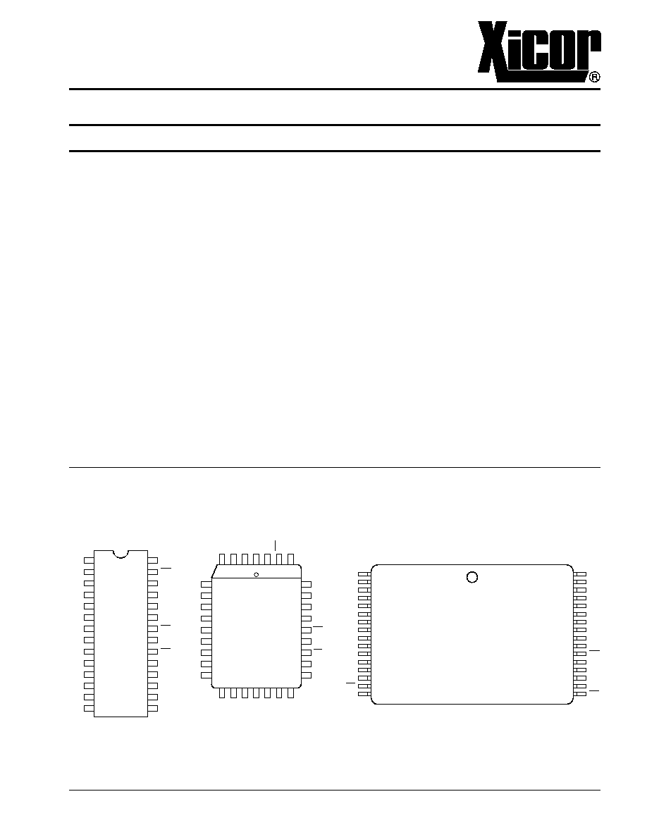
PLASTIC DIP
CERDIP
FLAT PACK
SOIC
1
2
3
4
5
6
7
8
9
10
11
12
13
14
15
16
X28VC256
A3
A4
A5
A6
A7
A12
A14
NC
VCC
NC
WE
A13
A8
A9
A11
OE
32
31
30
29
28
27
26
25
24
23
22
21
20
19
18
17
A2
A1
A0
I/O0
I/O1
I/O2
NC
VSS
NC
I/O3
I/O4
I/O5
I/O6
I/O7
CE
A10
TSOP
A6
A5
A4
A3
A2
A1
A0
NC
I/O0
A8
A9
A11
NC
OE
A10
CE
I/O7
I/O6
4
3
2
1 32 31 30
14 15 16 17 18 19 20
5
6
7
8
9
10
11
12
13
29
28
27
26
25
24
23
22
21
X28VC256
A
7
A
12
A
14
NC
V
CC
WE
A
13
I/O
1
I/O
2
V
SS
NC
I/O
3
I/O
4
I/O
5
LCC
PLCC
3869 FHD F03
3869 ILL F22
X28VC256
2
PIN DESCRIPTIONS
Addresses (A
0
≠A
14
)
The Address inputs select an 8-bit memory location
during a read or write operation.
Chip Enable (
CE
)
The Chip Enable input must be LOW to enable all read/
write operations. When
CE
is HIGH, power consumption
is reduced.
Output Enable (
OE
)
The Output Enable input controls the data output buffers
and is used to initiate read operations.
Data In/Data Out (I/O
0
≠I/O
7
)
Data is written to or read from the X28VC256 through the
I/O pins.
Write Enable (
WE
)
The Write Enable input controls the writing of data to the
X28VC256.
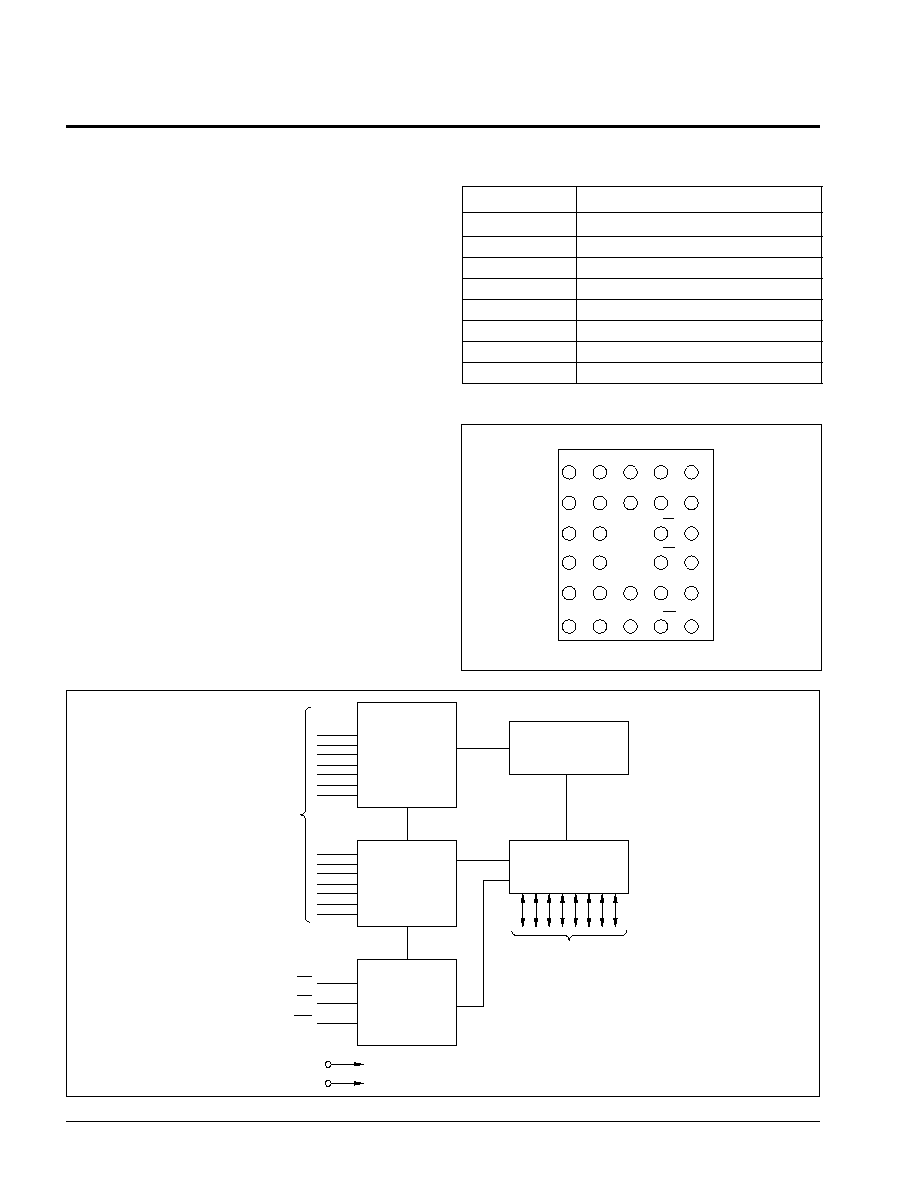
X BUFFERS
LATCHES AND
DECODER
I/O BUFFERS
AND LATCHES
3869 FHD F01
Y BUFFERS
LATCHES AND
DECODER
CONTROL
LOGIC AND
TIMING
256K-BIT
E2PROM
ARRAY
I/O0≠I/O7
DATA INPUTS/OUTPUTS
CE
OE
VCC
VSS
A0≠A14
ADDRESS
INPUTS
WE
3869 FHD F01
FUNCTIONAL DIAGRAM
PIN NAMES
Symbol
Description
A
0
≠A
14
Address Inputs
I/O
0
≠I/O
7
Data Input/Output
WE
Write Enable
CE
Chip Enable
OE
Output Enable
V
CC
+5V
V
SS
Ground
NC
No Connect
3869 PGM T01
PGA
3869 FHD F04
PIN CONFIGURATION
11
I/O0
10
A0
14
VSS
9
A1
8
A2
7
A3
6
A4
5
A5
2
A12
28
VCC
12
I/O1
13
I/O2
15
I/O3
4
A6
3
A7
1
16
I/O4
20
CE
22
OE
24
A9
17
I/O5
27
WE
19
I/O7
21
A10
23
A11
25
A8
18
I/O6
26
A13
X28VC256
(BOTTOM VIEW)
A14
X28VC256
3
DEVICE OPERATION
Read
Read operations are initiated by both
OE
and
CE
LOW.
The read operation is terminated by either
CE
or
OE
returning HIGH. This two line control architecture elimi-
nates bus contention in a system environment. The data
bus will be in a high impedance state when either
OE
or
CE
is HIGH.
Write
Write operations are initiated when both
CE
and
WE
are
LOW and
OE
is HIGH. The X28VC256 supports both a
CE
and
WE
controlled write cycle. That is, the address
is latched by the falling edge of either
CE
or
WE
,
whichever occurs last. Similarly, the data is latched
internally by the rising edge of either
CE
or
WE
,
whichever occurs first. A byte write operation, once
initiated, will automatically continue to completion, typi-
cally within 3ms.
Page Write Operation
The page write feature of the X28VC256 allows the
entire memory to be written in typically 0.8 seconds.
Page write allows up to one hundred twenty-eight bytes
of data to be consecutively written to the X28VC256
prior to the commencement of the internal programming
cycle. The host can fetch data from another device
within the system during a page write operation (change
the source address), but the page address (A
7
through
A
14
) for each subsequent valid write cycle to the part
during this operation must be the same as the initial
page address.
The page write mode can be initiated during any write
operation. Following the initial byte write cycle, the host
can write an additional one to one hundred twenty-
seven bytes in the same manner as the first byte was
written. Each successive byte load cycle, started by the
WE
HIGH to LOW transition, must begin within 100
µ
s of
the falling edge of the preceding
WE
. If a subsequent
WE
HIGH to LOW transition is not detected within
100
µ
s, the internal automatic programming cycle will
commence. There is no page write window limitation.
Effectively the page write window is infinitely wide, so
long as the host continues to access the device within
the byte load cycle time of 100
µ
s.
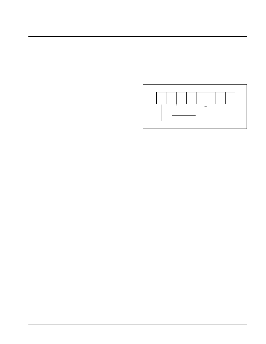
Write Operation Status Bits
The X28VC256 provides the user two write operation
status bits. These can be used to optimize a system write
cycle time. The status bits are mapped onto the I/O bus as
shown in Figure 1.
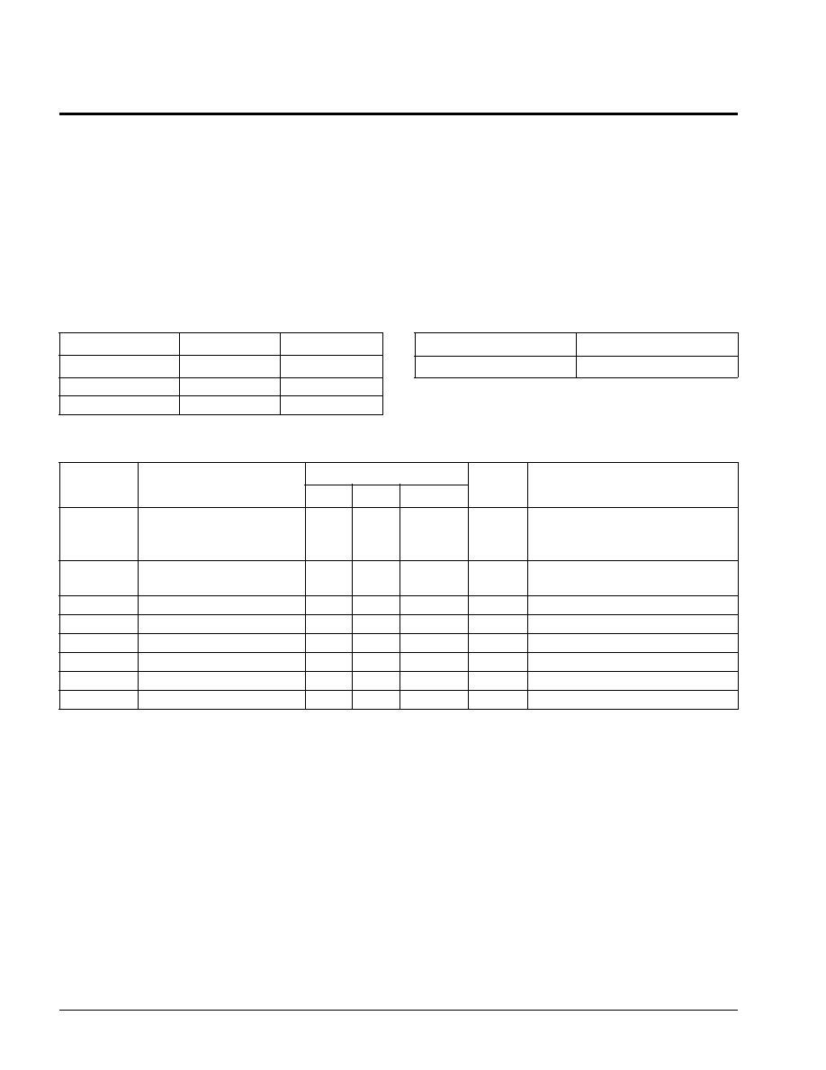
Figure 1. Status Bit Assignment
3869 FHD F11
DATA
Polling (I/O
7
)
The X28VC256 features
DATA
Polling as a method to
indicate to the host system that the byte write or page
write cycle has completed.
DATA
Polling allows a simple
bit test operation to determine the status of the
X28VC256, eliminating additional interrupt inputs or
external hardware. During the internal programming
cycle, any attempt to read the last byte written will
produce the complement of that data on I/O
7
(i.e., write
data = 0xxx xxxx, read data = 1xxx xxxx). Once the
programming cycle is complete, I/O
7
will reflect true
data.
Toggle Bit (I/O
6
)
The X28VC256 also provides another method for deter-
mining when the internal write cycle is complete. During
the internal programming cycle I/O
6
will toggle from
HIGH to LOW and LOW to HIGH on subsequent at-
tempts to read the device. When the internal cycle is
complete the toggling will cease and the device will be
accessible for additional read and write operations.
5
TB
DP
4
3
2
1
0
I/O
RESERVED
TOGGLE BIT
DATA POLLING

X28VC256
4
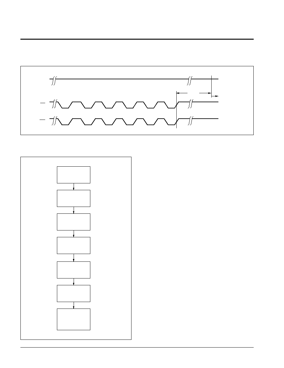
DATA
POLLING I/O
7
Figure 2.
DATA
Polling Bus Sequence
3869 FHD F12
Figure 3.
DATA
Polling Software Flow
DATA
Polling can effectively halve the time for writing to
the X28VC256. The timing diagram in Figure 2 illus-
trates the sequence of events on the bus. The software
flow diagram in Figure 3 illustrates one method of
implementing the routine.
3869 FHD F13
WRITE DATA
SAVE LAST DATA
AND ADDRESS
READ LAST
ADDRESS
IO7
COMPARE?
X28VC256
READY
NO
YES
WRITES
COMPLETE?
NO
YES
CE
OE
WE
I/O7
X28VC256
READY
LAST
WRITE
HIGH Z
VOL
VIH
A0≠A14
An
An
An
An
An
An
VOH
An

X28VC256
5
THE TOGGLE BIT I/O
6
Figure 4. Toggle Bit Bus Sequence
3869 FHD F14
Figure 5. Toggle Bit Software Flow
The Toggle Bit can eliminate the software housekeeping
chore of saving and fetching the last address and data
written to a device in order to implement
DATA
Polling.
This can be especially helpful in an array comprised of
multiple X28VC256 memories that is frequently up-
dated. The timing diagram in Figure 4 illustrates the
sequence of events on the bus. The software flow
diagram in Figure 5 illustrates a method for polling the
Toggle Bit.
3869 FHD F15
LOAD ACCUM
FROM ADDR n
COMPARE
ACCUM WITH
ADDR n
X28VC256
READY
COMPARE
OK?
NO
YES
LAST WRITE
YES
CE
OE
WE
I/O6
X28VC256
READY
VOH
VOL
LAST
WRITE
HIGH Z
* I/O6 beginning and ending state of I/O6 will vary.
*
*

X28VC256
6
circuits by employing the software data protection fea-
ture. The internal software data protection circuit is
enabled after the first write operation utilizing the soft-
ware algorithm. This circuit is nonvolatile and will remain
set for the life of the device unless the reset command
is issued.
Once the software protection is enabled, the X28VC256
is also protected from inadvertent and accidental writes
in the powered-up state. That is, the software algorithm
must be issued prior to writing additional data to the
device.
SOFTWARE ALGORITHM
Selecting the software data protection mode requires
the host system to precede data write operations by a
series of three write operations to three specific ad-
dresses. Refer to Figure 6 and 7 for the sequence. The
three-byte sequence opens the page write window
enabling the host to write from one to one hundred
twenty-eight bytes of data. Once the page load cycle has
been completed, the device will automatically be re-
turned to the data protected state.
HARDWARE DATA PROTECTION
The X28VC256 provides two hardware features that
protect nonvolatile data from inadvertent writes.
∑
Default V
CC
Sense--All write functions are inhibited
when V
CC
is
3.5V typically.
∑
Write Inhibit--Holding either
OE
LOW,
WE
HIGH, or
CE
HIGH will prevent an inadvertent write cycle during
power-up and power-down, maintaining data integrity.
SOFTWARE DATA PROTECTION
The X28VC256 offers a software controlled data protec-
tion feature. The X28VC256 is shipped from Xicor with
the software data protection NOT ENABLED; that is, the
device will be in the standard operating mode. In this
mode data should be protected during power-up/down
operations through the use of external circuits. The host
would then have open read and write access of the
device once V
CC
was stable.
The X28VC256 can be automatically protected during
power-up and power-down without the need for external

X28VC256
7
SOFTWARE DATA PROTECTION
Figure 6. Timing Sequence--Byte or Page Write
3869 FHD F16
Figure 7. Write Sequence for
Software Data Protection
Regardless of whether the device has previously been
protected or not, once the software data protection
algorithm is used and data has been written, the
X28VC256 will automatically disable further writes un-
less another command is issued to cancel it. If no further
commands are issued the X28VC256 will be write
protected during power-down and after any subsequent
power-up.
Note:
Once initiated, the sequence of write operations
should not be interrupted.
3869 FHD F17
CE
WE
(VCC)
WRITE
PROTECTED
VCC
0V
DATA
ADDRESS
AA
5555
55
2AAA
A0
5555
tBLC MAX
WRITES
OK
BYTE
OR
PAGE
tWC
tBLC MAX
WRITE LAST
BYTE TO
LAST ADDRESS
WRITE DATA 55
TO ADDRESS
2AAA
WRITE DATA A0
TO ADDRESS
5555
WRITE DATA XX
TO ANY
ADDRESS
AFTER tWC
RE-ENTERS DATA
PROTECTED STATE
WRITE DATA AA
TO ADDRESS
5555
BYTE/PAGE
LOAD ENABLED
OPTIONAL
BYTE OR
PAGE WRITE
ALLOWED
X28VC256
8
Figure 9. Write Sequence for Resetting
Software Data Protection
RESETTING SOFTWARE DATA PROTECTION
Figure 8. Reset Software Data Protection Timing Sequence
3869 FHD F18
In the event the user wants to deactivate the software
data protection feature for testing or reprogramming in
an E
2
PROM programmer, the following six step algo-
rithm will reset the internal protection circuit. After t
WC
,
the X28VC256 will be in standard operating mode.
Note:
Once initiated, the sequence of write operations
should not be interrupted.
3869 FHD F19
CE
WE
STANDARD
OPERATING
MODE
VCC
DATA
ADDRESS
AA
5555
55
2AAA
80
5555
tWC
AA
5555
55
2AAA
20
5555
WRITE DATA 55
TO ADDRESS
2AAA
WRITE DATA 55
TO ADDRESS
2AAA
WRITE DATA 80
TO ADDRESS
5555
WRITE DATA AA
TO ADDRESS
5555
WRITE DATA 20
TO ADDRESS
5555
WRITE DATA AA
TO ADDRESS
5555
AFTER tWC,
RE-ENTERS
UNPROTECTED
STATE

X28VC256
9
prime concern. Enabling
CE
will cause transient current
spikes. The magnitude of these spikes is dependent on
the output capacitive loading of the l/Os. Therefore, the
larger the array sharing a common bus, the larger the
transient spikes. The voltage peaks associated with the
current transients can be suppressed by the proper
selection and placement of decoupling capacitors. As a
minimum, it is recommended that a 0.1
µ
F high fre-
quency ceramic capacitor be used between V
CC
and
V
SS
at each device. Depending on the size of the array,
the value of the capacitor may have to be larger.
In addition, it is recommended that a 4.7
µ
F electrolytic
bulk capacitor be placed between V
CC
and V
SS
for each
eight devices employed in the array. This bulk capacitor
is employed to overcome the voltage droop caused by
the inductive effects of the PC board traces.
SYSTEM CONSIDERATIONS
Because the X28VC256 is frequently used in large
memory arrays it is provided with a two line control
architecture for both read and write operations. Proper
usage can provide the lowest possible power dissipation
and eliminate the possibility of contention where mul-
tiple I/O pins share the same bus.
To gain the most benefit it is recommended that
CE
be
decoded from the address bus and be used as the
primary device selection input. Both
OE
and
WE
would
then be common among all devices in the array. For a
read operation this assures that all deselected devices
are in their standby mode and that only the selected
device(s) is outputting data on the bus.
Because the X28VC256 has two power modes, standby
and active, proper decoupling of the memory array is of
X28VC256
10
*COMMENT
Stresses above those listed under "Absolute Maximum
Ratings" may cause permanent damage to the device.
This is a stress rating only and the functional operation of
the device at these or any other conditions above those
indicated in the operational sections of this specification is
not implied. Exposure to absolute maximum rating condi-
tions for extended periods may affect device reliability.
ABSOLUTE MAXIMUM RATINGS*
Temperature under Bias
X28VC256 .................................. ≠10
∞
C to +85
∞
C
X28VC256I, X28VC256M .......... ≠65
∞
C to +135
∞
C
Storage Temperature ....................... ≠65
∞
C to +150
∞
C
Voltage on any Pin with
Respect to V
SS
.................................. ≠1V to +7V
D.C. Output Current ........................................... 10mA
Lead Temperature (Soldering, 10 seconds) ...... 300
∞
C
RECOMMENDED OPERATING CONDITIONS
Temperature
Min.
Max.
Commercial
0
∞
C
+70
∞
C
Industrial
≠40
∞
C
+85
∞
C
Military
≠55
∞
C
+125
∞
C
3869 PGM T02.1
Supply Voltage
Limits
X28VC256
5V
±
10%
3869 PGM T03.1
D.C. OPERATING CHARACTERISTICS (Over recommended operating conditions unless otherwise specified.)
Limits
Symbol
Parameter
Min.
Typ.
(1)
Max.
Units
Test Conditions
I
CC
V
CC
Active Current
30
80
mA
CE
=
OE
= V
IL
,
WE
= V
IH
,
All I/O's = Open, Address Inputs =
0.4V/2.4V Levels @ f = 10MHz
I
SB
V
CC
Standby Current
10
25
mA
CE
= V
IH
,
OE
= V
IL
, All I/O's =
Open, Other Inputs = V
IH
I
LI
Input Leakage Current
10
µ
A
V
IN
= V
SS
to V
CC
I
LO
Output Leakage Current
10
µ
A
V
OUT
= V
SS
to V
CC
,
CE
= V
IH
V
lL(2)
Input LOW Voltage
≠1
0.8
V
V
IH(2)
Input HIGH Voltage
2
V
CC
+ 1
V
V
OL
Output LOW Voltage
0.4
V
I
OL
= 6mA
V
OH
Output HIGH Voltage
2.4
V
I
OH
= ≠4mA
3869 PGM T04.2
Notes: (1) Typical values are for T
A
= 25
∞
C and nominal supply voltage.
(2) V
IL
min. and V
IH
max. are for reference only and are not tested.
X28VC256
11
POWER-UP TIMING
Symbol
Parameter
Max.
Units
t
PUR(3)
Power-Up to Read
100
µ
s
t
PUW(3)
Power-Up to Write
5
ms
3869 PGM T05
CAPACITANCE T
A
= +25
∞
C, f = 1MH
Z
, V
CC
= 5V.
Symbol
Test
Max.
Units
Conditions
C
I/O(3)
Input/Output Capacitance
10
pF
V
I/O
= 0V
C
IN(3)
Input Capacitance
6
pF
V
IN
= 0V
3869 PGM T06.1
ENDURANCE AND DATA RETENTION
Parameter
Min.
Max.
Units
Endurance
100,000
Cycles
Data Retention
100
Years
3869 PGM T07.3
MODE SELECTION
CE
OE
WE
Mode
I/O
Power
L
L
H
Read
D
OUT
Active
L
H
L
Write
D
IN
Active
H
X
X
Standby and Write Inhibit
High Z Standby
X
L
X
Write Inhibit
--
--
X
X
H
Write Inhibit
--
--
3869 PGM T09
A.C. CONDITIONS OF TEST
Input Pulse Levels
0V to 3V
Input Rise and
Fall Times
5ns
Input and Output
Timing Levels
1.5V
3869 PGM T08.1
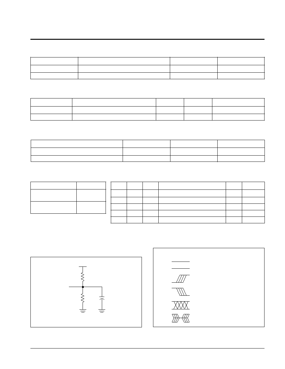
EQUIVALENT A.C. LOAD CIRCUIT
SYMBOL TABLE
WAVEFORM
INPUTS
OUTPUTS
Must be
steady
Will be
steady
May change
from LOW
to HIGH
Will change
from LOW
to HIGH
May change
from HIGH
to LOW
Will change
from HIGH
to LOW
Don't Care:
Changes
Allowed
Changing:
State Not
Known
N/A
Center Line
is High
Impedance
Note:
(3) This parameter is periodically sampled and not 100%
tested.
3869 FHD F20.3
5V
1.92K
30pF
OUTPUT
1.37K
X28VC256
12
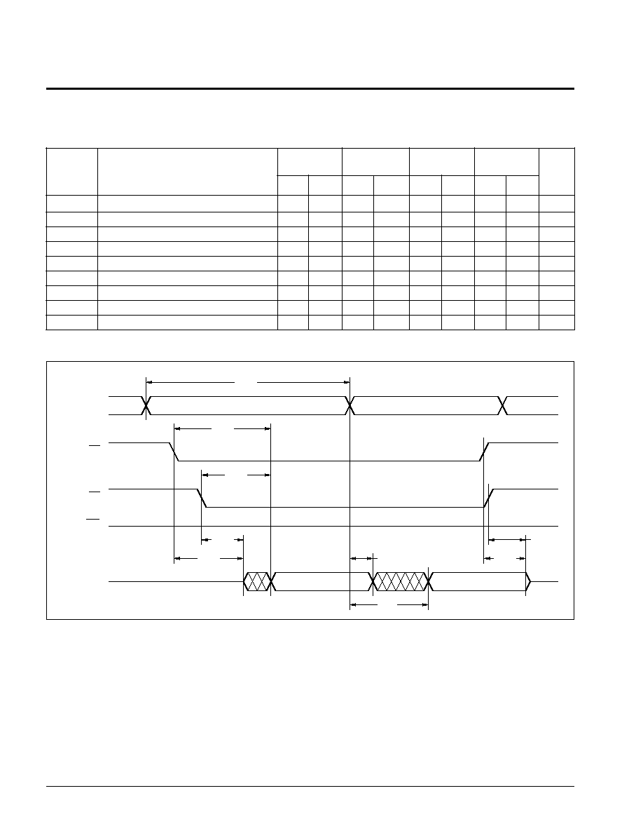
A.C. CHARACTERISTICS (Over the recommended operating conditions, unless otherwise specified.)
Read Cycle Limits
X28VC256-45
X28VC256-55
X28VC256-70 X28VC256-90
≠40
∞
C to 85
∞
C
≠55
∞
C to 125
∞
C ≠55
∞
C to 125
∞
C ≠55
∞
C to 125
∞
C
Symbol
Parameter
Min. Max.
Min. Max.
Min. Max.
Min.
Max. Units
t
RC
Read Cycle Time
45
55
70
90
ns
t
CE
Chip Enable Access Time
45
55
70
90
ns
t
AA
Address Access Time
45
55
70
90
ns
t
OE
Output Enable Access Time
30
30
35
40
ns
t
LZ
(4)
CE
LOW to Active Output
0
0
0
0
ns
t
OLZ (4)
OE
LOW to Active Output
0
0
0
0
ns
t
HZ
(4)
CE
HIGH to High Z Output
30
30
35
40
ns
t
OHZ (4)
OE
HIGH to High Z Output
30
30
35
40
ns
t
OH
Output Hold From Address Change
0
0
0
0
ns
3869 PGM T10.1
Read Cycle
3869 FHD F05
Notes: (4)
t
LZ
min., t
HZ
, t
OLZ
min. and t
OHZ
are periodically sampled and not 100% tested, t
HZ
and t
OHZ
are measured, with CL = 5pF,
from the point whin
CE
,
OE
return HIGH (whichever occurs first) to the time when the outputs are no longer driven.
tCE
tRC
ADDRESS
CE
OE
WE
DATA VALID
DATA VALID
tOE
tLZ
tOLZ
tOH
tAA
tHZ
tOHZ
DATA I/O
VIH
HIGH Z
X28VC256
13
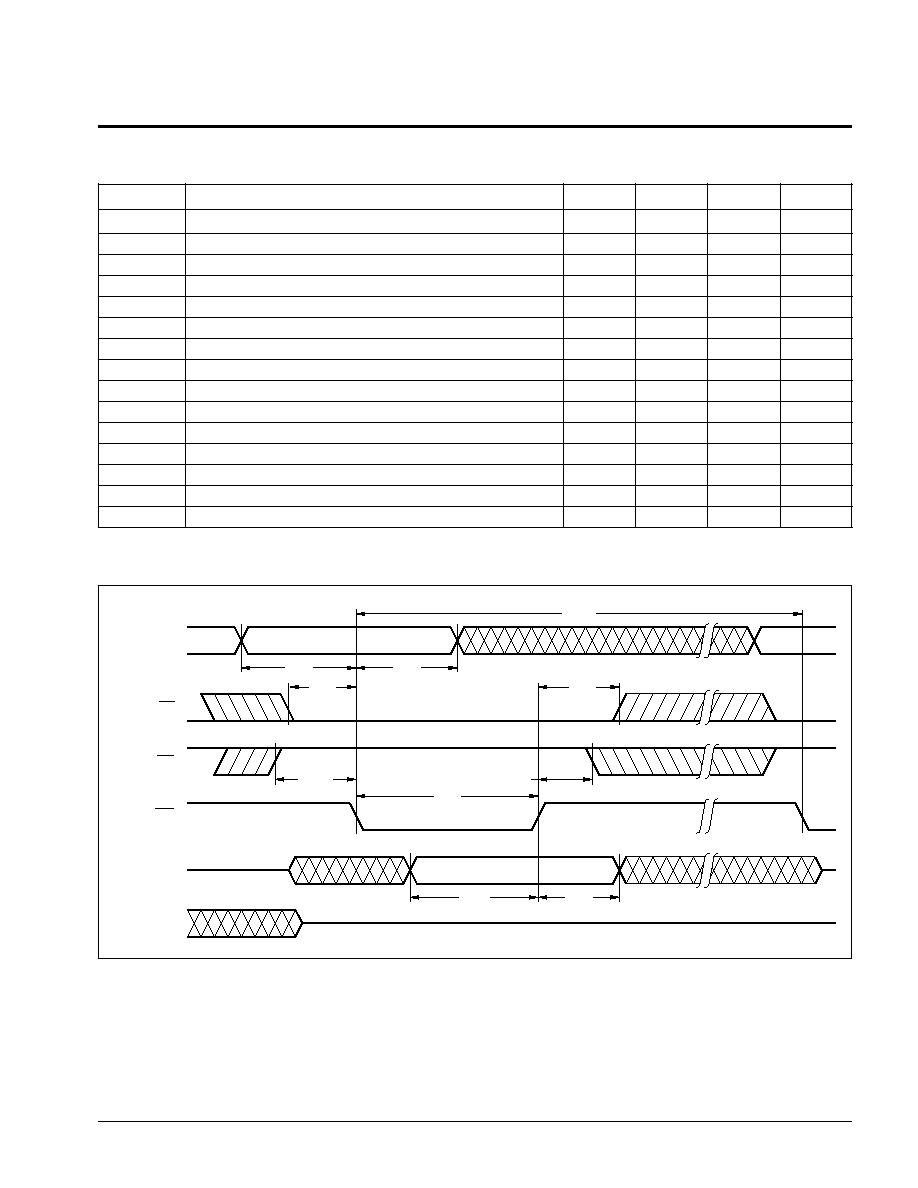
Write Cycle Limits
Symbol
Parameter
Min.
Typ.
(5)
Max.
Units
t
WC(6)
Write Cycle Time
3
5
ms
t
AS
Address Setup Time
0
ns
t
AH
Address Hold Time
50
ns
t
CS
Write Setup Time
0
ns
t
CH
Write Hold Time
0
ns
t
CW
CE
Pulse Width
50
ns
t
OES
OE
HIGH Setup Time
0
ns
t
OEH
OE
HIGH Hold Time
0
ns
t
WP
WE
Pulse Width
50
ns
t
WPH(7)
WE
HIGH Recovery (page write only)
50
ns
t
DV
Data Valid
1
µ
s
t
DS
Data Setup
50
ns
t
DH
Data Hold
0
ns
t
DW(7)
Delay to Next Write after Polling is True
10
µ
s
t
BLC
Byte Load Cycle
0.150
100
µ
s
3869 PGM T11.2
WE
Controlled Write Cycle
3869 FHD F06
Notes: (5) Typical values are for T
A
= 25
∞
C and nominal supply voltage.
(6) t
WC
is the minimum cycle time to be allowed from the system perspective unless polling techniques are used. It is the maximum
time the device requires to automatically complete the internal write operation.
(7) t
WPH
and t
DW
are periodically sampled and not 100% tested.
ADDRESS
tAS
tWC
tAH
tOES
tDS
tDH
tOEH
CE
WE
OE
DATA IN
DATA OUT
HIGH Z
DATA VALID
tCS
tCH
tWP

X28VC256
14
CE
Controlled Write Cycle
3869 FHD F07
Page Write Cycle
3869 FHD F08
Notes: (8) Between successive byte writes within a page write operation,
OE
can be strobed LOW: e.g. this can be done with
CE
and
WE
HIGH to fetch data from another memory device within the system for the next write; or with
WE
HIGH and
CE
LOW effectively
performing a polling operation.
(9) The timings shown above are unique to page write operations. Individual byte load operations within the page write must conform
to either the
CE
or
WE
controlled write cycle timing.
ADDRESS
tAS
tWC
tAH
tOES
tCS
tDS
tDH
tCH
CE
WE
OE
DATA IN
DATA OUT
HIGH Z
DATA VALID
tCW
tOEH
WE
OE
(8)
BYTE 0
BYTE 1
BYTE 2
BYTE n
BYTE n+1
BYTE n+2
tWP
tWPH
tBLC
tWC
CE
ADDRESS*
(9)
I/O
*For each successive write within the page write operation, A7≠A14 should be the same or
writes to an unknown address could occur.
LAST BYTE

X28VC256
15
DATA
Polling Timing Diagram
(10)
3869 FHD F09
Toggle Bit Timing Diagram
(10)
CE
OE
WE
I/O6
tOES
tDW
tWC
tOEH
HIGH Z
*
*
* I/O6 beginning and ending state will vary, depending upon actual tWC
ADDRESS
AN
DIN=X
DOUT=X
DOUT=X
tWC
tOEH
tOES
AN
AN
CE
WE
OE
I/O7
tDW
3869 FHD F10
Note:
(10) Polling operations are by definition read cycles and are therefore subject to read cycle timings.
X28VC256
16
PACKAGING INFORMATION
0.020 (0.51)
0.016 (0.41)
0.150 (3.81)
0.125 (3.17)
0.610 (15.49)
0.590 (14.99)
0.110 (2.79)
0.090 (2.29)
1.460 (37.08)
1.400 (35.56)
1.300 (33.02)
REF.
PIN 1 INDEX
0.160 (4.06)
0.125 (3.17)
0.030 (0.76)
0.015 (0.38)
3926 FHD F04
PIN 1
SEATING
PLANE
0.062 (1.57)
0.050 (1.27)
0.550 (13.97)
0.510 (12.95)
0.085 (2.16)
0.040 (1.02)
0
∞
15
∞
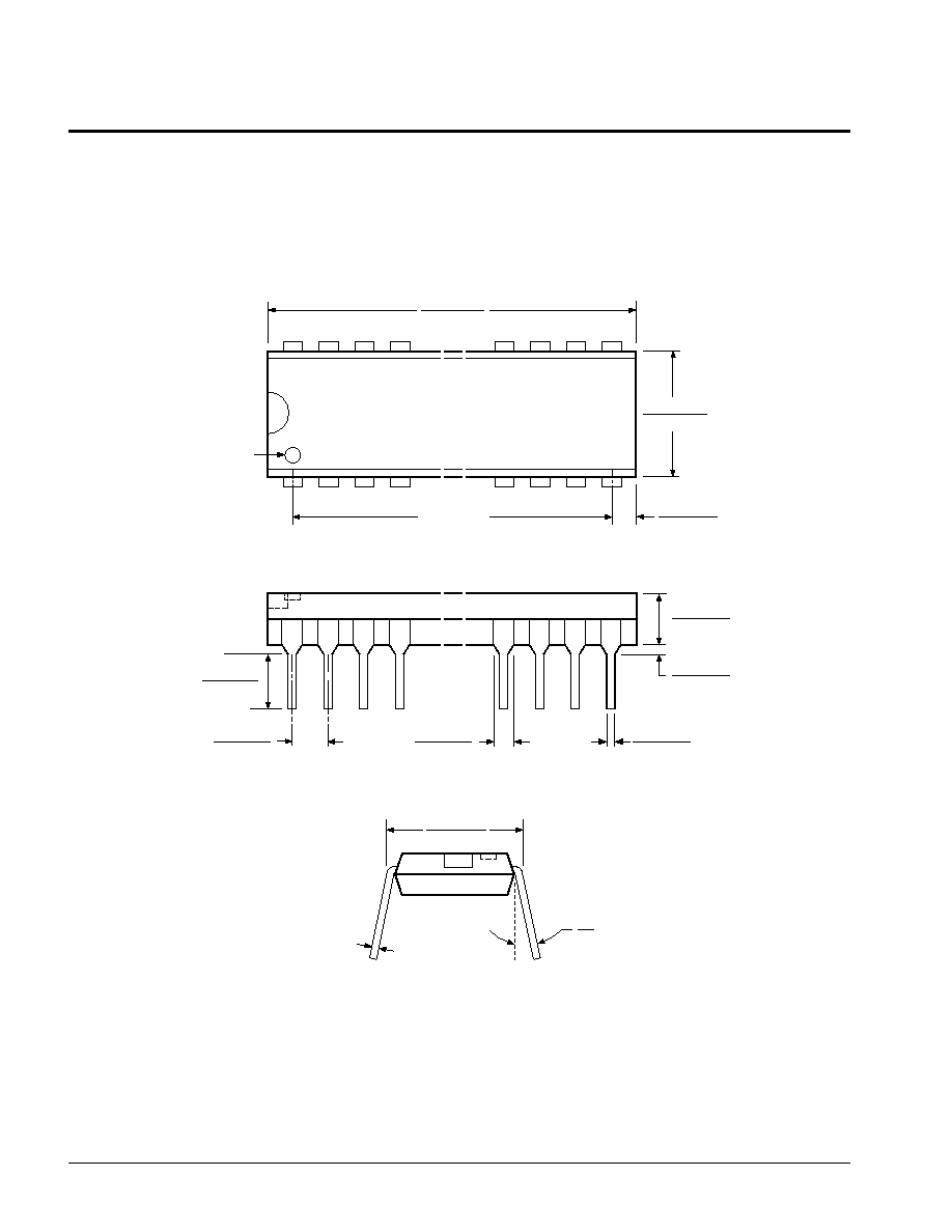
28-LEAD PLASTIC DUAL IN-LINE PACKAGE TYPE P
NOTE: ALL DIMENSIONS IN INCHES (IN PARENTHESES IN MILLIMETERS)
TYP. 0.010 (0.25)
X28VC256
17
0.620 (15.75)
0.590 (14.99)
TYP. 0.614 (15.60)
0.110 (2.79)
0.090 (2.29)
TYP. 0.100 (2.54)
0.023 (0.58)
0.014 (0.36)
TYP. 0.018 (0.46)
0.060 (1.52)
0.015 (0.38)
3926 FHD F08
PIN 1
0.200 (5.08)
0.125 (3.18)
0.065 (1.65)
0.038 (0.97)
TYP. 0.055 (1.40)
0.610 (15.49)
0.500 (12.70)
0.100 (2.54) MAX.
0.015 (0.38)
0.008 (0.20)
0
∞
15
∞
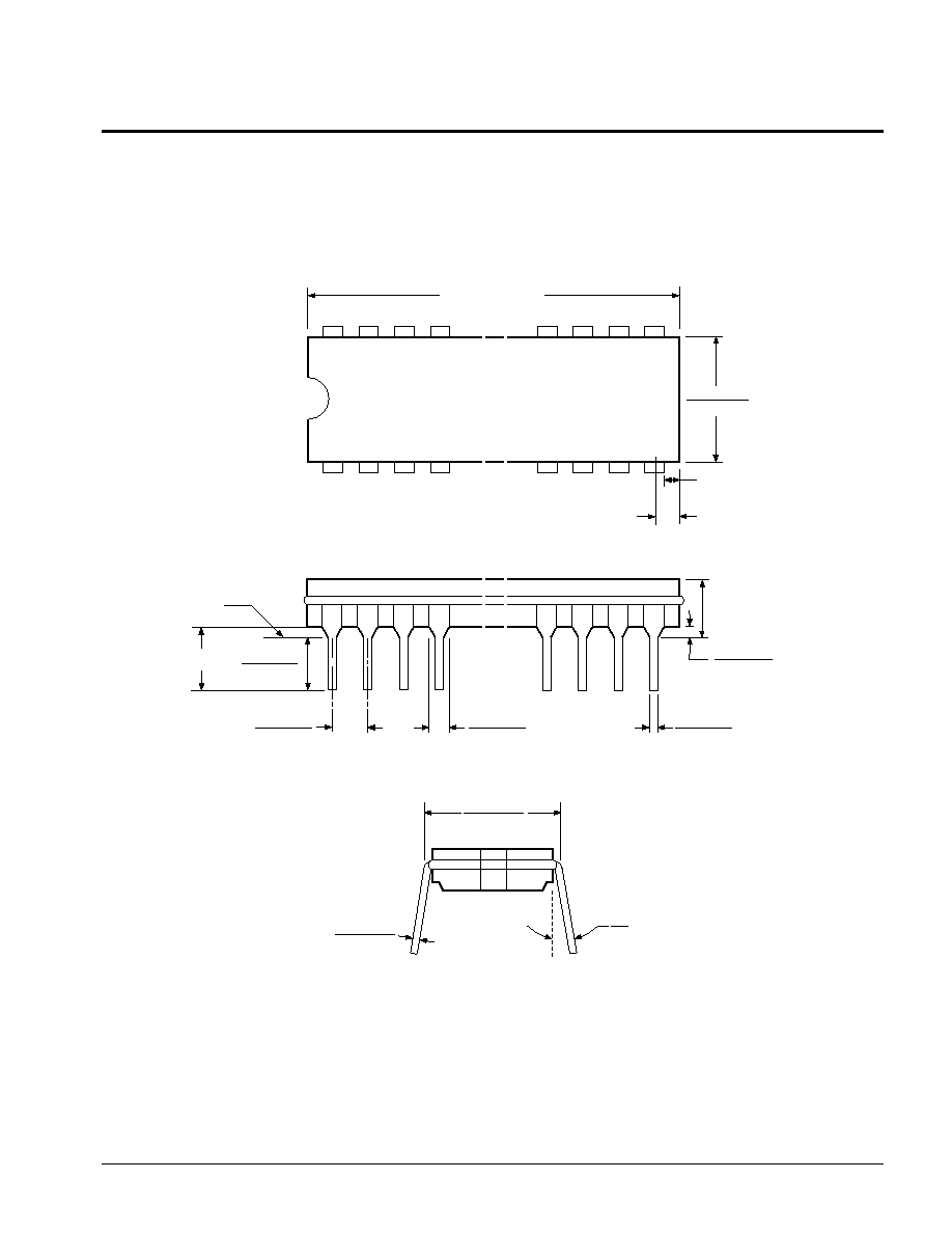
28-LEAD HERMETIC DUAL IN-LINE PACKAGE TYPE D
NOTE: ALL DIMENSIONS IN INCHES (IN PARENTHESES IN MILLIMETERS)
1.490 (37.85) MAX.
SEATING
PLANE
0.005 (0.127) MIN.
0.232 (5.90) MAX.
0.150 (3.81) MIN.
PACKAGING INFORMATION

X28VC256
18
0.021 (0.53)
0.013 (0.33)
0.420 (10.67)
0.050 (1.27) TYP.
TYP. 0.017 (0.43)
0.045 (1.14) x 45
∞
0.300 (7.62)
REF.
0.453 (11.51)
0.447 (11.35)
TYP. 0.450 (11.43)
0.495 (12.57)
0.485 (12.32)
TYP. 0.490 (12.45)
PIN 1
0.400
(10.16)
REF.
0.553 (14.05)
0.547 (13.89)
TYP. 0.550 (13.97)
0.595 (15.11)
0.585 (14.86)
TYP. 0.590 (14.99)
3
∞
TYP.
0.048 (1.22)
0.042 (1.07)
0.140 (3.56)
0.100 (2.45)
TYP. 0.136 (3.45)
0.095 (2.41)
0.060 (1.52)
--
0.015 (0.38)
SEATING PLANE
±
0.004 LEAD
CO ≠ PLANARITY
3926 Fhd F13
32-LEAD PLASTIC LEADED CHIP CARRIER PACKAGE TYPE J
NOTES:
1. ALL DIMENSIONS IN INCHES (IN PARENTHESES IN MILLIMETERS)
2. DIMENSIONS WITH NO TOLERANCE FOR REFERENCE ONLY
3926 FHD F13
PACKAGING INFORMATION
X28VC256
19
0.2980 (7.5692)
0.2920 (7.4168)
0.4160 (10.5664)
0.3980 (10.1092)
0.0192 (0.4877)
0.0138 (0.3505)
0.0160 (0.4064)
0.0100 (0.2540)
0.050 (1.270)
BSC
0.7080 (17.9832)
0.7020 (17.8308)
0.0110 (0.2794)
0.0040 (0.1016)
0.1040 (2.6416)
0.0940 (2.3876)
0.0350 (0.8890)
0.0160 (0.4064)
0.0125 (0.3175)
0.0090 (0.2311)
0
∞
≠ 8
∞
X 45
∞
3926 FHD F17
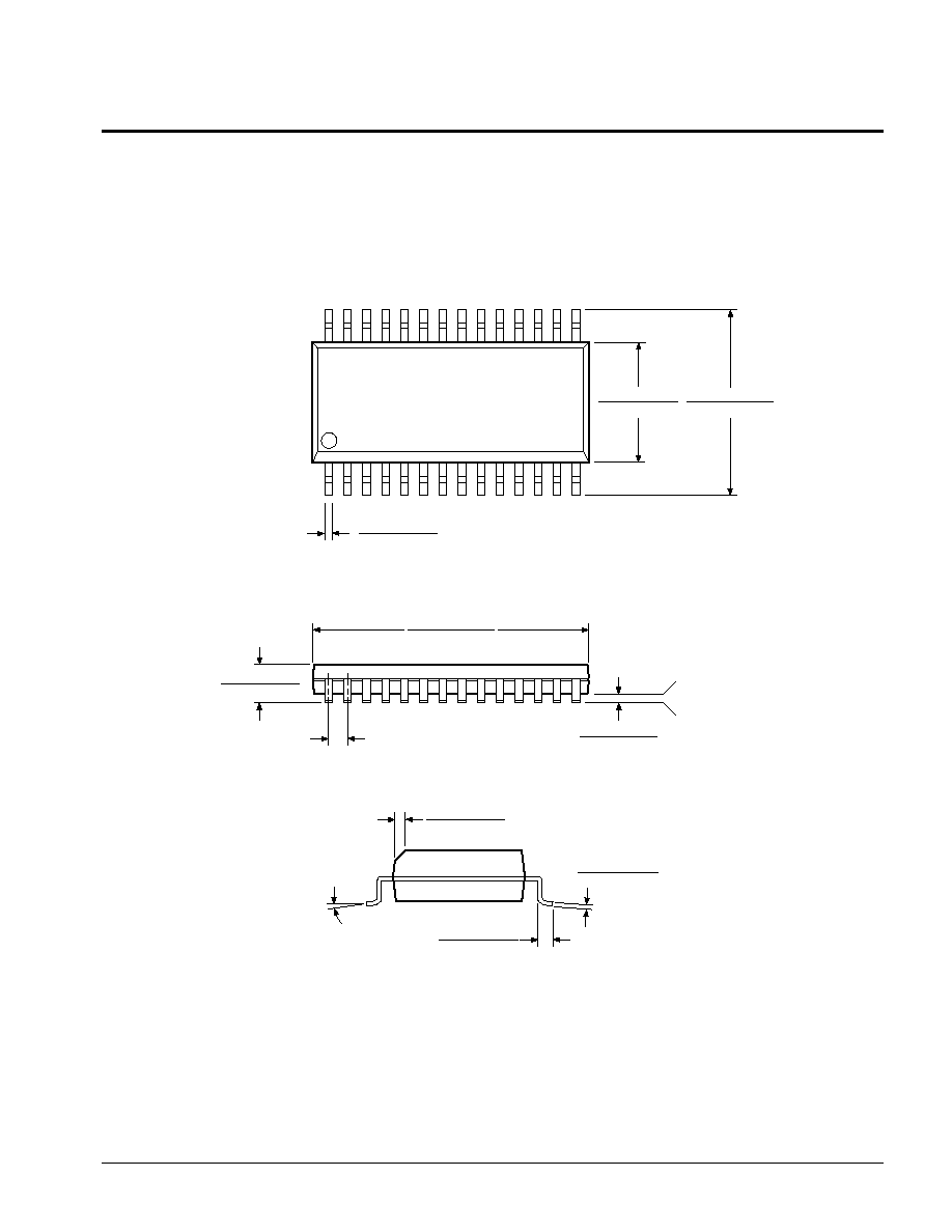
28-LEAD PLASTIC SMALL OUTLINE GULL WING PACKAGE TYPE S
NOTES:
1. ALL DIMENSIONS IN INCHES (IN PARENTHESES IN MILLIMETERS)
2. FORMED LEAD SHALL BE PLANAR WITH RESPECT TO ONE ANOTHER WITHIN 0.004 INCHES
3. BACK EJECTOR PIN MARKED "KOREA"
4. CONTROLLING DIMENSION: INCHES (MM)
SEATING PLANE
BASE PLANE
PACKAGING INFORMATION
X28VC256
20
0.150 (3.81) BSC
0.458 (11.63)
≠≠
0.458 (11.63)
0.442 (11.22)
PIN 1
3926 FHD F14
0.020 (0.51) x 45
∞
REF.
0.095 (2.41)
0.075 (1.91)
0.022 (0.56)
0.006 (0.15)
0.055 (1.39)
0.045 (1.14)
TYP. (4) PLCS.
0.040 (1.02) x 45
∞
REF.
TYP. (3) PLCS.
0.050 (1.27) BSC
0.028 (0.71)
0.022 (0.56)
(32) PLCS.
0.200 (5.08)
BSC
0.558 (14.17)
≠≠
0.088 (2.24)
0.050 (1.27)
0.120 (3.05)
0.060 (1.52)
PIN 1 INDEX CORNER
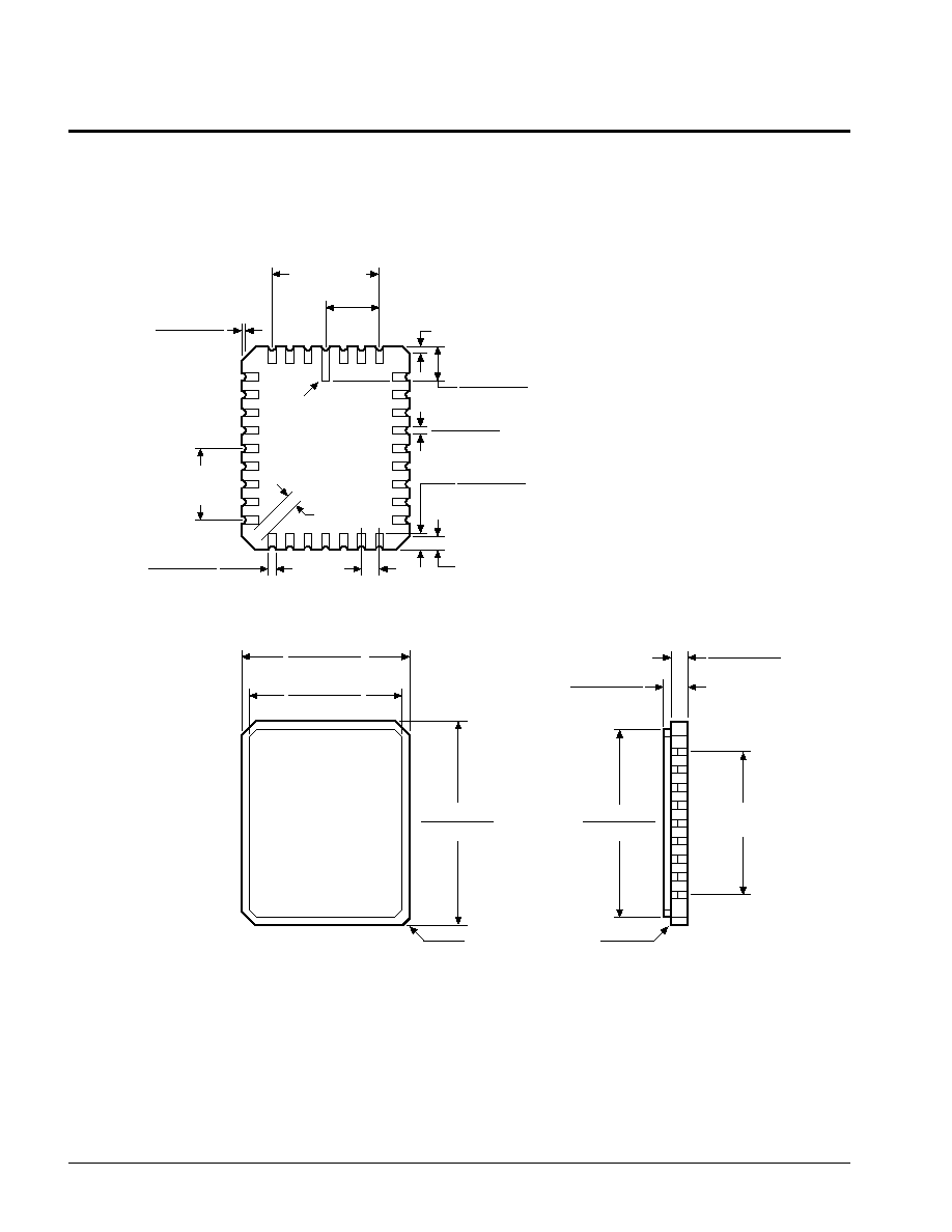
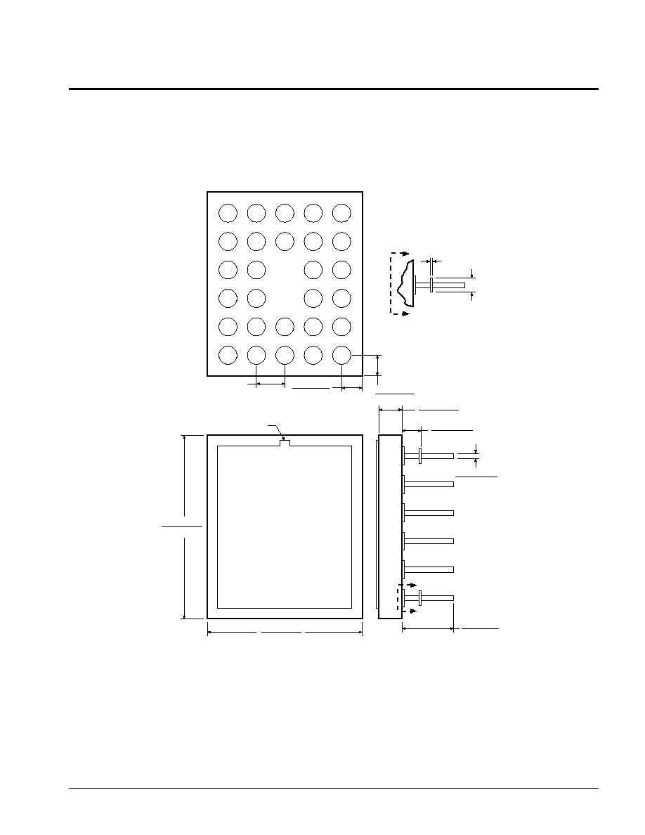
32-PAD CERAMIC LEADLESS CHIP CARRIER PACKAGE TYPE E
NOTE:
1. ALL DIMENSIONS IN INCHES (IN PARENTHESES IN MILLIMETERS)
2. TOLERANCE:
±
1% NLT
±
0.005 (0.127)
0.300 (7.62)
BSC
0.015 (0.38)
MIN.
0.400 (10.16)
BSC
0.560 (14.22)
0.540 (13.71)
DIA.
0.015 (0.38)
0.003 (0.08)
PACKAGING INFORMATION
X28VC256
21
0.561 (14.25)
0.541 (13.75)
3926 FHD F15
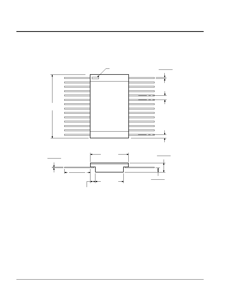
28-LEAD CERAMIC PIN GRID ARRAY PACKAGE TYPE K
NOTE: ALL DIMENSIONS IN INCHES (IN PARENTHESES IN MILLIMETERS)
0.020 (0.51)
0.016 (0.41)
12
13
15
17
18
11
10
14
16
19
9
8
20
21
7
6
22
23
5
2
28
24
25
4
3
1
27
26
TYP. 0.100 (2.54)
ALL LEADS
0.080 (2.03)
0.070 (1.78)
4 CORNERS
PIN 1 INDEX
0.660 (16.76)
0.640 (16.26)
0.110 (2.79)
0.080 (2.03)
0.072 (1.83)
0.061 (1.55)
0.185 (4.70)
0.175 (4.44)
0.050 (1.27)
0.008 (0.20)
A
A
A
A
NOTE: LEADS 4,12,18 & 26
0.080 (2.03)
0.070 (1.78)
PACKAGING INFORMATION
X28VC256
22
28-LEAD CERAMIC FLAT PACK TYPE F
3926 FHD F16
NOTE: ALL DIMENSIONS IN INCHES (IN PARENTHESES IN MILLIMETERS)
0.740 (18.80)
MAX.
0.019 (0.48)
0.015 (0.38)
0.050 (1.27) BSC
0.045 (1.14) MAX.
PIN 1 INDEX
1
28
0.130 (3.30)
0.090 (2.29)
0.045 (1.14)
0.025 (0.66)
0.180 (4.57)
MIN.
0.006 (0.15)
0.003 (0.08)
0.030 (0.76)
MIN.
0.370 (9.40)
0.250 (6.35)
TYP. 0.300 2 PLCS.
0.440 (11.18)
MAX.
PACKAGING INFORMATION
X28VC256
23
PACKAGING INFORMATION
3926 ILL F38.1
8.02 (0.315)
7.98 (0.314)
1.18 (0.046)
1.02 (0.040)
0.17 (0.007)
0.03 (0.001)
0.26 (0.010)
0.14 (0.006)
0.50 (0.0197) BSC
0.58 (0.023)
0.42 (0.017)
14.15 (0.557)
13.83 (0.544)
12.50 (0.492)
12.30 (0.484)
PIN #1 IDENT.
O 0.76 (0.03)
SEATING
PLANE
SEE NOTE 2
SEE NOTE 2
0.50 ± 0.04
(0.0197 ± 0.0016)
0.30 ± 0.05
(0.012 ± 0.002)
14.80 ± 0.05
(0.583 ± 0.002)
1.30 ± 0.05
(0.051 ± 0.002)
0.17 (0.007)
0.03 (0.001)
TYPICAL
32 PLACES
15 EQ. SPC. 0.50 ± 0.04
0.0197 ± 0.016 = 7.50 ± 0.06
(0.295 ± 0.0024) OVERALL
TOL. NON-CUMULATIVE
SOLDER PADS
FOOTPRINT
NOTE:
1. ALL DIMENSIONS ARE SHOWN IN MILLIMETERS (INCHES IN PARENTHESES).
32-LEAD THIN SMALL OUTLINE PACKAGE (TSOP) TYPE T

X28VC256
24
LIMITED WARRANTY
Devices sold by Xicor, Inc. are covered by the warranty and patent indemnification provisions appearing in its Terms of Sale only. Xicor, Inc. makes no warranty,
express, statutory, implied, or by description regarding the information set forth herein or regarding the freedom of the described devices from patent infringement.
Xicor, Inc. makes no warranty of merchantability or fitness for any purpose. Xicor, Inc. reserves the right to discontinue production and change specifications and
prices at any time and without notice.
Xicor, Inc. assumes no responsibility for the use of any circuitry other than circuitry embodied in a Xicor, Inc. product. No other circuits, patents, licenses are
implied.
U.S. PATENTS
Xicor products are covered by one or more of the following U.S. Patents: 4,263,664; 4,274,012; 4,300,212; 4,314,265; 4,326,134; 4,393,481; 4,404,475;
4,450,402; 4,486,769; 4,488,060; 4,520,461; 4,533,846; 4,599,706; 4,617,652; 4,668,932; 4,752,912; 4,829, 482; 4,874, 967; 4,883, 976. Foreign patents and
additional patents pending.
LIFE RELATED POLICY
In situations where semiconductor component failure may endanger life, system designers using this product should design the system with appropriate error
detection and correction, redundancy and back-up features to prevent such an occurrence.
Xicor's products are not authorized for use in critical components in life support devices or systems.
1. Life support devices or systems are devices or systems which, (a) are intended for surgical implant into the body, or (b) support or sustain life, and whose
failure to perform, when properly used in accordance with instructions for use provided in the labeling, can be reasonably expected to result in a significant
injury to the user.
2. A critical component is any component of a life support device or system whose failure to perform can be reasonably expected to cause the failure of the life
support device or system, or to affect its safety or effectiveness.
ORDERING INFORMATION
Device
Access Time
≠45 = 45ns
≠55 = 55ns
≠70 = 70ns
≠90 = 90ns
Temperature Range
Blank = Commercial = 0
∞
C to +70
∞
C
I = Industrial = ≠40
∞
C to +85
∞
C
M = Military = ≠55
∞
C to +125
∞
C
MB = MIL-STD-883
Package
P = 28-Lead Plastic DIP
D = 28-Lead Cerdip
J = 32-Lead PLCC
S = 28-Lead Plastic SOIC
E = 32-Pad LCC
K = 28-Lead Pin Grid Array
F = 28-Lead Flat Pack
T = 32-Lead TSOP
X28VC256 X X -X