
Characteristics subject to change without notice.
1 of 39
REV 1.0.4 7/12/01
www.xicor.com
X4023x
Integrated System Management IC
Triple Voltage Monitors, POR, 2 kbit EEPROM Memory, and Single/Dual DCP
DESCRIPTION
The X4023x family of Integrated System Management
ICs combine CPU Supervisor functions (V
CC
Power On
Reset (POR) circuitry, two additional programmable volt-
age monitor inputs with software and hardware indica-
tors), integrated EEPROM with Block Lock
TM
protection
and one or two Xicor Digitally Controlled Potentiometers
(XDCP). All functions of the X4023x are accessed by an
industry standard 2-Wire serial interface.
APPLICATIONS
The DCP of the X4023x may be utilized to software con-
trol analog voltages for:
≠ LCD contrast, LCD purity, or Backlight control.
≠ Power Supply settings such as PWM frequency, Voltage
Trimming or Margining (temperature offset control).
≠ Reference voltage setting (e.g. DDR-SDRAM SSTL-2)
The 2 kbit integrated EEPROM may be used to store ID,
manufacturer data, maintenance data and module defini-
tion data.
The programmable POR circuit insures V
CC
is stable
before RESET is removed and protects against brown-
outs and power failures. The programmable voltage mon-
itors have on-chip independent reference alarm levels.
With separate outputs, the voltage monitors can be used
for power on sequencing.
FEATURES
∑ Triple Voltage Monitors
--User Programmable Threshold Voltage
--Power On Reset (POR) Circuitry
--Software Selectable Reset timeout
--Manual Reset Input
∑ 2-Wire industry standard Serial Interface
∑ 2 kbit EEPROM with Write Protect & Block Lock
TM
∑ Digitally Controlled Potentiometers (DCP)
--Total Resistance
256 Tap = 100 k
,,,,
100 Tap or 64 Tap = 10 k
--Nonvolatile wiper position
--Write Protect Function
∑ Single Supply Operation
--2.7 V to 5.5 V
∑ 16 Pin SOIC (300) package
--SOIC
X4023X Family Selector Guide
X= 256 tap 100 tap 64 Tap
1
1
3
1
5
1
7
1
1
9
1
1
BLOCK DIAGRAM
DATA
REGISTER
COMMAND
DECODE &
CONTROL
LOGIC
SDA
SCL
POWER ON /
LOW VOLTAGE
CR
REGISTER
PROTECT LOGIC
EEPROM
THRESHOLD
RESET LOGIC
4
GENERATION
RESET
V2MON
V
CC
VTRIP
1
V3MON
+
-
2 kbit
RESET
Manual Reset (MR)
8
R
H
R
W
V2FAIL
WP
V3FAIL
ARRAY
2
©2000 Xicor Inc., Patents Pending (VTRIP
1,2,3
are user programmable)
WIPER
REGISTER
R
H
R
W
COUNTER
8 - BIT
NONVOLATILE
MEMORY
256 Tap DCP
Optional
64 or 100 Tap DCP
V
SS
VTRIP
2
VTRIP
3
WIPER
REGISTER
COUNTER
8 - BIT
NONVOLATILE
MEMORY
+
-
≠
+
Preliminary Information

X4023x
≠ Preliminary Information
Characteristics subject to change without notice.
2 of 39
REV 1.0.4 7/12/01
www.xicor.com
PIN CONFIGURATION
V2MON
V3MON
NC
3
4
V
CC
SDA
R
H0
R
W0
VSS
7
8
V3FAIL
NC
1
14
15
13
16
10
11
9
12
WP
6
NC
2
MR
5
SCL
RESET
V2FAIL
16 Pin SOIC
X40231
V2MON
V3MON
R
W1
3
4
V
CC
SDA
R
H1
NC
VSS
7
8
V3FAIL
NC
1
14
15
13
16
10
11
9
12
WP
6
NC
2
MR
5
SCL
RESET
V2FAIL
16 Pin SOIC
X40233
V2MON
V3MON
NC
3
4
V
CC
SDA
NC
NC
VSS
7
8
V3FAIL
R
H2
1
14
15
13
16
10
11
9
12
WP
6
R
W2
2
MR
5
SCL
RESET
V2FAIL
16 Pin SOIC
X40235
V2MON
V3MON
NC
3
4
V
CC
SDA
R
H0
R
W0
VSS
7
8
V3FAIL
R
H2
1
14
15
13
16
10
11
9
12
WP
6
R
W2
2
MR
5
SCL
RESET
V2FAIL
16 Pin SOIC
X40237
V2MON
V3MON
R
W1
3
4
V
CC
SDA
R
H1
NC
VSS
7
8
V3FAIL
R
H2
1
14
15
13
16
10
11
9
12
WP
6
R
W2
2
MR
5
SCL
RESET
V2FAIL
16 Pin SOIC
X40239
SINGLE XDCP
DUAL XDCP

X4023x
≠ Preliminary Information
Characteristics subject to change without notice.
3 of 39
REV 1.0.4 7/12/01
www.xicor.com
X40231 PIN ASSIGNMENT
SOIC
Name
Function
1
NC
No Connect
2
NC
No Connect
3
V3MON
V3MON Voltage Monitor Input.
V3MON i s the input to a non-inverting voltage comparator circuit. When the V3MON input is higher
than the V
TRIP3
threshold voltage, V3FAIL makes a transition to a HIGH level. Connect V3MON to V
SS
when not used.
4
V3FAIL
V3MON RESET Output.
This open drain output makes a transition to a HIGH level when V3MON is greater than V
TRIP3
and
goes LOW when V3MON is less than VTRIP3. There is no delay circuitry on this pin. The V3FAIL pin
requires the use of an external "pull-up" resistor.
5
MR
Manual Reset.
MR is a TTL level compatible input. Pulling the MR pin active (HIGH) initiates a reset cycle to the
RESET pin (V
CC
RESET Output pin). RESET will remain HIGH for time t
PURST
after MR has returned
to it's normally LOW state. The reset time can be selected using bits PUP1 and PUP0 in the CR
Register. The MR pin requires the use of an external "pull-down" resistor.
6
WP
Write Protect Control Pin.
WP pin is a TTL level compatible input. When held HIGH, Write Protection is enabled. In the enabled
state, this pin prevents all nonvolatile "write" operations. Also, when the Write Protection is enabled,
and the device Block Lock feature is active (i.e. the Block Lock bits are NOT [0,0]), then no "write"
(volatile or nonvolatile) operations can be performed in the device (including the wiper position of any
of the integrated Digitally Controlled Potentiometers (DCPs). The WP pin uses an internal "pull-down"
resistor, thus if left floating the write protection feature is disabled.
7
SCL
Serial Clock.
This is a TTL level compatible input pin used to control the serial bus timing for data input and output.
8
SDA
Serial Data.
SDA is a bidirectional TTL level compatible pin used to transfer data into and out of the device. The
SDA pin input buffer is always active (not gated). This pin requires an external pull up resistor.
9
VSS
Ground
.
10
NC
No Connect
11
R
H0
Connection to end of resistor array for (the 64 Tap) DCP.
12
R
W0
Connection to terminal equivalent to the "Wiper" of a mechanical potentiometer for DCP.
13
V2MON
V2MON Voltage Monitor Input.
V2MON is the input to a non-inverting voltage comparator circuit. When the V2MON input is greater
than the V
TRIP2
threshold voltage, V2FAIL makes a transition to a HIGH level. Connect V2MON to V
SS
when not used.
14
V2FAIL
V2MON RESET Output.
This open drain output makes a transition to a HIGH level when V2MON is greater than V
TRIP2
, and
goes LOW when V2MON is less than V
TRIP2
. There is no power up reset delay circuitry on this pin. The
V2FAIL pin requires the use of an external "pull-up" resistor.
15
RESET
V
CC
RESET Output.
This is an active HIGH, open drain output which becomes active whenever V
CC
falls below V
TRIP1
.
RESET becomes active on power up and remains active for a time t
PURST
after the power supply
stabilizes (t
PURST
can be changed by varying the PUP0 and PUP1 bits of the internal control register).
The RESET pin requires the use of an external "pull-up" resistor. The RESET pin can be forced active
(HIGH) using the manual reset (MR) input pin.
16
V
CC
Supply Voltage.

X4023x
≠ Preliminary Information
Characteristics subject to change without notice.
4 of 39
REV 1.0.4 7/12/01
www.xicor.com
X40233 PIN ASSIGNMENT
SOIC
Name
Function
1
NC
No Connect
2
NC
No Connect
3
V3MON
V3MON Voltage Monitor Input.
V3MON is the input to a non-inverting voltage comparator circuit. When the V3MON input is higher
than the V
TRIP3
threshold voltage, V3FAIL makes a transition to a HIGH level. Connect V3MON to V
SS
when not used.
4
V3FAIL
V3MON RESET Output.
This open drain output makes a transition to a HIGH level when V3MON is greater than V
TRIP3
and
goes LOW when V3MON is less than VTRIP3. There is no delay circuitry on this pin. The V3FAIL pin
requires the use of an external "pull-up" resistor.
5
MR
Manual Reset.
MR is a TTL level compatible input. Pulling the MR pin active (HIGH) initiates a reset cycle to the
RESET pin (V
CC
RESET Output pin). RESET will remain HIGH for time t
PURST
after MR has returned
to it's normally LOW state. The reset time can be selected using bits PUP1 and PUP0 in the CR
Register. The MR pin requires the use of an external "pull-down" resistor.
6
WP
Write Protect Control Pin.
WP pin is a TTL level compatible input. When held HIGH, Write Protection is enabled. In the enabled
state, this pin prevents all nonvolatile "write" operations. Also, when the Write Protection is enabled,
and the device Block Lock feature is active (i.e. the Block Lock bits are NOT [0,0]), then no "write"
(volatile or nonvolatile) operations can be performed in the device (including the wiper position of any
of the integrated Digitally Controlled Potentiometers (DCPs). The WP pin uses an internal "pull-down"
resistor, thus if left floating the write protection feature is disabled.
7
SCL
Serial Clock.
This is a TTL level compatible input pin used to control the serial bus timing for data input and output.
8
SDA
Serial Data.
SDA is a bidirectional TTL level compatible pin used to transfer data into and out of the device. The
SDA pin input buffer is always active (not gated). This pin requires an external pull up resistor.
9
VSS
Ground.
10
R
W1
Connection to terminal equivalent to the "Wiper" of a mechanical potentiometer for DCP.
11
R
H1
Connection to end of resistor array for (the 100 Tap) DCP.
12
NC
No Connect
13
V2MON
V2MON Voltage Monitor Input.
V2MON is the input to a non-inverting voltage comparator circuit. When the V2MON input is greater
than the V
TRIP2
threshold voltage, V2FAIL makes a transition to a HIGH level. Connect V2MON to V
SS
when not used.
14
V2FAIL
V2MON RESET Output.
This open drain output makes a transition to a HIGH level when V2MON is greater than V
TRIP2
, and
goes LOW when V2MON is less than V
TRIP2
. There is no power up reset delay circuitry on this pin.
The V2FAIL pin requires the use of an external "pull-up" resistor.
15
RESET
V
CC
RESET Output.
This is an active HIGH, open drain output which becomes active whenever V
CC
falls below V
TRIP1
.
RESET becomes active on power up and remains active for a time t
PURST
after the power supply
stabilizes (t
PURST
can be changed by varying the PUP0 and PUP1 bits of the internal control register).
The RESET pin requires the use of an external "pull-up" resistor. The RESET pin can be forced active
(HIGH) using the manual reset (MR) input pin.
16
V
CC
Supply Voltage.

X4023x
≠ Preliminary Information
Characteristics subject to change without notice.
5 of 39
REV 1.0.4 7/12/01
www.xicor.com
X40235 PIN ASSIGNMENT
SOIC
Name
Function
1
R
H2
Connection to end of resistor array for (the 256 Tap) DCP.
2
R
W2
Connection to terminal equivalent to the "Wiper" of a mechanical potentiometer for DCP.
3
V3MON
V3MON Voltage Monitor Input.
V3MON is the input to a non-inverting voltage comparator circuit. When the V3MON input is higher
than the V
TRIP3
threshold voltage, V3FAIL makes a transition to a HIGH level. Connect V3MON to V
SS
when not used.
4
V3FAIL
V3MON RESET Output.
This open drain output makes a transition to a HIGH level when V3MON is greater than V
TRIP3
and
goes LOW when V3MON is less than VTRIP3. There is no delay circuitry on this pin. The V3FAIL pin
requires the use of an external "pull-up" resistor.
5
MR
Manual Reset.
MR is a TTL level compatible input. Pulling the MR pin active (HIGH) initiates a reset cycle to the
RESET pin (V
CC
RESET Output pin). RESET will remain HIGH for time t
PURST
after MR has returned
to it's normally LOW state. The reset time can be selected using bits PUP1 and PUP0 in the CR
Register. The MR pin requires the use of an external "pull-down" resistor.
6
WP
Write Protect Control Pin.
WP pin is a TTL level compatible input. When held HIGH, Write Protection is enabled. In the enabled
state, this pin prevents all nonvolatile "write" operations. Also, when the Write Protection is enabled,
and the device Block Lock feature is active (i.e. the Block Lock bits are NOT [0,0]), then no "write"
(volatile or nonvolatile) operations can be performed in the device (including the wiper position of any
of the integrated Digitally Controlled Potentiometers (DCPs). The WP pin uses an internal "pull-down"
resistor, thus if left floating the write protection feature is disabled.
7
SCL
Serial Clock.
This is a TTL level compatible input pin used to control the serial bus timing for data input and output.
8
SDA
Serial Data.
SDA is a bidirectional TTL level compatible pin used to transfer data into and out of the device. The
SDA pin input buffer is always active (not gated). This pin requires an external pull up resistor.
9
VSS
Ground.
10
NC
No Connect
11
NC
No Connect
12
NC
No Connect
13
V2MON
V2MON Voltage Monitor Input.
V2MON is the input to a non-inverting voltage comparator circuit. When the V2MON input is greater
than the V
TRIP2
threshold voltage, V2FAIL makes a transition to a HIGH level. Connect V2MON to V
SS
when not used.
14
V2FAIL
V2MON RESET Output.
This open drain output makes a transition to a HIGH level when V2MON is greater than V
TRIP2
, and
goes LOW when V2MON is less than V
TRIP2
. There is no power up reset delay circuitry on this pin.
The V2FAIL pin requires the use of an external "pull-up" resistor.
15
RESET
V
CC
RESET Output.
This is an active HIGH, open drain output which becomes active whenever V
CC
falls below V
TRIP1
.
RESET becomes active on power up and remains active for a time t
PURST
after the power supply
stabilizes (t
PURST
can be changed by varying the PUP0 and PUP1 bits of the internal control register).
The RESET pin requires the use of an external "pull-up" resistor. The RESET pin can be forced active
(HIGH) using the manual reset (MR) input pin.
16
V
CC
Supply Voltage.

X4023x
≠ Preliminary Information
Characteristics subject to change without notice.
6 of 39
REV 1.0.4 7/12/01
www.xicor.com
X40237 PIN ASSIGNMENT
SOIC
Name
Function
1
R
H2
Connection to end of resistor array for (the 256 Tap) DCP2.
2
R
W2
Connection to terminal equivalent to the "Wiper" of a mechanical potentiometer for DCP2.
3
V3MON
V3MON Voltage Monitor Input.
V3MON is the input to a non-inverting voltage comparator circuit. When the V3MON input is higher
than the V
TRIP3
threshold voltage, V3FAIL makes a transition to a HIGH level. Connect V3MON to V
SS
when not used.
4
V3FAIL
V3MON RESET Output.
This open drain output makes a transition to a HIGH level when V3MON is greater than V
TRIP3
and
goes LOW when V3MON is less than VTRIP3. There is no delay circuitry on this pin. The V3FAIL pin
requires the use of an external "pull-up" resistor.
5
MR
Manual Reset. MR is a TTL level compatible input.
Pulling the MR pin active (HIGH) initiates a reset cycle to the RESET pin (V
CC
RESET Output pin).
RESET will remain HIGH for time t
PURST
after MR has returned to it's normally LOW state. The reset
time can be selected using bits PUP1 and PUP0 in the CR Register. The MR pin requires the use of
an external "pull-down" resistor.
6
WP
Write Protect Control Pin.
WP pin is a TTL level compatible input. When held HIGH, Write Protection is enabled. In the enabled
state, this pin prevents all nonvolatile "write" operations. Also, when the Write Protection is enabled,
and the device Block Lock feature is active (i.e. the Block Lock bits are NOT [0,0]), then no "write"
(volatile or nonvolatile) operations can be performed in the device (including the wiper position of any
of the integrated Digitally Controlled Potentiometers (DCPs). The WP pin uses an internal "pull-down"
resistor, thus if left floating the write protection feature is disabled.
7
SCL
Serial Clock.
This is a TTL level compatible input pin used to control the serial bus timing for data input and output.
8
SDA
Serial Data.
SDA is a bidirectional TTL level compatible pin used to transfer data into and out of the device. The
SDA pin input buffer is always active (not gated). This pin requires an external pull up resistor.
9
VSS
Ground.
10
NC
No Connect
11
R
H0
Connection to end of resistor array for (the 64 Tap) DCP0.
12
R
W0
Connection to terminal equivalent to the "Wiper" of a mechanical potentiometer for DCP0.
13
V2MON
V2MON Voltage Monitor Input.
V2MON is the input to a non-inverting voltage comparator circuit. When the V2MON input is greater
than the V
TRIP2
threshold voltage, V2FAIL makes a transition to a HIGH level. Connect V2MON to V
SS
when not used.
14
V2FAIL
V2MON RESET Output.
This open drain output makes a transition to a HIGH level when V2MON is greater than V
TRIP2
, and
goes LOW when V2MON is less than V
TRIP2
. There is no power up reset delay circuitry on this pin.
The V2FAIL pin requires the use of an external "pull-up" resistor.
15
RESET
V
CC
RESET Output.
This is an active HIGH, open drain output which becomes active whenever V
CC
falls below V
TRIP1
.
RESET becomes active on power up and remains active for a time t
PURST
after the power supply
stabilizes (t
PURST
can be changed by varying the PUP0 and PUP1 bits of the internal control register).
The RESET pin requires the use of an external "pull-up" resistor. The RESET pin can be forced active
(HIGH) using the manual reset (MR) input pin.
16
V
CC
Supply Voltage.

X4023x
≠ Preliminary Information
Characteristics subject to change without notice.
7 of 39
REV 1.0.4 7/12/01
www.xicor.com
X40239 PIN ASSIGNMENT
SOIC
Name
Function
1
R
H2
Connection to end of resistor array for (the 256 Tap) DCP2.
2
R
W2
Connection to terminal equivalent to the "Wiper" of a mechanical potentiometer for DCP2.
3
V3MON
V3MON Voltage Monitor Input.
V3MON is the input to a non-inverting voltage comparator circuit. When the V3MON input is higher
than the V
TRIP3
threshold voltage, V3FAIL makes a transition to a HIGH level. Connect V3MON to V
SS
when not used.
4
V3FAIL
V3MON RESET Output.
This open drain output makes a transition to a HIGH level when V3MON is greater than V
TRIP3
and
goes LOW when V3MON is less than V
TRIP3
. There is no delay circuitry on this pin. The V3FAIL pin
requires the use of an external "pull-up" resistor.
5
MR
Manual Reset. MR is a TTL level compatible input.
Pulling the MR pin active (HIGH) initiates a reset cycle to the RESET pin (V
CC
RESET Output pin).
RESET will remain HIGH for time t
PURST
after MR has returned to it's normally LOW state. The reset
time can be selected using bits PUP1 and PUP0 in the CR Register. The MR pin requires the use of
an external "pull-down" resistor.
6
WP
Write Protect Control Pin.
WP pin is a TTL level compatible input. When held HIGH, Write Protection is enabled. In the enabled
state, this pin prevents all nonvolatile "write" operations. Also, when the Write Protection is enabled,
and the device Block Lock feature is active (i.e. the Block Lock bits are NOT [0,0]), then no "write"
(volatile or nonvolatile) operations can be performed in the device (including the wiper position of any
of the integrated Digitally Controlled Potentiometers (DCPs). The WP pin uses an internal "pull-down"
resistor, thus if left floating the write protection feature is disabled.
7
SCL
Serial Clock.
This is a TTL level compatible input pin used to control the serial bus timing for data input and output.
8
SDA
Serial Data.
SDA is a bidirectional TTL level compatible pin used to transfer data into and out of the device. The
SDA pin input buffer is always active (not gated). This pin requires an external pull up resistor.
9
VSS
Ground.
10
R
W1
Connection to terminal equivalent to the "Wiper" of a mechanical potentiometer for DCP1
11
R
H1
Connection to end of resistor array for (the 100 Tap) DCP1.
12
NC
No Connect
13
V2MON
V2MON Voltage Monitor Input.
V2MON is the input to a non-inverting voltage comparator circuit. When the V2MON input is greater
than the V
TRIP2
threshold voltage, V2FAIL makes a transition to a HIGH level. Connect V2MON to V
SS
when not used.
14
V2FAIL
V2MON RESET Output.
This open drain output makes a transition to a HIGH level when V2MON is greater than V
TRIP2
, and
goes LOW when V2MON is less than V
TRIP2
. There is no power up reset delay circuitry on this pin.
The V2FAIL pin requires the use of an external "pull-up" resistor.
15
RESET
V
CC
RESET Output.
This is an active HIGH, open drain output which becomes active whenever V
CC
falls below V
TRIP1
.
RESET becomes active on power up and remains active for a time t
PURST
after the power supply
stabilizes (t
PURST
can be changed by varying the PUP0 and PUP1 bits of the internal control register).
The RESET pin requires the use of an external "pull-up" resistor. The RESET pin can be forced active
(HIGH) using the manual reset (MR) input pin.
16
V
CC
Supply Voltage.

X4023x
≠ Preliminary Information
Characteristics subject to change without notice.
8 of 39
REV 1.0.4 7/12/01
www.xicor.com
DETAILED DEVICE DESCRIPTION
The X4023x combines One or Two Xicor Digitally Con-
trolled Potentiometer (XDCP) devices, V
CC
power on
reset control, V
CC
low voltage reset control, two sup-
plementary voltage monitors with independent outputs,
and integrated EEPROM with Block LockTM protection,
in one package. The integrated functionality of the
X4023x lowers system cost, increases reliability, and
reduces board space requirements.
DCPs allow for the "set-and-forget" adjustment during
production test or in-system updating via the industry
standard 2-wire interface.
Applying voltage to V
CC
activates the Power On Reset
circuit which sets the RESET output HIGH, until the
supply voltage stabilizes for a period of time (50-300
msec selectable via software). The RESET output then
goes LOW. The Low Voltage Reset circuit sets the
RESET output HIGH when V
CC
falls below the mini-
mum V
CC
trip point. RESET remains HIGH until V
CC
returns to proper operating level and stabilizes for a
period of time (t
PURST)
. A Manual Reset (MR) input
allows the user to externally activate the RESET out-
put.
Two supplementary Voltage Monitor circuits, V2MON
and V3MON, continuously compare their inputs to indi-
vidual trip voltages (independent on-chip voltage refer-
ences factory set and user programmable). When an
input voltage exceeds it's associated trip level, the cor-
responding output (V3FAIL, V2FAIL) goes HIGH. When
the input voltage becomes lower than it's associated
trip level, the corresponding output is driven LOW. A
corresponding binary representation of the two monitor
circuit outputs (V2FAIL and V3FAIL) are also stored in
latched, volatile (CR) register bits. The status of these
two monitor outputs can be read out via the 2-wire
serial port. The bits will remain SET, even after the
alarm condition is removed, allowing advanced recov-
ery algorithms to be implemented.
Xicor's unique circuits allow for all internal trip voltages
to be individually programmed with high accuracy,
either by Xicor at final test or by the user during their
production process. Some distributors offer V
TRIP
reprogramming as a value added service. This gives
the designer great flexibility in changing system param-
eters, either at the time of manufacture, or in the field.
The memory portion of the device is a CMOS serial
EEPROM array with Xicor's Block Lock
TM
protection.
This memory may be used to store module manufac-
turing data, serial numbers, or various other system
parameters. The EEPROM array is internally organized
as x 8, and utilizes Xicor's proprietary Direct Write
TM
cells providing a minimum endurance of 1,000,000
cycles and a minimum data retention of 100 years.
The device features a 2-Wire interface.
PRINCIPLES OF OPERATION
SERIAL INTERFACE
Serial Interface Conventions
The device supports a bidirectional bus oriented proto-
col. The protocol defines any device that sends data
onto the bus as a transmitter, and the receiving device
as the receiver. The device controlling the transfer is
called the master and the device being controlled is
called the slave. The master always initiates data trans-
fers, and provides the clock for both transmit and
receive operations. The X4023x operates as a slave in
all applications.
Serial Clock and Data
Data states on the SDA line can change only while
SCL is LOW (see Figure 1). SDA state changes while
SCL is HIGH are reserved for indicating START and
STOP conditions. See Figure 1. On power up of the
X4023x, the SDA pin is in the input mode.
SCL
SDA
Data Stable
Data Change
Data Stable
Figure 1.
Valid Data Changes on the SDA Bus

X4023x
≠ Preliminary Information
Characteristics subject to change without notice.
9 of 39
REV 1.0.4 7/12/01
www.xicor.com
Serial Start Condition
All commands are preceded by the START condition,
which is a HIGH to LOW transition of SDA while SCL is
HIGH. The device continuously monitors the SDA and
SCL lines for the START condition and does not
respond to any command until this condition has been
met. See Figure 2.
Serial Stop Condition
All communications must be terminated by a STOP
condition, which is a LOW to HIGH transition of SDA
while SCL is HIGH. The STOP condition is also used to
place the device into the Standby power mode after a
read sequence. A STOP condition can only be issued
after the transmitting device has released the bus. See
Figure 2.
Serial Acknowledge
An ACKNOWLEDGE (ACK) is a software convention
used to indicate a successful data transfer. The trans-
mitting device, either master or slave, will release the
bus after transmitting eight bits. During the ninth clock
cycle, the receiver will pull the SDA line LOW to
ACKNOWLEDGE that it received the eight bits of data.
Refer to Figure 3
The device will respond with an ACKNOWLEDGE after
recognition of a START condition if the correct Device
Identifier bits are contained in the Slave Address Byte.
If a write operation is selected, the device will respond
with an ACKNOWLEDGE after the receipt of each sub-
sequent eight bit word.
In the read mode, the device will transmit eight bits of
data, release the SDA line, then monitor the line for an
ACKNOWLEDGE. If an ACKNOWLEDGE is detected
and no STOP condition is generated by the master, the
device will continue to transmit data. The device will ter-
minate further data transmissions if an ACKNOWL-
EDGE is not detected. The master must then issue a
STOP condition to place the device into a known state.
DEVICE INTERNAL ADDRESSING
Addressing Protocol Overview
The user addressable internal components of the
X4023x can be split up into three main parts:
Data Output from
Transmitter
Data Output
from Receiver
8
1
9
Start
Acknowledge
Figure 3.
Acknowledge Response From Receiver
SCL from
Master
SCL
SDA
Start
Stop
Figure 2.
Valid Start and Stop Conditions

X4023x
≠ Preliminary Information
Characteristics subject to change without notice.
10 of 39
REV 1.0.4 7/12/01
www.xicor.com
--One or Two Digitally Controlled Potentiometers (DCPs)
--EEPROM array
--Control and Status (CR) Register
Depending upon the operation to be performed on
each of these individual parts, a 1, 2 or 3 Byte protocol
is used. All operations however must begin with the
Slave Address Byte being issued on the SDA pin. The
Slave address selects the part of the X4023x to be
addressed, and specifies if a Read or Write operation is
to be performed.
It should be noted that in order to perform a write oper-
ation to either a DCP or the EEPROM array, the Write
Enable Latch (WEL) bit must first be set (See "BL1,
BL0: Block Lock protection bits - (Nonvolatile)" on
page 18.)
Slave Address Byte
Following a START condition, the master must output a
Slave Address Byte (Refer to Figure 4). This byte con-
sists of three parts:
--The Device Type Identifier which consists of the most
significant four bits of the Slave Address (SA7 - SA4).
The Device Type Identifier must always be set to 1010
in order to select the X4023x.
--The next three bits (SA3 - SA1) are the Internal Device
Address bits. Setting these bits to 000 internally selects
the EEPROM array, while setting these bits to 111
selects the DCP structures in the X4023x. The CR Reg-
ister may be selected using the Internal Device Address
010.
--The Least Significant Bit of the Slave Address (SA0)
Byte is the R/W bit. This bit defines the operation to be
performed on the device being addressed (as defined
in the bits SA3 - SA1). When the R/W bit is "1", then a
READ operation is selected. A "0" selects a WRITE
operation (Refer to Figure 4)
Nonvolatile Write Acknowledge Polling
After a nonvolatile write command sequence (for either
the EEPROM array, the Non Volatile Memory of a DCP
(NVM), or the CR Register) has been correctly issued
(including the final STOP condition), the X4023x ini-
tiates an internal high voltage write cycle. This cycle
typically requires 5 ms. During this time, no further
Read or Write commands can be issued to the device.
Write Acknowledge Polling is used to determine when
this high voltage write cycle has been completed.
To perform acknowledge polling, the master issues a
START condition followed by a Slave Address Byte.
The Slave Address issued must contain a valid Internal
Device Address. The LSB of the Slave Address (R/W)
can be set to either 1 or 0 in this case. If the device is
still busy with the high voltage cycle then no
ACKNOWLEDGE will be returned. If the device has
completed the write operation, an ACKNOWLEDGE
will be returned and the host can then proceed with a
read or write operation. (Refer to Figure 5)
DIGITALLY CONTROLLED POTENTIOMETERS
DCP Functionality
The X4023x includes one or two independent resistor
arrays. For the 64, 100 or 256 tap XDCPs, these arrays
respectively contain 63, 99 discrete resistive segments
that are connected in series. (the 256 tap resistor
achieves an equivalent end to end resistance.) The
physical ends of each array are equivalent to the fixed
terminals of a mechanical potentiometer. At one end of
the resistor array the terminal connects to the R
Hx
pin
(x = 0,1,2).The other end of the resistor array is con-
nected to V
SS
inside the package.
SA6
SA7
SA5
SA3
SA2
SA1
SA0
DEVICE TYPE
IDENTIFIER
READ /
SA4
Internal Address
(SA3 - SA1)
Internally Addressed
Device
000
EEPROM Array
010
CR Register
111
DCP
Bit SA0
Operation
0
WRITE
1
READ
R/W
Figure 4.
Slave Address Format
1 0 1
0
WRITE
ADDRESS
INTERNAL
DEVICE

X4023x
≠ Preliminary Information
Characteristics subject to change without notice.
11 of 39
REV 1.0.4 7/12/01
www.xicor.com
At both ends of each array and between each resistor
segment there is a CMOS switch connected between
the resistor array and the wiper (R
w
x
) output. Within
each individual array, only one switch may be turned on
at any one time. These switches are controlled by the
Wiper Counter Register (WCR) (See Figure 6). The
WCR is a volatile register.
On power up of the X4023x, wiper position data is auto-
matically loaded into the WCR from its associated Non
Volatile Memory (NVM) Register. The Table below
shows the Initial Values of the DCP WCR's before the
contents of the NVM is loaded into the WCR.
The data in the WCR is then decoded to select and
enable one of the respective FET switches. A "make
before break" sequence is used internally for the FET
switches when the wiper is moved from one tap posi-
tion to another.
Hot Pluggability
Figure 7 shows a typical waveform that the X4023x
might experience in a Hot Pluggable situation. On
power up, V
CC
applied to the X4023x may exhibit some
amount of ringing, before it settles to the required
value.
The device is designed such that the wiper terminal
(R
Wx
) is recalled to the correct position (as per the last
stored in the DCP NVM), when the voltage applied to
V
CC
exceeds V
TRIP1
for a time exceeding t
PURST
(the
Power On Reset time, set in the CR Register - See
"CONTROL AND STATUS REGISTER" on page 18.).
Therefore, if
t
trans
is defined as the time taken for V
CC
to settle above V
TRIP1
(Figure 7): then the desired
wiper terminal position is recalled by (a maximum)
time:
t
trans
+
t
PURST
. It should be noted that
t
trans
is
determined by system hot plug conditions.
DCP Operations
In total there are three operations that can be per-
formed on any internal DCP structure:
--DCP Nonvolatile Write
--DCP Volatile Write
--DCP Read
ACK
returned?
Issue Slave Address
Byte (Read or Write)
Byte load completed
by issuing STOP.
Enter ACK Polling
Issue STOP
Issue START
NO
YES
High Voltage Cycle
complete. Continue
command sequence?
Issue STOP
NO
Continue normal
Read or Write
command sequence
PROCEED
YES
Figure 5.
Acknowledge Polling Sequence
DECODER
RESISTOR
ARRAY
R
Hx
FET
SWITCHES
R
Wx
0
1
2
N
WIPER
REGISTER
COUNTER
NON
MEMORY
VOLATILE
(WCR)
(NVM)
"WIPER"
Figure 6.
DCP Internal Structure
DCP
Initial Values Before Recall
R
0
(64 TAP)
V
H
(TAP = 63)
R
1
(100 TAP)
V
L
(TAP = 0)
R
2
(256 TAP)
V
H
(TAP = 255)

X4023x
≠ Preliminary Information
Characteristics subject to change without notice.
12 of 39
REV 1.0.4 7/12/01
www.xicor.com
A nonvolatile write to a DCP will change the "wiper
position" by simultaneously writing new data to the
associated WCR and NVM. Therefore, the new "wiper
position" setting is recalled into the WCR after V
CC
of
the X4023x is powered down and then powered back
up.
A volatile write operation to a DCP however, changes
the "wiper position" by writing new data to the associ-
ated WCR only. The contents of the associated NVM
register remains unchanged. Therefore, when V
CC
to
the device is powered down then back up, the "wiper
position" reverts to that last position written to the DCP
using a nonvolatile write operation.
Both volatile and nonvolatile write operations are exe-
cuted using a three byte command sequence: (DCP)
Slave Address Byte, Instruction Byte, followed by a
Data Byte (See Figure 9)
A DCP Read operation allows the user to "read out" the
current "wiper position" of the DCP, as stored in the
associated WCR. This operation is executed using the
Random Address Read command sequence, consist-
ing of the (DCP) Slave Address Byte followed by an
Instruction Byte and the Slave Address Byte again
(Refer to Figure 10).
Instruction Byte
While the Slave Address Byte is used to select the
DCP devices, an Instruction Byte is used to determine
which DCP is being addressed.
The Instruction Byte (Figure 8) is valid only when the
Device Type Identifier and the Internal Device Address
bits of the Slave Address are set to 1010111. In this
case, the two Least Significant Bit's (I1 - I0) of the
Instruction Byte are used to select the particular DCP
(0 - 2). In the case of a Write to any of the DCPs (i.e.
the LSB of the Slave Address is 0), the Most Significant
Bit of the Instruction Byte (I7), determines the Write
Type (WT) performed.
If WT is "1", then a Nonvolatile Write to the DCP
occurs.
In this case, the "wiper position" of the DCP is changed
by simultaneously writing new data to the associated
WCR and NVM. Therefore, the new "wiper position"
setting is recalled into the WCR after V
CC
of the
X4023x has been powered down then powered back
up
If WT is "0" then a DCP Volatile Write is performed. This
operation changes the DCP "wiper position" by writing
new data to the associated WCR only. The contents of
Figure 7.
DCP Power up
t
V
CC
V
TRIP1
V
CC (Max.)
t
PURST
Maximum Wiper Recall time
0
t
TRANS
WT
Description
0
Select a Volatile Write operation to be performed
on the DCP pointed to by bits P1 and P0
1
Select a Nonvolatile Write operation to be per-
formed on the DCP pointed to by bits P1 and P0
0
0
WT
0
0
0
P1
P0
WRITE TYPE
DCP SELECT
This bit has no effect when a Read operation is being performed.
I5
I6
I7
I4
I3
I2
I1
I0
Figure 8.
Instruction Byte Format

X4023x
≠ Preliminary Information
Characteristics subject to change without notice.
13 of 39
REV 1.0.4 7/12/01
www.xicor.com
the associated NVM register remains unchanged.
Therefore, when V
CC
to the device is powered down
then back up, the "wiper position" reverts to that last
written to the DCP using a nonvolatile write operation.
DCP Write Operation
A write to DCPx (x=0,1,2) can be performed using the
three byte command sequence shown in Figure 9.
In order to perform a write operation on a particular
DCP, the Write Enable Latch (WEL) bit of the CR Reg-
ister must first be set (See "BL1, BL0: Block Lock pro-
tection bits - (Nonvolatile)" on page 18.)
The Slave Address Byte 10101110 specifies that a
Write to a DCP is to be conducted. An ACKNOWL-
EDGE is returned by the X4023x after the Slave
Address, if it has been received correctly.
Next, an Instruction Byte is issued on SDA. Bits P1 and
P0 of the Instruction Byte determine which WCR is to
be written, while the WT bit determines if the Write is to
be volatile or nonvolatile. If the Instruction Byte format
is valid, another ACKNOWLEDGE is then returned by
the X4023x.
Following the Instruction Byte, a Data Byte is issued to
the X4023x over SDA. The Data Byte contents is
latched into the WCR of the DCP on the first rising
edge of the clock signal, after the LSB of the Data Byte
(D0) has been issued on SDA (See Figure 34).
The Data Byte determines the "wiper position" (which
FET switch of the DCP resistive array is switched ON)
of the DCP. The maximum value for the Data Byte
depends upon which DCP is being addressed (see fol-
lowing table).
Using a Data Byte larger than the values specified
above results in the "wiper terminal" being set to the
highest tap position. The "wiper position" does NOT
roll-over to the lowest tap position.
For DCP0 (64 Tap) and DCP2 (256 Tap), the Data Byte
maps one to one to the "wiper position" of the DCP
"wiper terminal". Therefore, the Data Byte 00001111
(15
10
) corresponds to setting the "wiper terminal" to
tap position 15. Similarly, the Data Byte 00011100
(28
10
) corresponds to setting the "wiper terminal" to
tap position 28. The mapping of the Data Byte to "wiper
position" data for DCP1 (100 Tap), is shown in
"APPENDIX 1" . An example of a simple C language
function which "translates" between the tap position
(decimal) and the Data Byte (binary) for DCP1, is given
in "APPENDIX 2" .
It should be noted that all writes to any DCP of the
X4023x are random in nature. Therefore, the Data Byte
of consecutive write operations to any DCP can differ
by an arbitrary number of bits. Also, setting the bits
P1=1, P0=1 is a reserved sequence, and will result in
no ACKNOWLEDGE after sending an Instruction Byte
on SDA.
The factory default setting of all "wiper position" set-
tings is with 00h stored in the NVM of the DCPs. This
corresponds to having the "wiper terminal"
R
WX
(x=0,1,2) at the "lowest" tap position, Therefore, the
resistance between
R
WX
and
R
LX
is a minimum
(essentially only the Wiper Resistance,
R
W
).
S
T
A
R
T
1
0
1
0
1
1
1
0
A
C
K
WT
0
0
0
0
0
P1 P0
A
C
K
S
T
O
P
A
C
K
D7
D6
D5
D4
D3
D2
D1
D0
SLAVE ADDRESS BYTE
INSTRUCTION BYTE
DATA BYTE
Figure 9.
DCP Write Command Sequence
P1- P0
DCPx
# Taps
Max. Data Byte
0
0
x=0
64
3Fh
0
1
x=1
100
Refer to Appendix 1
1
0
x=2
256
FFh
1
1
Reserved

X4023x
≠ Preliminary Information
Characteristics subject to change without notice.
14 of 39
REV 1.0.4 7/12/01
www.xicor.com
DCP Read Operation
A read of DCPx (x=0,1,2) can be performed using the
three byte random read command sequence shown in
Figure 10.
The master issues the START condition and the Slave
Address Byte 10101110 which specifies that a
"dummy" write" is to be conducted. This "dummy" write
operation sets which DCP is to be read (in the preced-
ing Read operation). An ACKNOWLEDGE is returned
by the X4023x after the Slave Address if received cor-
rectly. Next, an Instruction Byte is issued on SDA. Bits
P1-P0 of the Instruction Byte determine which DCP
"wiper position" is to be read. In this case, the state of
the WT bit is "don't care". If the Instruction Byte format
is valid, then another ACKNOWLEDGE is returned by
the X4023x.
Following this ACKNOWLEDGE, the master immedi-
ately issues another START condition and a valid Slave
address byte with the R/W bit set to 1. Then the
X4023x issues an ACKNOWLEDGE followed by Data
Byte, and finally, the master issues a STOP condition.
The Data Byte read in this operation, corresponds to
the "wiper position" (value of the WCR) of the DCP
pointed to by bits P1 and P0.
It should be noted that when reading out the data byte
for DCP0 (64 Tap), the upper two most significant bits
are "unknown" bits. For DCP1 (100 Tap), the upper
most significant bit is an "unknown". For DCP2 (256
Tap) however, all bits of the data byte are relevant (See
Figure 10).
Slave
Address
Instruction
Byte
A
C
K
A
C
K
S
t
a
r
t
S
t
o
p
Slave
Address
Data Byte
A
C
K
S
t
a
r
t
SDA Bus
Signals from
the Slave
Signals from
the Master
Figure 10. DCP Read Sequence
"Dummy" write
READ Operation
1 0 1
1 1 1 0
0
0 0
0 0
0
W
T
P
1
P
0
1 0 1
1 1 1 1
0
WRITE Operation
-
- -
MSB
LSB
DCPx
x = 0
x = 1
x = 2
"-" = DON'T CARE
S
t
a
r
t
S
t
o
p
Slave
Address
Address
Byte
Data
Byte
A
C
K
A
C
K
A
C
K
SDA Bus
Signals from
the Slave
Signals from
the Master
Figure 11. EEPROM Byte Write Sequence
Internal
Device
Address
1 0 1 0 0 0 0 0
WRITE Operation

X4023x
≠ Preliminary Information
Characteristics subject to change without notice.
15 of 39
REV 1.0.4 7/12/01
www.xicor.com
2 kbit EEPROM ARRAY
Operations on the 2 kbit EEPROM Array, consist of
either 1, 2 or 3 byte command sequences. All opera-
tions on the EEPROM must begin with the Device Type
Identifier of the Slave Address set to 1010000. A Read
or Write to the EEPROM is selected by setting the LSB
of the Slave Address to the appropriate value R/W
(Read = "1", Write="0").
In some cases when performing a Read or Write to the
EEPROM, an Address Byte may also need to be speci-
fied. This Address Byte can contain the values 00h to
FFh.
EEPROM Byte Write
In order to perform an EEPROM Byte Write operation
to the EEPROM array, the Write Enable Latch (WEL)
bit of the CR Register must first be set (See "BL1, BL0:
Block Lock protection bits - (Nonvolatile)" on page 18.)
For a write operation, the X4023x requires the Slave
Address Byte and an Address Byte. This gives the
master access to any one of the words in the array.
After receipt of the Address Byte, the X4023x responds
with an ACKNOWLEDGE, and awaits the next eight
bits of data. After receiving the 8 bits of the Data Byte,
it again responds with an ACKNOWLEDGE. The mas-
ter then terminates the transfer by generating a STOP
condition, at which time the X4023x begins the internal
write cycle to the nonvolatile memory (See Figure 11).
During this internal write cycle, the X4023x inputs are
disabled, so it does not respond to any requests from
the master. The SDA output is at high impedance. A
write to a region of EEPROM memory which has been
protected with the Block-Lock feature (See "BL1, BL0:
Block Lock protection bits - (Nonvolatile)" on page 18.),
suppresses the ACKNOWLEDGE bit after the Address
Byte.
EEPROM Page Write
In order to perform an EEPROM Page Write operation
to the EEPROM array, the Write Enable Latch (WEL)
bit of the CR Register must first be set (See "BL1, BL0:
Block Lock protection bits - (Nonvolatile)" on page 18.)
The X4023x is capable of a page write operation. It is
initiated in the same manner as the byte write opera-
tion; but instead of terminating the write cycle after the
first data byte is transferred, the master can transmit an
unlimited number of 8-bit bytes. After the receipt of
each byte, the X4023x responds with an ACKNOWL-
EDGE, and the address is internally incremented by
one. The page address remains constant. When the
counter reaches the end of the page, it "rolls over" and
goes back to `0' on the same page.
For example, if the master writes 12 bytes to the page
starting at location 11 (decimal), the first 5 bytes are
written to locations 11 through 15, while the last 7 bytes
are written to locations 0 through 6. Afterwards, the
address counter would point to location 7. If the master
supplies more than 16 bytes of data, then new data
overwrites the previous data, one byte at a time (See
Figure 13).
The master terminates the Data Byte loading by issu-
ing a STOP condition, which causes the X4023x to
begin the nonvolatile write cycle. As with the byte write
operation, all inputs are disabled until completion of the
internal write cycle. See Figure 12 for the address,
ACKNOWLEDGE, and data transfer sequence.
S
t
a
r
t
S
t
o
p
Slave
Address
Address
Byte
Data
(n)
A
C
K
A
C
K
A
C
K
SDA Bus
Signals from
the Slave
Signals from
the Master
Data
(1)
A
C
K
(2 < n < 16)
Figure 12. EEPROM Page Write Operation
1 0 1 0 0 0 0 0

X4023x
≠ Preliminary Information
Characteristics subject to change without notice.
16 of 39
REV 1.0.4 7/12/01
www.xicor.com
Stops and EEPROM Write Modes
Stop conditions that terminate write operations must be
sent by the master after sending at least 1 full data byte
and receiving the subsequent ACKNOWLEDGE signal.
If the master issues a STOP within a Data Byte, or
before the X4023x issues a corresponding ACKNOWL-
EDGE, the X4023x cancels the write operation. There-
fore, the contents of the EEPROM array does not
change.
EEPROM Array Read Operations
Read operations are initiated in the same manner as
write operations with the exception that the R/W bit of
the Slave Address Byte is set to one. There are three
basic read operations: Current EEPROM Address
Read, Random EEPROM Read, and Sequential
EEPROM Read.
Current EEPROM Address Read
Internally the device contains an address counter that
maintains the address of the last word read incre-
mented by one. Therefore, if the last read was to
address n, the next read operation would access data
from address n+1. On power up, the address of the
address counter is undefined, requiring a read or write
operation for initialization.
Upon receipt of the Slave Address Byte with the R/W
bit set to one, the device issues an ACKNOWLEDGE
and then transmits the eight bits of the Data Byte. The
master terminates the read operation when it does not
respond with an ACKNOWLEDGE during the ninth
clock and then issues a STOP condition (See Figure 14
for the address, ACKNOWLEDGE, and data transfer
sequence).
It should be noted that the ninth clock cycle of the read
operation is not a "don't care." To terminate a read
operation, the master must either issue a STOP condi-
tion during the ninth cycle or hold SDA HIGH during the
ninth clock cycle and then issue a STOP condition.
Another important point to note regarding the "Current
EEPROM Address Read" , is that this operation is not
available if the last executed operation was an access
to a DCP or the CR Register (i.e.: an operation using
address
address
11
5 bytes
15
7 bytes
address
= 6
address pointer
ends here
Addr = 7
Figure 13. Example: Writing 12 bytes to a 16-byte page starting at location 11.
5 bytes
10
10
10
10
S
t
a
r
t
S
t
o
p
Slave
Address
Data
A
C
K
SDA Bus
Signals from
the Slave
Signals from
the Master
Figure 14. Current EEPROM Address Read Sequence
1 0 1 0 0 0 0 1

X4023x
≠ Preliminary Information
Characteristics subject to change without notice.
17 of 39
REV 1.0.4 7/12/01
www.xicor.com
the Device Type Identifier 1010111 or 1010010). Imme-
diately after an operation to a DCP or CR Register is
performed, only a "Random EEPROM Read" is avail-
able. Immediately following a "Random EEPROM
Read" , a "Current EEPROM Address Read" or
"Sequential EEPROM Read" is once again available
(assuming that no access to a DCP or CR Register
occur in the interim).
Random EEPROM Read
Random read operation allows the master to access
any memory location in the array. Prior to issuing the
Slave Address Byte with the R/W bit set to one, the
master must first perform a "dummy" write operation.
The master issues the START condition and the Slave
Address Byte, receives an ACKNOWLEDGE, then
issues an Address Byte. This "dummy" Write operation
sets the address pointer to the address from which to
begin the random EEPROM read operation.
After the X4023x acknowledges the receipt of the
Address Byte, the master immediately issues another
START condition and the Slave Address Byte with the
R/W bit set to one. This is followed by an ACKNOWL-
EDGE from the X4023x and then by the eight bit word.
The master terminates the read operation by not
responding with an ACKNOWLEDGE and instead issu-
ing a STOP condition (Refer to Figure 15).
A similar operation called "Set Current Address" also
exists. This operation is performed if a STOP is issued
instead of the second START shown in Figure 15. In
this case, the device sets the address pointer to that of
the Address Byte, and then goes into standby mode
after the STOP bit. All bus activity will be ignored until
another START is detected.
Slave
Address
Address Byte
A
C
K
A
C
K
S
t
a
r
t
S
t
o
p
Slave
Address
Data
A
C
K
S
t
a
r
t
SDA Bus
Signals from
the Slave
Signals from
the Master
Figure 15. Random EEPROM Address Read Sequence
0 1 0 0 0 0
1
1 0 1 0 0 0 0
WRITE Operation
"Dummy" Write
READ Operation
0
1
Data
(2)
S
t
o
p
Slave
Address
Data
(n)
A
C
K
A
C
K
SDA Bus
Signals from
the Slave
Signals from
the Master
1
Data
(n-1)
A
C
K
A
C
K
(n is any integer greater than 1)
Data
(1)
Figure 16. Sequential EEPROM Read Sequence
0 0 0

X4023x
≠ Preliminary Information
Characteristics subject to change without notice.
18 of 39
REV 1.0.4 7/12/01
www.xicor.com
Sequential EEPROM Read
Sequential reads can be initiated as either a current
address read or random address read. The first Data
Byte is transmitted as with the other modes; however,
the master now responds with an ACKNOWLEDGE,
indicating it requires additional data. The X4023x con-
tinues to output a Data Byte for each ACKNOWLEDGE
received. The master terminates the read operation by
not responding with an ACKNOWLEDGE and instead
issuing a STOP condition.
The data output is sequential, with the data from
address n followed by the data from address n + 1. The
address counter for read operations increments
through the entire memory contents to be serially read
during one operation. At the end of the address space
the counter "rolls over" to address 00h and the device
continues to output data for each ACKNOWLEDGE
received (Refer to Figure 16).
CONTROL AND STATUS REGISTER
The Control and Status (CR) Register provides the
user with a mechanism for changing and reading the
status of various parameters of the X4023x (See Fig-
ure 17).
The CR register is a combination of both volatile and
nonvolatile bits. The nonvolatile bits of the CR register
retain their stored values even when V
CC
is powered
down, then powered back up. The volatile bits however,
will always power up to a known logic state "0" (irre-
spective of their value at power down).
A detailed description of the function of each of the CR
register bits follows:
WEL: Write Enable Latch (Volatile)
The WEL bit controls the Write Enable status of the
entire X4023x device. This bit must first be enabled
before ANY write operation (to DCPs, EEPROM mem-
ory array, or the CR register). If the WEL bit is not first
enabled, then ANY proceeding (volatile or nonvolatile)
write operation to DCPs, EEPROM array, as well as the
CR register, is aborted and no ACKNOWLEDGE is
issued after a Data Byte.
The WEL bit is a volatile latch that powers up in the dis-
abled, LOW (0) state. The WEL bit is enabled / set by
writing 00000010 to the CR register. Once enabled, the
WEL bit remains set to "1" until either it is reset to "0"
(by writing 00000000 to the CR register) or until the
X4023x powers down, and then up again.
Writes to the WEL bit do not cause an internal high
voltage write cycle. Therefore, the device is ready for
another operation immediately after a STOP condition
is executed in the CR Write command sequence (See
Figure 18).
RWEL: Register Write Enable Latch (Volatile)
The RWEL bit controls the (CR) Register Write Enable
status of the X4023x. Therefore, in order to write to any
of the bits of the CR Register (except WEL), the RWEL
bit must first be set to "1". The RWEL bit is a volatile bit
that powers up in the disabled, LOW ("0") state.
It must be noted that the RWEL bit can only be set,
once the WEL bit has first been enabled (See "CR
Register Write Operation").
The RWEL bit will reset itself to the default "0" state, in
one of three cases:
--After a successful write operation to any bits of the CR
register has been completed (See Figure 18).
--When the X4023x is powered down.
--When attempting to write to a Block Lock protected
region of the EEPROM memory (See "BL1, BL0: Block
Lock protection bits - (Nonvolatile)", below).
BL1, BL0: Block Lock protection bits - (Nonvolatile)
The Block Lock protection bits (BL1 and BL0) are used
to:
--Inhibit a write operation from being performed to certain
addresses of the EEPROM memory array
--Inhibit a DCP write operation (changing the "wiper posi-
tion").
Bit(s)
Description
WEL
Write Enable Latch bit
RWEL
Register Write Enable Latch bit
V2FS
V2MON Output Flag Status
V3FS
V3MON Output Flag Status
BL1 - BL0
Sets the Block Lock partition
PUP1 - PUP0
Sets the Power On Reset time
PUP1
WEL
PUP0
CS5
CS6
CS7
CS4
CS3
CS2
CS1
CS0
V3FS
V2FS
BL0
BL1
RWEL
Figure 17. CR Register Format
NV
NV
NV
NV
NOTE: Bits labelled NV are nonvolatile (See "CONTROL AND STATUS REGISTER").

X4023x
≠ Preliminary Information
Characteristics subject to change without notice.
19 of 39
REV 1.0.4 7/12/01
www.xicor.com
The region of EEPROM memory which is protected /
locked is determined by the combination of the BL1
and BL0 bits written to the CR register. It is possible to
lock the regions of EEPROM memory shown in the
table below:
If the user attempts to perform a write operation on a
protected region of EEPROM memory, the operation is
aborted without changing any data in the array.
When the Block Lock bits of the CR register are set to
something other than BL1=0 and BL0=0, then the
"wiper position" of the DCPs cannot be changed - i.e.
DCP write operations cannot be conducted:
The factory default setting for these bits are BL1 = 0,
BL0 = 0.
IMPORTANT NOTE: If the Write Protect (WP) pin of the
X4023x is active (HIGH), then all nonvolatile write oper-
ations to both the EEPROM memory and DCPs are
inhibited, irrespective of the Block Lock bit settings
(See "WP: Write Protection Pin").
PUP1, PUP0: Power On Reset bits ≠ (Nonvolatile)
Applying voltage to V
CC
activates the Power On Reset
circuit which holds RESET output HIGH, until the sup-
ply voltage stabilizes above the V
TRIP1
threshold for a
period of time, t
PURST
(See Figure 30).
The Power On Reset bits, PUP1 and PUP0 of the CR
register determine the t
PURST
delay time of the Power
On Reset circuitry (See "VOLTAGE MONITORING
FUNCTIONS"). These bits of the CR register are non-
volatile, and therefore power up to the last written state.
The nominal Power On Reset delay time can be
selected from the following table, by writing the appro-
priate bits to the CR register:
The default for these bits are PUP1 = 0, PUP0 = 1.
V2FS, V3FS: Voltage Monitor Status Bits (Volatile)
Bits V2FS and V3FS of the CR register are latched, vol-
atile flag bits which indicate the status of the Voltage
Monitor reset output pins V2FAIL and V3FAIL.
At power up the VxFS (x=2,3) bits default to the value
"0". These bits can be set to a "1" by writing the appro-
priate value to the CR register. To provide consistency
between the VxFAIL and V
xFS
however, the status of
the V
xFS
bits can only be set to a "1" when the corre-
sponding VxFAIL output is HIGH.
Once the VxFS bits have been set to "1", they will be
reset to "0" if:
--The device is powered down, then back up,
--The corresponding V
xFAIL
output becomes LOW.
BL1
BL0
Protected Addresses
(Size)
Partition of array
locked
0
0
None (Default)
None (Default)
0
1
C0
h
- FF
h
(64 bytes
)
Upper 1/4
1
0
80
h
- FF
h
(128 bytes
)
Upper 1/2
1
1
00
h
- FF
h
(256 bytes)
All
BL1
BL0
DCP Write Operation Permissible
0
0
YES (Default)
0
1
NO
1
0
NO
1
1
NO
PUP1
PUP0
Power on Reset delay (t
PURESET
)
0
0
50ms
0
1
100ms (Default)
1
0
200ms
1
1
300ms
S
T
A
R
T
1
0
1
0
0
1
0
R/W A
C
K
1
1
1
1
1
1
1
1
A
C
K
SCL
SDA
S
T
O
P
A
C
K
CS7 CS6 CS5 CS4 CS3 CS2 CS1 CS0
SLAVE ADDRESS BYTE
ADDRESS BYTE
CR REGISTER DATA IN
Figure 18. CR Register Write Command Sequence

X4023x
≠ Preliminary Information
Characteristics subject to change without notice.
20 of 39
REV 1.0.4 7/12/01
www.xicor.com
CR Register Write Operation
The CR register is accessed using the Slave Address
set to 1010010 (Refer to Figure 4). Following the Slave
Address Byte, access to the CR register requires an
Address Byte which must be set to FFh. Only one data
byte is allowed to be written for each CR register Write
operation. The user must issue a STOP, after sending
this byte to the register, to initiate the nonvolatile cycle
that stores the BP1, BP0, PUP1 and PUP0 bits. The
X4023x will not ACKNOWLEDGE any data bytes writ-
ten after the first byte is entered (Refer to Figure 18).
Prior to writing to the CR register, the WEL and RWEL
bits must be set using a two step process, with the
whole sequence requiring 3 steps
--Write a 02H to the CR Register to set the Write Enable
Latch (WEL). This is a volatile operation, so there is no
delay after the write. (Operation preceded by a START
and ended with a STOP).
--Write a 06H to the CR Register to set the Register
Write Enable Latch (RWEL) AND the WEL bit. This is
also a volatile cycle. The zeros in the data byte are
required. (Operation preceded by a START and ended
with a STOP).
--Write a one byte value to the CR Register that has all
the bits set to the desired state. The CR register can be
represented as qxyst01r in binary, where xy are the
Voltage Monitor Output Status (V2FS and V3FS) bits, st
are the Block Lock Protection (BL1 and BL0) bits, and
qr are the Power On Reset delay time (t
PURST
) control
bits (PUP1 - PUP0). This operation is proceeded by a
START and ended with a STOP bit. Since this is a non-
volatile write cycle, it will typically take 5ms to complete.
The RWEL bit is reset by this cycle and the sequence
must be repeated to change the nonvolatile bits again.
If bit 2 is set to `1' in this third step (qxys t11r) then the
RWEL bit is set, but the V2FS, V3FS, PUP1, PUP0,
BL1 and BL0 bits remain unchanged. Writing a second
byte to the control register is not allowed. Doing so
aborts the write operation and the X4023x does not
return an ACKNOWLEDGE.
For example, a sequence of writes to the device CR
register consisting of [02H, 06H, 02H] will reset all of
the nonvolatile bits in the CR Register to "0".
It should be noted that a write to any nonvolatile bit of
CR register will be ignored if the Write Protect pin of the
X4023x is active (HIGH) (See "WP: Write Protection
Pin").
CR (Control) Register Read Operation
The contents of the CR Register can be read at any
time by performing a random read (See Figure 18).
Using the Slave Address Byte set to 10100101, and an
Address Byte of FFh. Only one byte is read by each
register read operation. The X4023x resets itself after
the first byte is read. The master should supply a STOP
condition to be consistent with the bus protocol.
After setting the WEL and / or the RWEL bit(s) to a "1",
a CR register read operation may o
CC
ur, without inter-
rupting a proceeding CR register write operation.
DATA PROTECTION
There are a number of levels of data protection fea-
tures designed into the X4023x. Any write to the device
first requires setting of the WEL bit in the CR register. A
write to the CR register itself, further requires the set-
ting of the RWEL bit. Block Lock protection of the
device enables the user to inhibit writes to certain
regions of the EEPROM memory, as well as to all the
DCPs. One further level of data protection in the
X4023x, is incorporated in the form of the Write Protec-
tion pin.
WP: Write Protection Pin
When the Write Protection (WP) pin is active (HIGH), it
disables nonvolatile write operations to the X4023x.
The table below (X4023x Write Permission Status)
summarizes the effect of the WP pin (and Block Lock),
on the write permission status of the device.
Additional Data Protection Features
In addition to the preceding features, the X4023x also
incorporates the following data protection functionality:
--The proper clock count and data bit sequence is
required prior to the STOP bit in order to start a nonvol-
atile write cycle.
VOLTAGE MONITORING FUNCTIONS
V
CC
Monitoring
The X4023x monitors the supply voltage and drives the
RESET output HIGH (using an external "pull up" resis-
tor) if V
CC
is lower than V
TRIP1
threshold. The RESET
output will remain HIGH until V
CC
exceeds V
TRIP1
for a
minimum time of t
PURST
. After this time, the RESET
pin is driven to a LOW state. See Figure 30.

X4023x
≠ Preliminary Information
Characteristics subject to change without notice.
21 of 39
REV 1.0.4 7/12/01
www.xicor.com
For the Power On / Low Voltage Reset function of the
X4023x, the RESET output may be driven HIGH down
to a V
CC
of 1V (V
RVALID
). See Figure 30. Another fea-
ture of the X4023x, is that the value of t
PURST
may be
selected in software via the CR register (See "PUP1,
PUP0: Power On Reset bits ≠ (Nonvolatile)" on
page 19.).
It is recommended to stop communication to the device
while RESET is HIGH. Also, setting the Manual Reset
(MR) pin HIGH overrides the Power On / Low Voltage
circuitry and forces the RESET output pin HIGH (See
"MR: Manual Reset").
MR: Manual Reset
The RESET output can be forced HIGH externally
using the Manual Reset (MR) input. MR is a de-
bounced, TTL compatible input, and so it may be oper-
ated by connecting a push-button directly from V
CC
to
the MR pin.
RESET remains HIGH for time t
PURST
after MR has
returned to its LOW state (See Figure 19). An external
"pull down" resistor is required to hold this pin (nor-
mally) LOW.
MR
RESET
V
CC
0 Volts
0 Volts
t
PURST
Figure 19. Manual Reset Response
0 Volts
V
TRIP1
X4023x Write Permission Status
Block Lock
Bits
WP
DCP Volatile Write
Permitted
DCP Nonvolatile
Write Permitted
Write to EEPROM
Permitted
Write to CR Register
Permitted
BL0
BL1
Volatile Bits
Nonvolatile
Bits
x
1
1
NO
NO
NO
YES
NO
1
x
1
NO
NO
NO
YES
NO
0
0
1
YES
NO
NO
YES
NO
x
1
0
NO
NO
Not in locked region
YES
YES
1
x
0
NO
NO
Not in locked region
YES
YES
0
0
0
YES
YES
Yes (All Array)
YES
YES
Slave
Address
Address Byte
A
C
K
A
C
K
S
t
a
r
t
S
t
o
p
Slave
Address
Data
A
C
K
S
t
a
r
t
SDA Bus
Signals from the
Slave
Signals from the
Master
Figure 20. CR Register Read Command Sequence
0 1 0 0 1 0
1
1 0 1 0 0 1 0
WRITE Operation
"Dummy" Write
READ Operation
CS7 ... CS0
0
1

X4023x
≠ Preliminary Information
Characteristics subject to change without notice.
22 of 39
REV 1.0.4 7/12/01
www.xicor.com
V2MON Monitoring
The X4023x asserts the V2FAIL output HIGH if the volt-
age V2MON exceeds the corresponding V
TRIP2
thresh-
old (See Figure 21). The bit V2FS in the CR register is
then set to a "0" (assuming that it has been set to "1"
after system initialization).
The V2FAIL output may remain active HIGH with V
CC
down to 1V. (See Figure 21)
V3MON Monitoring
The X4023x asserts the V3FAIL output HIGH if the volt-
age V3MON exceeds the corresponding V
TRIP3
thresh-
old (See Figure 21). The bit V3FS in the CR register is
then set to a "0" (assuming that it has been set to "1"
after system initialization).
The V3FAIL output may remain active HIGH with V
CC
down to 1V. V
TRIPx
Thresholds (x=1,2,3)
The X4023x is shipped with pre-programmed threshold
(V
TRIPx
) voltages. In applications where the required
thresholds are different from the default values, or if a
higher precision / tolerance is required, the X4023x trip
points may be adjusted by the user, using the steps
detailed below.
Setting a V
TRIPx
Voltage (x=1,2,3)
There are two procedures used to set the threshold
voltages (V
TRIPx
), depending if the threshold voltage to
be stored is higher or lower than the present value. For
example, if the present V
TRIPx
is 2.9 V and the new
V
TRIPx
is 3.2 V, the new voltage can be stored directly
into the V
TRIPx
cell. If however, the new setting is to be
lower than the present setting, then it is necessary to
"reset" the V
TRIPx
voltage before setting the new value.
Figure 21. Voltage Monitor Response
Vx
VxFAIL
0V
0V
V
TRIPx
(x = 2,3)
0 Volts
V
TRIP1
V
CC
0
1
2 3
4
5 6
7
SCL
SDA
A0h
0
1
2 3
4
5 6
7
WP
V
P
0
1
2 3
4
5 6
7
V
TRIPx
V2MON,
01h
sets V
TRIP1
Figure 22. Setting V
TRIPx
to a higher level (x=1,2,3).
09h
sets V
TRIP2
0Dh
sets V
TRIP3
Data Byte
V
CC
00h
S
T
A
R
T
All others Reserved.
V3MON

X4023x
≠ Preliminary Information
Characteristics subject to change without notice.
23 of 39
REV 1.0.4 7/12/01
www.xicor.com
Setting a Higher V
TRIPx
Voltage (x=1,2,3)
To set a V
TRIPx
threshold to a new voltage which is
higher than the present threshold, the user must apply
the desired V
TRIPx
threshold voltage to the correspond-
ing input pin (V
CC
, V2MON or V3MON). Then, a pro-
gramming voltage (Vp) must be applied to the WP pin
before a START condition is set up on SDA. Next, issue
on the SDA pin the Slave Address A0h, followed by the
Byte Address 01h for V
TRIP1
, 09h for V
TRIP2
, and 0Dh
for V
TRIP3
, and a 00h Data Byte in order to program
V
TRIPx
. The STOP bit following a valid write operation
initiates the programming sequence. Pin WP must then
be brought LOW to complete the operation (See Figure
23). The user does not have to set the WEL bit in the
CR register before performing this write sequence.
Setting a Lower V
TRIPx
Voltage (x=1,2,3).
In order to set V
TRIPx
to a lower voltage than the
present value, then V
TRIPx
must first be "reset" accord-
ing to the procedure described below. Once V
TRIPx
has
been "reset", then V
TRIPx
can be set to the desired volt-
age using the procedure described in "Setting a Higher
V
TRIPx
Voltage".
Resetting the V
TRIPx
Voltage (x=1,2,3).
To reset a V
TRIPx
voltage, apply the programming volt-
age (Vp) to the WP pin before a START condition is set
up on SDA. Next, issue on the SDA pin the Slave
Address A0h followed by the Byte Address 03h for
V
TRIP1
, 0Bh for V
TRIP2
, and 0Fh for V
TRIP3
, followed
by 00h for the Data Byte in order to reset V
TRIPx
. The
STOP bit following a valid write operation initiates the
programming sequence. Pin WP must then be brought
LOW to complete the operation (See Figure 23). The
user does not have to set the WEL bit in the CR regis-
ter before performing this write sequence.
After being reset, the value of V
TRIPx
becomes a nomi-
nal value of 1.7V.
V
TRIPx
Accuracy (x=1,2,3).
The accuracy with which the V
TRIPx
thresholds are set,
can be controlled using the iterative process shown in
Figure 24.
If the desired threshold is less that the present thresh-
old voltage, then it must first be "reset" (See "Resetting
the V
TRIPx
Voltage (x=1,2,3).").
The desired threshold voltage is then applied to the
appropriate input pin (V
CC
, V2MON or V3MON) and
the procedure described in Section "Setting a Higher
V
TRIPx
Voltage" must be followed.
Once the desired V
TRIPx
threshold has been set, the
error between the desired and (new) actual set thresh-
old can be determined. This is achieved by applying
V
CC
to the device, and then applying a test voltage
higher than the desired threshold voltage, to the input
pin of the voltage monitor circuit whose V
TRIPx
was
programmed. For example, if V
TRIP2
was set to a
desired level of 3.0 V, then a test voltage of 3.4 V may
be applied to the voltage monitor input pin V2MON. In
the case of setting of V
TRIP1
then only V
CC
need be
applied. In all cases, care should be taken not to
exceed the maximum input voltage limits.
SDA
A0h
0 1 2 3 4 5 6 7
SCL
0 1 2 3 4 5 6 7
WP
V
P
0 1 2 3 4 5 6 7
Figure 23. Resetting the V
TRIPx
Level
03h
Resets VTRIP1
0Bh
Resets VTRIP2
0Fh
Resets VTRIP3
Data Byte
00h
S
T
A
R
T
All others Reserved.

X4023x
≠ Preliminary Information
Characteristics subject to change without notice.
24 of 39
REV 1.0.4 7/12/01
www.xicor.com
After applying the test voltage to the voltage monitor
input pin, the test voltage can be decreased (either in
discrete steps, or continuously) until the output of the
voltage monitor circuit changes state. At this point, the
error between the actual / measured, and desired
threshold levels is calculated.
For example, the desired threshold for V
TRIP2
is set to
3.0 V, and a test voltage of 3.4 V was applied to the input
pin V2MON (after applying power to V
CC
). The input volt-
age is decreased, and found to trip the associated out-
put level of pin V2FAIL from a LOW to a HIGH, when
V2MON reaches 3.09 V. From this, it can be calculated
that the programming error is 3.09 - 3.0 = 0.09 V.
If the error between the desired and measured V
TRIPx
is
less than the maximum desired error, then the program-
ming process may be terminated. If however, the error is
greater than the maximum desired error, then another
iteration of the V
TRIPx
programming sequence can be
performed (using the calculated error) in order to further
increase the accuracy of the threshold voltage.
V
TRIPx
Programming
Power Down
Ramp up Vx
switches?
Actual V
TRIPx
- Desired V
TRIPx
DONE
Execute
Sequence
V
TRIPx
Reset
Set Vx = desired V
TRIPx
Execute
Sequence
Set Higher V
TRIPx
New Vx applied =
Old Vx applied + | Error |
Execute
Sequence
Reset V
TRIPx
New Vx applied =
Old Vx applied - | Error |
Error < MDE
≠
| Error | < | MDE |
YES
NO
Error >MDE
+
NO
YES
Figure 24. V
TRIPx
Setting / Reset Sequence (x=1,2,3)
Desired V
TRIPx
<
present value?
Note: X = 1,2,3.
Let: MDE = Maximum Desired Error
Output
Acceptable
Error Range
MDE
+
MDE
≠
Error = Actual ≠ Desired
= Error
Desired Value

X4023x
≠ Preliminary Information
Characteristics subject to change without notice.
25 of 39
REV 1.0.4 7/12/01
www.xicor.com
If the calculated error is greater than zero, then the
V
TRIPx
must first be "reset", and then programmed to
the a value equal to the previously set V
TRIPx
minus the
calculated error. If it is the case that the error is less
than zero, then the V
TRIPx
must be programmed to a
value equal to the previously set V
TRIPx
plus the abso-
lute value of the calculated error.
Continuing the previous example, we see that the cal-
culated error was 0.09V. Since this is greater than zero,
we must first "reset" the V
TRIP2
threshold, then apply a
voltage equal to the last previously programmed volt-
age, minus the last previously calculated error. There-
fore, we must apply V
TRIP2
= 2.91 V to pin V2MON and
execute the programming sequence (See "Setting a
Higher V
TRIPx
Voltage (x=1,2,3)").
Using this process, the desired accuracy for a particu-
lar V
TRIPx
threshold may be attained using a succes-
sive number of iterations.

X4023x
≠ Preliminary Information
Characteristics subject to change without notice.
26 of 39
REV 1.0.4 7/12/01
www.xicor.com
ABSOLUTE MAXIMUM RATINGS
RECOMMENDED OPERATING CONDITIONS
Note:
Stresses above those listed under "Absolute Maximum Ratings" may cause permanent damage to the device. This is a stress rating
only and the functional operation of the device at these or any other conditions above those listed in the operational sections of this
specification is not implied. Exposure to absolute maximum rating conditions for extended periods may affect device reliability.
Figure 25. Equivalent A.C. Circuit
Figure 26. DCP SPICE Macromodel
Parameter
Min.
Max.
Units
Temperature under Bias
≠65
+135
∞C
Storage Temperature
≠65
+150
∞C
Voltage on WP pin (With respect to VSS)
≠1.0
+15
V
Voltage on other pins (With respect to VSS)
≠1.0
+7
V
Voltage on RHx≠ Voltage on RLx (x=0,1,2. Referenced to V
SS
)
V
CC
V
D.C. Output Current (SDA,RESETRESET,V2FAIL,V3FAIL)
0
5
mA
Lead Temperature (Soldering, 10 seconds)
300
∞C
Supply Voltage Limits (Applied V
CC
voltage, referenced to V
SS
)
2.7
7
V
Temperature
Min.
Max.
Units
Industrial
≠40
+85
∞C
V
CC
= 5V
V2FAIL
100pF
SDA
2300
V3FAIL
RESET
C
H
C
L
R
Wx
10pF
10pF
R
Hx
R
Lx
R
TOTAL
C
W
25pF
R
W
(x=0,1,2)

X4023x
≠ Preliminary Information
Characteristics subject to change without notice.
27 of 39
REV 1.0.4 7/12/01
www.xicor.com
TIMING DIAGRAMS
Figure 27. Bus Timing
Figure 28. WP Pin Timing
Figure 29. Write Cycle Timing
t
SU:STO
t
DH
t
HIGH
t
SU:STA
t
HD:STA
t
HD:DAT
t
SU:DAT
SCL
SDA IN
SDA OUT
t
F
t
LOW
t
BUF
t
AA
t
R
t
HD:WP
SCL
SDA IN
WP
t
SU:WP
Clk 1
Clk 9
START
SCL
SDA
t
WC
8th bit of last byte
ACK
Stop
Condition
Start
Condition

X4023x
≠ Preliminary Information
Characteristics subject to change without notice.
28 of 39
REV 1.0.4 7/12/01
www.xicor.com
Figure 30. Power-Up and Power-Down Timing
Figure 31. Manual Reset Timing Diagram
V
CC
t
PURST
t
R
t
F
0 Volts
V
TRIP1
RESET
t
RPD
0 Volts
t
PURST
MR
0 Volts
t
RPD
0 Volts
MR
RESET
t
PURST
t
MRD
0 Volts
V
CC
V
CC
V
TRIP1
t
MRPW

X4023x
≠ Preliminary Information
Characteristics subject to change without notice.
29 of 39
REV 1.0.4 7/12/01
www.xicor.com
Figure 32. V2MON, V3MON Timing Diagram
Vx
t
Rx
t
Fx
V
TRIPx
V
RVALID
VxFAIL
t
RPDx
0 Volts
Note : x = 2,3.
0 Volts
0 Volts
t
RPDx
t
RPDx
t
RPDx
V
TRIP1
V
CC

X4023x
≠ Preliminary Information
Characteristics subject to change without notice.
30 of 39
REV 1.0.4 7/12/01
www.xicor.com
Figure 33. V
TRIPX
Programming Timing Diagram (x=1,2,3).
Figure 34. DCP "Wiper Position" Timing
WP
t
VPS
V
P
t
VPO
SCL
SDA
t
WC
t
TSU
t
THD
V
CC
, V2MON, V3MON
V
TRIPx
00h
t
VPH
NOTE : V1/V
CC
must be greater than V2MON, V3MON when programming.
S
T
A
R
T
1
0
1
0
1
1
1
0
A
C
K
WT
0
0
0
0
0
P1 P0 A
C
K
S
T
O
P
A
C
K
D7 D6 D5 D4 D3 D2 D1 D0
SLAVE ADDRESS BYTE
INSTRUCTION BYTE
DATA BYTE
SCL
SDA
Time
Rwx (x=0,1,2)
t
WR
R
WX(n+1)
R
WX(n-1)
R
WX(n)
n = tap position

X4023x
≠ Preliminary Information
Characteristics subject to change without notice.
31 of 39
REV 1.0.4 7/12/01
www.xicor.com
D.C. OPERATING CHARACTERISTICS
Notes: 1.
The device enters the Active state after any START, and remains active until: 9 clock cycles later if the Device Select Bits in the
Slave Address Byte are incorrect; 200nS after a STOP ending a read operation; or t
WC
after a STOP ending a write operation.
Notes: 2.
The device goes into Standby: 200nS after any STOP, except those that initiate a high voltage write cycle; t
WC
after a STOP that
initiates a high voltage cycle; or 9 clock cycles after any START that is not followed by the correct Device Select Bits in the Slave
Address Byte.
Notes: 3.
Current through external pull up resistor not included.
Notes: 4.
V
IN
= Voltage applied to input pin.
Notes: 5.
V
OUT
= Voltage applied to output pin.
Notes: 6.
See "ORDERING INFORMATION" on page 39.
Notes: 7.
V
IL
Min. and V
IH
Max. are for reference only and are not tested
Notes: 8.
Equivalent input circuit for V
XMON
Symbol
Parameter
Min
Typ
Max
Unit
Test Conditions / Notes
V
CC
2.7
5.5
V
Requires V
CC
> V
TRIP1
or chip
will not operate.
I
CC
1
(1)
Current into V
CC
Pin (X4023x: Active)
Read memory array
(3)
Write nonvolatile memory V
CC
= 3.5V
0.4
1.5
mA
f
SCL
= 400KHz
I
CC
2
(2)
Current into V
CC
Pin (X4023x:Standby)
With 2-Wire bus activity
(3)
No 2-Wire bus activity
V
CC
= 3.5V
30.0
30.0
µA
V
SDA
= V
CC
MR = VSS
WP = VSS or Open/Floating
V
SCL
= V
CC
(when no bus
activity else f
SCL
= 400kHz)
I
LI
Input Leakage Current
(SCL, SDA, MR)
0.1
10
µA
V
IN
(4)
= GND to V
CC
.
Input Leakage Current
(WP)
1
µA
I
LO
Output Leakage Current
(SDA, RESET,
V2FAIL
,
V3FAIL
)
0.1
10
µA
V
OUT
(5)
= GND to V
CC
.
X4023x is in Standby
(2)
V
TRIP1PR
V
TRIP1
Programming Range
2.75
4.70
V
V
TRIPx
PR
V
TRIPx
Programming Range (x=2,3)
1.75
4.70
V
V
TRIP1
(6)
Pre - programmed V
TRIP1
threshold
2.90
4.40
2.95
4.45
3.00
4.50
V
Factory shipped default option A
Factory shipped default option B
V
TRIP2
(6)
Pre - programmed V
TRIP2
threshold
2.15
2.90
2.20
2.95
2.25
3.00
V
Factory shipped default option A
Factory shipped default option B
V
TRIP3
(6)
Pre - programmed V
TRIP3
threshold
1.70
1.70
1.75
1.75
1.80
1.80
V
Factory shipped default option A
Factory shipped default option B
t
RPDx
V
CC
, V2MON, V3MON to RESET,
V2FAIL
,
V3FAIL
propagation
delay (respectively)
20
µs
See (8)
I
Vx
V2MON Input leakage current
V3MON Input leakage current
1
1
µA
V
SDA
=V
SCL
=V
CC
Others=GND or V
CC
V
IL
(7)
Input LOW Voltage (SCL, SDA, WP, MR)
-0.5
0.8
V
V
IH
(7)
Input HIGH Voltage (SCL,SDA, WP, MR)
2.0
V
CC
+0.5
V
V
OLx
RESET,
V2FAIL
,
V3FAIL
, SDA Output
Low Voltage
0.4
V
I
SINK
= 2.0mA
+
≠
V
XMON
V
REF

X4023x
≠ Preliminary Information
Characteristics subject to change without notice.
32 of 39
REV 1.0.4 7/12/01
www.xicor.com
A.C. CHARACTERISTICS (See Figure 27, Figure 28, Figure 29)
A.C. TEST CONDITIONS
NONVOLATILE WRITE CYCLE TIMING
CAPACITANCE (T
A
= 25∞C, F = 1.0 MHZ, V
CC
= 5V)
Notes: 1.
Typical values are for T
A
= 25∞C and V
CC
= 5.0V
Notes: 2.
Cb = total capacitance of one bus line in pF.
Notes: 3.
Over recommended operating conditions, unless otherwise specified
Notes: 4.
t
WC
is the time from a valid STOP condition at the end of a write sequence to the end of the self-timed internal nonvolatile write
cycle. It is the minimum cycle time to be allowed for any nonvolatile write by the user, unless Acknowledge Polling is used.
Notes: 5.
This parameter is not 100% tested.
Symbol Parameter
400kHz
Min
Max
Units
f
SCL
SCL Clock Frequency
0
400
KHz
t
IN
(5)
Pulse width Suppression Time at inputs
50
ns
t
AA
SCL LOW to SDA Data Out Valid
0.1
0.9
µ
s
t
BUF
Time the bus free before start of new transmission
1.3
µ
s
t
LOW
Clock LOW Time
1.3
µ
s
t
HIGH
Clock HIGH Time
0.6
µ
s
t
SU:STA
Start Condition Setup Time
0.6
µ
s
t
HD:STA
Start Condition Hold Time
0.6
µ
s
t
SU:DAT
Data In Setup Time
100
ns
t
HD:DAT
Data In Hold Time
0
µ
s
t
SU:STO
Stop Condition Setup Time
0.6
µ
s
t
DH
Data Output Hold Time
50
ns
t
R
(5)
SDA and SCL Rise Time
20 +.1Cb
(2)
300
ns
t
F
(5)
SDA and SCL Fall Time
20 +.1Cb
(2)
300
ns
t
SU:WP
WP Setup Time
0.6
µ
s
t
HD:WP
WP Hold Time
0
µ
s
Cb
Capacitive load for each bus line
400
pF
Input Pulse Levels
0.1V
CC
to 0.9V
CC
Input Rise and Fall Times
10ns
Input and Output Timing Levels
0.5V
CC
Output Load
See Figure 25
Symbol Parameter
Min.
Typ.(1)
Max.
Units
t
WC
(4)
Nonvolatile Write Cycle Time
5
10
ms
Symbol
Parameter
Max
Units
Test Conditions
C
OUT
(5)
Output Capacitance (SDA, RESET,
V2FAIL
,
V3FAIL
)
8
pF
V
OUT
= 0V
C
IN
(5)
Input Capacitance (SCL, WP, MR)
6
pF
V
IN
= 0V

X4023x
≠ Preliminary Information
Characteristics subject to change without notice.
33 of 39
REV 1.0.4 7/12/01
www.xicor.com
POTENTIOMETER CHARACTERISTICS
Notes: 1.
Power Rating between the wiper terminal RWX(n) and the end terminals RHX V
SS
- for ANY tap position n, (x=0,1,2).
Notes: 2.
Absolute Linearity is utilized to determine actual wiper resistance versus, expected resistance = (Rwx(n)(actual) ≠
Rwx(n)(expected)) = ±1 Ml Maximum (x=0,1,2).
Notes: 3.
Relative Linearity is a measure of the error in step size between taps = RWx(n+1) ≠ [Rwx(n) + Ml] = ±0.2 Ml (x=0,1,2)
Notes: 4.
1 Ml = Minimum Increment = RTOT / (Number of taps in DCP - 1).
Notes: 5.
Typical values are for T
A
= 25∞C and nominal supply voltage.
Notes: 6.
This parameter is periodically sampled and not 100% tested.
Symbol
Parameter
Limits
Test Conditions/Notes
Min.
Typ.
Max.
Units
R
TOL
End to End Resistance Tolerance
≠20
+20
%
In a ratiometric circuit, R
TOTAL
divides out of the equation and
accuracy is determined by
XDCP resolution.
V
RHx
R
H
Terminal Voltage (x=0,1,2)
VSS
V
CC
V
V
RLx
R
L
Terminal Voltage (x=0,1,2)
VSS
VSS
V
R
L
Terminal internally tied to
gnd.
P
R
Power Rating
(1)
10
mW
R
TOTAL
= 10 K
(DCP0, DCP1)
5
mW
R
TOTAL
= 100 K
(DCP2)
R
W
DCP Wiper Resistance
200
400
V
CC
= 5 V, V
RHx
= V
CC
,
V
RLx
= VSS (x=0,1,2),
I
W
= 50 uA /500 uA (100/10 k
).
300
700
V
CC
= 3.3 V, V
RHx
= V
CC
,
V
RLx
= VSS (x=0,1,2),
I
W
= 33µA/330µA (100/10 k
).
400
1000
V
CC
= 2.7 V, V
RHx
= V
CC
, V
RLx
= VSS (x=0,1,2),
I
W
= 27 uA /270 uA (100/10 k
).
I
W
Wiper Current
4.4
mA
Noise
mV /
(Hz)
R
TOTAL
= 10 k
(DCP0, DCP1)
mV /
(Hz)
R
TOTAL
= 100 k
(DCP2)
Absolute Linearity
(2)
-1
+1
MI
(4)
R
w(n)(actual)
≠ R
w(n)(expected)
Relative Linearity
(3)
-0.2
+0.2
MI
(4)
R
w(n+1)
≠ [R
w(n)+MI
]
R
TOTAL
Temperature Coefficient
±300
ppm/∞C
R
TOTAL
= 10 k
(DCP0, DCP1)
±300
ppm/∞C
R
TOTAL
= 100 k
(DCP2)
Ratiometric Temperature Coefficient
±30
ppm/∞C
(Voltage divider configuration)
C
H
/C
L
/
C
W
Potentiometer Capacitances
10/10/
25
pF
See Figure 26.
t
wr
Wiper Response time
200
µs
See Figure 34.

X4023x
≠ Preliminary Information
Characteristics subject to change without notice.
34 of 39
REV 1.0.4 7/12/01
www.xicor.com
V
TRIPX
(X=1,2,3) PROGRAMMING PARAMETERS (See Figure 33)
Notes: 1.
This parameter is not 100% tested.
Parameter
Description
Min
Typ
Max
Units
t
VPS
V
TRIPx
Program Enable Voltage Setup time
10
µs
t
VPH
V
TRIPx
Program Enable Voltage Hold time
10
µs
t
TSU
V
TRIPx
Setup time
10
µs
t
THD
V
TRIPx
Hold (stable) time
10
µs
t
VPO
V
TRIPx
Program Enable Voltage Off time
(Between successive adjustments)
1
ms
t
WC
V
TRIPx
Write Cycle time
5
10
ms
V
P
Programming Voltage
10
15
V
V
ta1
(1)
Initial V
TRIPx
Program Voltage accuracy
(Vx applied - V
TRIPx
) (Programmed at 25∞C.)
-100
+200
mV
V
ta2
(1)
Subsequent V
TRIPx
Program Voltage accuracy
[(Vx applied - V
ta1
) - V
TRIPx
. Programmed at 25∞C.)
-25
+10
+25
mV
V
tv
V
TRIP
Program variation after programming (-40 - 85∞C).
(Programmed at 25∞C.)
-25
+10
+25
mV
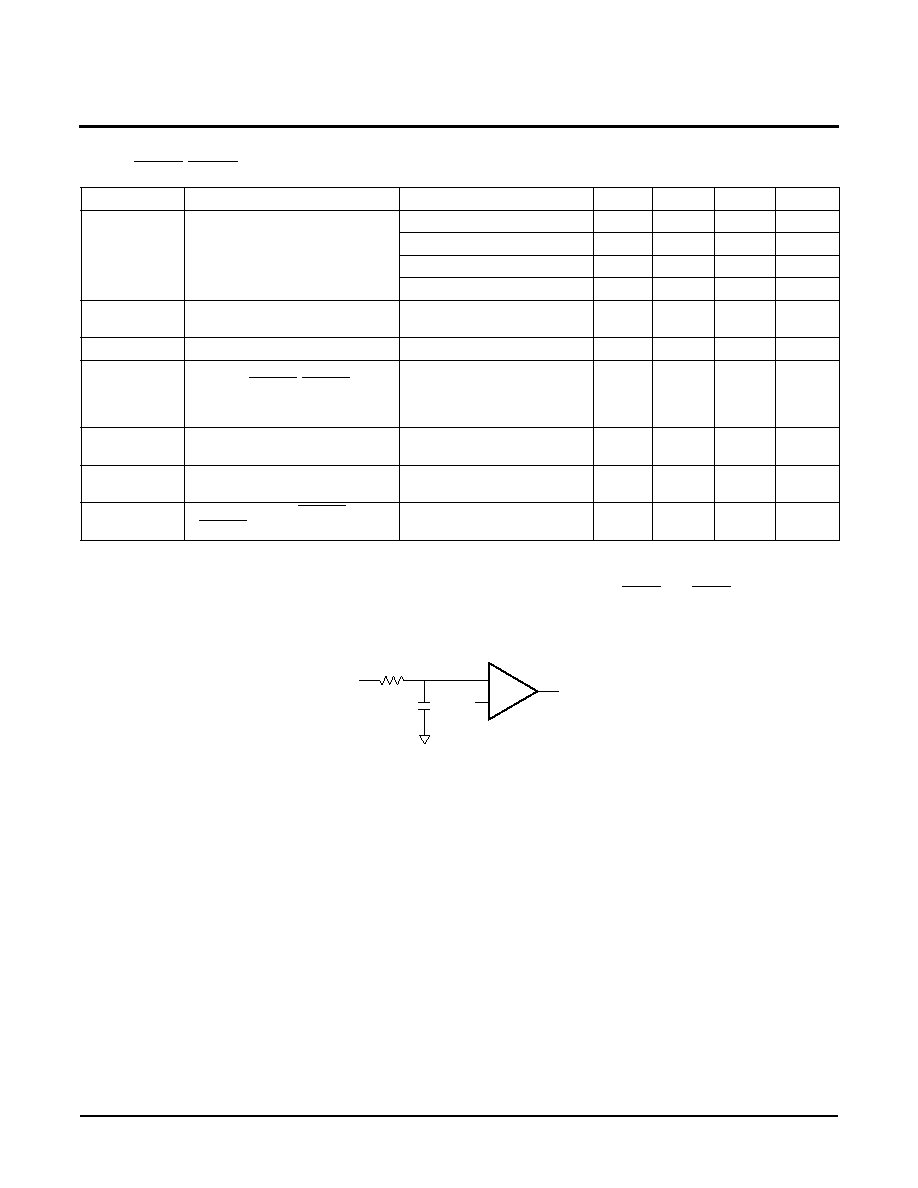
X4023x
≠ Preliminary Information
Characteristics subject to change without notice.
35 of 39
REV 1.0.4 7/12/01
www.xicor.com
RESET, V2FAIL, V3FAIL OUTPUT TIMING. (See Figure 30, Figure 31, Figure 32)
Notes: 1.
See Figure 31 for timing diagram.
Notes: 2.
See Figure 25 for equivalent load.
Notes: 3.
This parameter describes the lowest possible V
CC
level for which the outputs RESET, V2FAIL, and V3FAIL will be correct with
respect to their inputs (V
CC
, V2MON, V3MON).
Notes: 4.
From MR rising edge crossing V
IH
, to RESET rising edge crossing V
OH
.
Notes: 5.
Equivalent input circuit for V
XMON
Symbol
Description
Condition
Min.
Typ.
Max.
Units
t
PURST
Power On Reset delay time
PUP1= 0, PUP0= 0
25
50
75
ms
PUP1= 0, PUP0= 1
50
100
150
ms
PUP1= 1, PUP0= 0
100
200
300
ms
PUP1= 1, PUP0= 1
150
300
450
ms
t
MRD
(31)(2)
MR to RESET propagation
delay
See
(1)
,
(2)
,
(4)
.
5
µs
t
MRDPW
MR pulse width
500
ns
t
RPDx
V
CC
, V2MON, V3MON to
RESET,
V2FAIL
,
V3FAIL
propagation
delay (respectively)
See (5)
20
µs
t
Fx
V
CC
, V2MON, V3MON Fall
Time
20
mV/
µs
t
Rx
V
CC
, V2MON, V3MON Rise
Time
20
mV/
µs
V
RVALID
V
CC
for RESET,
V2FAIL
,
V3FAIL
Valid
(3)
.
1
V
+
≠
t
RPDX
= 20µs worst case
V
XMON
V
REF
OUTPUT

X4023x
≠ Preliminary Information
Characteristics subject to change without notice.
36 of 39
REV 1.0.4 7/12/01
www.xicor.com
APPENDIX 1
DCP1 (100 Tap) Tap position to Data Byte translation Table
Tap
Position
Data Byte
Decimal
Binary
0
0
0000 0000
1
1
0000 0001
.
.
.
.
.
.
23
23
0001 0111
24
24
0001 1000
25
56
0011 1000
26
55
0011 0111
.
.
.
.
.
.
48
33
0010 0001
49
32
0010 0000
50
64
0100 0000
51
65
0100 0001
.
.
.
.
.
.
73
87
0101 0111
74
88
0101 1000
75
120
0111 1000
76
119
0111 0111
.
.
.
.
.
.
98
97
0110 0001
99
96
0110 0000

X4023x
≠ Preliminary Information
Characteristics subject to change without notice.
37 of 39
REV 1.0.4 7/12/01
www.xicor.com
APPENDIX 2
DCP1 (100 Tap) tap position to Data Byte translation algorithm example.
unsigned DCP1_TAP_Position(int tap_pos)
{
int block;
int i;
int offset;
int wcr_val;
offset
= 0;
block
= tap_pos / 25;
if (block < 0) return ((unsigned)0);
else if (block <= 3)
{
switch(block)
{
case (0): return ((unsigned)tap_pos) ;
case (1):
{
wcr_val = 56;
offset = tap_pos - 25;
for (i=0; i<= offset; i++) wcr_val-- ;
return ((unsigned) wcr_val);
}
case (2):
{
wcr_val = 64;
offset = tap_pos - 50;
for (i=0; i<= offset; i++) wcr_val++ ;
return ((unsigned) wcr_val);
}
case (3):
{
wcr_val = 120;
offset = tap_pos - 75;
for (i=0; i<= offset; i++) wcr_val-- ;
return ((unsigned) wcr_val);
}
}
}
return((unsigned)01100000);
}

X4023x
≠ Preliminary Information
Characteristics subject to change without notice.
38 of 39
REV 1.0.4 7/12/01
www.xicor.com
16-Lead Plastic, SOIC (300-mil body), Package Code S16
NOTE: ALL DIMENSIONS IN INCHES (IN PARENTHESES IN MILLIMETERS)
0.014 (0.35)
0.020 (0.51)
PIN 1
PIN 1 INDEX
0.050 (1.27)
0.403 (10.2 )
0.413 ( 10.5)
(4X) 7∞
0.420"
0.050" Typical
0.030" Typical
16 Places
FOOTPRINT
0.010 (0.25)
0.020 (0.50)
0.0075 (0.19)
0.010 (0.25)
0
∞ ≠ 8∞
X 45
∞
0.050"
Typical
0.290 (7.37)
0.299 (7.60)
0.393 (10.00)
0.420 (10.65)
0.003 (0.10)
0.012 (0.30)
0.092 (2.35)
0.105 (2.65)
0.015 (0.40)
0.050 (1.27)

X4023x
≠ Preliminary Information
Characteristics subject to change without notice.
39 of 39
REV 1.0.4 7/12/01
www.xicor.com
Device
Preset (Factory Shipped) V
TRIPx
Threshold
Levels (x=1,2,3)
A = Optimized for 3.3 V system monitoring
3.3 ±10%, 2.5 ±10%, 1.8 V +10%/≠0%
B = Optimized for 5 V system monitoring
5.0 ±10%, 3.3 ±10%, 1.8 V +10%/≠0%
Temperature Range
I = Industrial ≠40
∞C to +85∞C
Package
S16 = 16-Lead Widebody SOIC (300 mil)
X4023x
P
T
-
y
For details of preset threshold values
,
See "D.C. OPERATING CHARACTERISTICS"
ORDERING INFORMATION
x
DEVICE
1
X40231
3
X40233
5
X40235
7
X40237
9
X40239
©Xicor, Inc. 2001 Patents Pending
LIMITED WARRANTY
Devices sold by Xicor, Inc. are covered by the warranty and patent indemnification provisions appearing in its Terms of Sale only. Xicor, Inc. makes no warranty,
express, statutory, implied, or by description regarding the information set forth herein or regarding the freedom of the described devices from patent infringement.
Xicor, Inc. makes no warranty of merchantability or fitness for any purpose. Xicor, Inc. reserves the right to discontinue production and change specifications and prices
at any time and without notice.
Xicor, Inc. assumes no responsibility for the use of any circuitry other than circuitry embodied in a Xicor, Inc. product. No other circuits, patents, or licenses are implied.
COPYRIGHTS AND TRADEMARKS
Xicor, Inc., the Xicor logo, E
2
POT, XDCP, XBGA, AUTOSTORE, Direct Write cell, Concurrent Read-Write, PASS, MPS, PushPOT, Block Lock, IdentiPROM,
E
2
KEY, X24C16, SecureFlash, and SerialFlash are all trademarks or registered trademarks of Xicor, Inc. All other brand and product names mentioned herein are
used for identification purposes only, and are trademarks or registered trademarks of their respective holders.
U.S. PATENTS
Xicor products are covered by one or more of the following U.S. Patents: 4,326,134; 4,393,481; 4,404,475; 4,450,402; 4,486,769; 4,488,060; 4,520,461; 4,533,846;
4,599,706; 4,617,652; 4,668,932; 4,752,912; 4,829,482; 4,874,967; 4,883,976; 4,980,859; 5,012,132; 5,003,197; 5,023,694; 5,084,667; 5,153,880; 5,153,691;
5,161,137; 5,219,774; 5,270,927; 5,324,676; 5,434,396; 5,544,103; 5,587,573; 5,835,409; 5,977,585. Foreign patents and additional patents pending.
LIFE RELATED POLICY
In situations where semiconductor component failure may endanger life, system designers using this product should design the system with appropriate error detection
and correction, redundancy and back-up features to prevent such an occurrence.
Xicor's products are not authorized for use in critical components in life support devices or systems.
1. Life support devices or systems are devices or systems which, (a) are intended for surgical implant into the body, or (b) support or sustain life, and whose failure to
perform, when properly used in accordance with instructions for use provided in the labeling, can be reasonably expected to result in a significant injury to the user.
2. A critical component is any component of a life support device or system whose failure to perform can be reasonably expected to cause the failure of the life
support device or system, or to affect its safety or effectiveness.