REV 1.1.15 2/11/04
Characteristics subject to change without notice.
1 of 23
www.xicor.com
64K
X40626
8K x 8 Bit
Dual Voltage CPU Supervisor with 64K Serial EEPROM
FEATURES
∑ Dual voltage monitoring
--V
2Mon
operates independent of V
CC
∑ Watchdog timer with selectable timeout intervals
∑ Low V
CC
detection and reset assertion
--Four standard reset threshold voltages
--User programmable V
TRIP
threshold
--Reset signal valid to V
CC
=1V
∑ Low power CMOS
--20µA max standby current, watchdog on
--1µA standby current, watchdog OFF
∑ 64Kbits of EEPROM
--64 byte page size
∑ Built-in inadvertent write protection
--Power-up/power-down protection circuitry
--Protect 0, 1/4, 1/2, all or 64, 128, 256 or 512
bytes of EEPROM array with programmable
Block Lock
TM
protection
∑ 400kHz 2-wire interface
--Slave addressing supports up to 4 devices on
the same bus
∑ 2.7V to 5.5V power supply operation
∑ Available Packages
--14-lead SOIC
--14-lead TSSOP
DESCRIPTION
The X40626 combines four popular functions, Power-on
Reset Control, Watchdog Timer, Dual Supply Voltage
Supervision, and Serial EEPROM Memory in one pack-
age. This combination lowers system cost, reduces
board space requirements, and increases reliability.
Applying power to the device activates the power on
reset circuit which holds RESET active for a period of
time. This allows the power supply and oscillator to stabi-
lize before the processor can execute code.
The Watchdog Timer provides an independent protection
mechanism for microcontrollers. When the microcontrol-
ler fails to restart a timer within a selectable time-out
interval, the device activates the RESET signal. The user
selects the interval from three preset values. Once
selected, the interval does not change, even after cycling
the power.
The device's low V
CC
detection circuitry protects the
user's system from low voltage conditions, resetting the
system when V
CC
falls below the set minimum V
CC
trip
point. RESET is asserted until V
CC
returns to proper
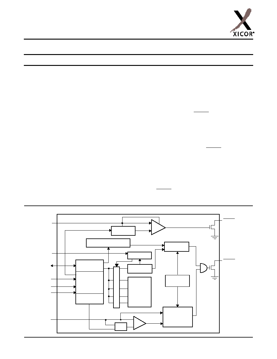
BLOCK DIAGRAM
Watchdog
Timer Reset
Data
Register
Command
Decode &
Control
Logic
SDA
SCL
V
CC
Reset &
Watchdog
Timebase
Power on and
Generation
V
TRIP
+
-
RESET
Reset
Low Voltage
Status
Register
Protect Logic
64KB
Watchdog Transition
Detector
WP
V
CC
Threshold
Reset logic
Bloc
k Loc
k Control
S0
S1
V2 Monitor
Logic
+
-
V
TRIP2
V2MON
V2FAIL
EEPROM
Array
Preliminary Information

X40626
REV 1.1.15 2/11/04
Characteristics subject to change without notice.
2 of 23
www.xicor.com
operating level and stabilizes. Four industry standard Vtrip
thresholds are available. However, Xicor's unique circuits
allow the threshold to be reprogrammed to meet custom
requirements or to fine-tune the threshold for applications
requiring higher precision.
The memory portion of the device is a CMOS Serial
EEPROM array with Xicor's Block Lock
TM
Protection. The
array is internally organized as 64 bytes per page. The
device features an 2-wire interface and software protocol
allowing operation on an I
2
C bus.
The device utilizes Xicor's proprietary Direct Write
TM
cell,
providing a minimum endurance of 100,000 page write
cycles and a minimum data retention of 100 years.
PIN CONFIGURATION
S
1
V
SS
V
CC
V2MON
WP
3
2
4
1
12
13
11
14
14 Pin SOIC/TSSOP
S
0
NC
RESET
6
5
7
9
10
8
NC
SDA
SCL
V2FAIL
NC
NC
PIN FUNCTION
Pin Name
Function
1, 4, 6, 13
NC
No Internal Connections
2
S
0
Device Select Input
3
S
1
Device Select Input
5
RESET
Reset Output
.
RESET is an active LOW, open drain output which goes active whenever V
CC
falls below the minimum V
CC
sense level. It will remain active until V
CC
rises above the min-
imum V
CC
sense level for typically 200ms. RESET goes active if the Watchdog Timer is
enabled and SDA remains either HIGH or LOW longer than the selectable Watchdog time-
out period. A falling edge on SDA, while SCL is HIGH, resets the Watchdog Timer. RESET
goes active on power up and remains active for typically 200ms after the power supply
stabilizes.
7
V
SS
Ground
8
SDA
Serial Data.
SDA is a bidirectional pin used to transfer data into and out of the device. It has
an open drain output and may be wire ORed with other open drain or open collector outputs.
This pin requires a pull up resistor and the input buffer is always active (not gated).
Watchdog Input.
A HIGH to LOW transition on the SDA (while SCL is HIGH) restarts the
Watchdog timer. The absence of a HIGH to LOW transition within the watchdog time-out
period results in RESET going active.
9
SCL
Serial Clock.
The Serial Clock controls the serial bus timing for data input and output.
10
V2FAIL
V2 Voltage Fail Output.
This open drain output goes LOW when V2MON is less than
V
TRIP2
and goes HIGH when V2MON exceeds V
TRIP2
. There is no power up reset delay
circuitry on this pin. This circuit works independently from the Low V
CC
reset and battery
switch circuits. Connect V2FAIL to VSS when not used.
11
V2MON
V2 Voltage Monitor Input.
When the V2MON input is less than the V
TRIP2
voltage, V2FAIL
goes LOW. This input can monitor an unregulated power supply with an external resistor
divider or can monitor a second power supply with no external components. Connect
V2MON to V
SS
or V
CC
when not used. There is no hysteresis in the V2MON comparator
circuits.
12
WP
Write Protect.
WP HIGH used in conjunction with WPEN bit prevents writes to the control
register.
14
V
CC
Supply Voltage

X40626
REV 1.1.15 2/11/04
Characteristics subject to change without notice.
3 of 23
www.xicor.com
PRINCIPLES OF OPERATION
Power On Reset
Application of power to the X40626 activates a Power
On Reset Circuit that pulls the RESET pin active. This
signal provides several benefits.
≠ It prevents the system microprocessor from starting
to operate with insufficient voltage.
≠ It prevents the processor from operating prior to sta-
bilization of the oscillator.
≠ It allows time for an FPGA to download its configura-
tion prior to initialization of the circuit.
≠ It prevents communication to the EEPROM, greatly
reducing the likelihood of data corruption on power up.
When V
CC
exceeds the device V
TRIP
threshold value
for t
PURST
(200ms nominal) the circuit releases
RESET allowing the system to begin operation.
LOW VOLTAGE MONITORING
During operation, the X40626 monitors the V
CC
level
and asserts RESET if supply voltage falls below a pre-
set minimum V
TRIP
. The RESET signal prevents the
microprocessor from operating in a power fail or brown-
out condition. The RESET signal remains active until
the voltage drops below 1V. It also remains active until
V
CC
returns and exceeds V
TRIP
for 200ms.
WATCHDOG TIMER
The Watchdog Timer circuit monitors the microprocessor
activity by monitoring the SDA and SCL pins. The
microprocessor must toggle the SDA pin HIGH to LOW
periodically, while SCL is HIGH (this is a start bit) prior to
the expiration of the watchdog time-out period to prevent
a RESET signal. The state of two nonvolatile control bits
in the Status Register determine the watchdog timer
period. The microprocessor can change these watchdog
bits, or they may be "locked" by tying the WP pin HIGH.
EEPROM INADVERTENT WRITE PROTECTION
When RESET goes active as a result of a low voltage
condition or Watchdog Timer Time-Out, any in-progress
communications are terminated. While RESET is
active, no new communications are allowed and no
non-volatile write operation can start. Non-volatile
writes in-progress when RESET goes active are
allowed to finish.
Additional protection mechanisms are provided with
memory Block Lock and the Write Protect (WP) pin.
These are discussed elsewhere in this document.
V
CC
/V
2MON
THRESHOLD RESET PROCEDURE
The X40626 is shipped with a standard V
CC
threshold
(V
TRIP
) voltage. This value will not change over normal
operating and storage conditions. However, in applica-
tions where the standard V
TRIP
is not exactly right, or if
higher precision is needed in the V
TRIP
value, the
X40626 threshold may be adjusted. The procedure is
described below, and uses the application of a nonvola-
tile control signal.
Setting the V
TRIP
Voltage
This procedure is used to set the V
TRIP
to a higher or
lower voltage value. It is necessary to reset the trip
point before setting the new value.
The V
CC
and V2MON must be tied together during this
sequence.
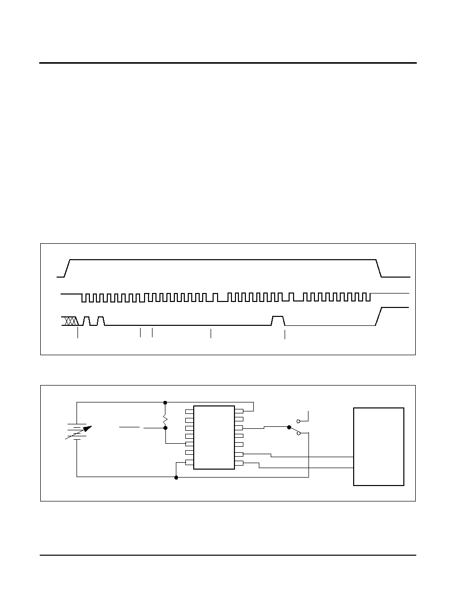
Figure 1. Set V
TRIP
Level Sequence (V
CC
/V
2MON
= desired V
TRIP
values, WP = 12-15V when WEL bit set)
0 1 2 3 4 5 6 7
SCL
SDA
A0H
0 1 2 3 4 5 6 7
00H
WP
V
P
= 12-15V
0 1 2 3 4 5 6 7
xxH*
0 1 2 3 4 5 6 7
00H
*for V
VTRIP2
address is 0DH
for V
TRIP
address is 01H
X40626
REV 1.1.15 2/11/04
Characteristics subject to change without notice.
4 of 23
www.xicor.com
To set the new V
TRIP
voltage, start by setting the WEL
bit in the control register, then apply the desired V
TRIP
threshold voltage to the V
CC
pin and the programming
voltage, V
P
,
to the WP pin and 2 byte address and 1
byte of "00" data. The stop bit following a valid write
operation initiates the V
TRIP
programming sequence.
Bring WP
LOW to complete the operation.
Resetting the V
TRIP
Voltage
This procedure is used to set the V
TRIP
to a "native"
voltage level. For example, if the current V
TRIP
is 4.4V
and the new V
TRIP
must be 4.0V, then the V
TRIP
must
be reset. When V
TRIP
is reset, the new V
TRIP
is some-
thing less than 1.7V. This procedure must be used to
set the voltage to a lower value.
To reset the new V
TRIP
voltage start by setting the WEL
bit in the control register, apply the desired V
TRIP
threshold voltage to the V
CC
pin and the programming
voltage, V
P
, to the WP pin and 2 byte address and 1
byte of "00" data. The stop bit of a valid write operation
initiates the V
TRIP
programming sequence. Bring WP
LOW to complete the operation.
Figure 2. Reset V
TRIP
Level Sequence (V
CC
/V
2MON
> 3V, WP = 12-15V, WEL bit set)
Figure 3. Sample V
TRIP
Reset Circuit
0 1 2 3 4 5 6 7
SCL
SDA
A0H
0 1 2 3 4 5 6 7
00H
WP
V
P
= 12-15V
0 1 2 3 4 5 6 7
xxH*
0 1 2 3 4 5 6 7
00H
*for V
TRIP2
address is 0FH
for V
TRIP
address is 03H
1
2
5
7
14
12
9
8
X40626
V
TRIP
Adj.
V
P
RESET
4.7K
SDA
SCL
µC
Adjust
Run
6
3
13
4
X40626
REV 1.1.15 2/11/04
Characteristics subject to change without notice.
5 of 23
www.xicor.com
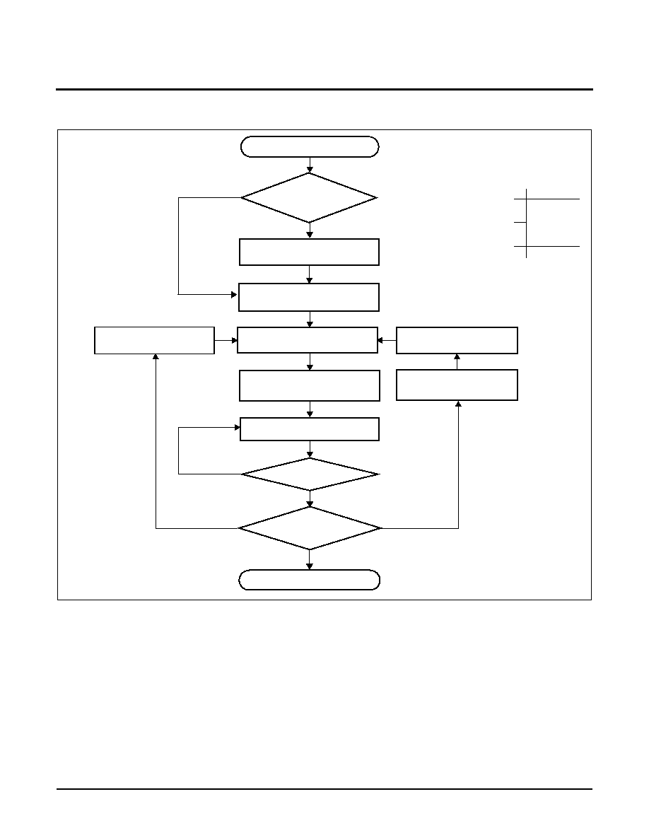
Figure 4. V
TRIP
Programming Sequence
V
TRIPX
Programming
Apply V
CC
and Voltage
Decrease V
X
Actual V
TRIPX -
Desired V
TRIPX
DONE
Set Higher V
X
Sequence
Error < MDE
≠
| Error | < | MDE |
YES
NO
Error > MDE
+
> Desired V
TRIPX
to V
X
Desired
Present Value
V
TRIPX
Execute
No
YES
Set V
X
= Desired V
TRIPX
Execute
Set Higher V
TRIPX
Sequence
New V
X
applied =
Old V
X
applied + | Error |
New V
X
applied =
Old V
X
applied - | Error |
Execute Reset V
TRIPX
Sequence
Output Switches?
Let: MDE = Maximum Desired Error
Vx = V
CC
, V2MON
MDE
+
Desired Value
MDE
≠
Acceptable
Error Range
Error = Actual - Desired
X40626
REV 1.1.15 2/11/04
Characteristics subject to change without notice.
6 of 23
www.xicor.com
Control Register
The Control Register provides the user a mechanism
for changing the Block Lock and Watchdog Timer set-
tings. The Block Lock and Watchdog Timer bits are
nonvolatile and do not change when power is removed.
The Control Register is accessed at address FFFFh. It
can only be modified by performing a byte write opera-
tion directly to the address of the register and only one
data byte is allowed for each register write operation.
Prior to writing to the Control Register, the WEL and
RWEL bits must be set using a two step process, with
the whole sequence requiring 3 steps. See "Writing to
the Control Register" below.
The user must issue a stop after sending this byte to
the register to initiate the nonvolatile cycle that stores
WD1, WD0, BP2, BP1, and BP0. The X40626 will not
acknowledge any data bytes written after the first byte
is entered.
The state of the Control Register can be read at any
time by performing a random read at address FFFFh.
Only one byte is read by each register read operation.
The X40626 resets itself after the first byte is read. The
master should supply a stop condition to be consistent
with the bus protocol, but a stop is not required to end
this operation.
RWEL: Register Write Enable Latch (Volatile)
The RWEL bit must be set to "1" prior to a write to the
Control Register.
WEL: Write Enable Latch (Volatile)
The WEL bit controls the access to the memory and to
the Register during a write operation. This bit is a vola-
tile latch that powers up in the LOW (disabled) state.
While the WEL bit is LOW, writes to any address,
including any control registers will be ignored (no
acknowledge will be issued after the Data Byte). The
WEL bit is set by writing a "1" to the WEL bit and zeroes
to the other bits of the control register. Once set, WEL
remains set until either it is reset to 0 (by writing a "0" to
the WEL bit and zeroes to the other bits of the control
register) or until the part powers up again. Writes to the
WEL bit do not cause a nonvolatile write cycle, so the
device is ready for the next operation immediately after
the stop condition.
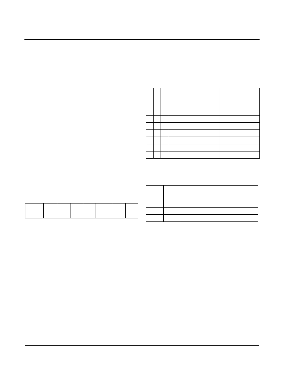
BP2, BP1, BP0: Block Protect Bits - (Nonvolatile)
The Block Protect Bits, BP2, BP1 and BP0, determine
which blocks of the array are write protected. A write to
a protected block of memory is ignored. The block pro-
tect bits will prevent write operations to one of eight
segments of the array.
WD1, WD0: Watchdog Timer Bits
The bits WD1 and WD0 control the period of the
Watchdog Timer. The options are shown below.
Write Protect Enable
These devices have an advanced Block Lock scheme
that protects one of eight blocks of the array when
enabled. It provides hardware write protection through
the use of a WP pin and a nonvolatile Write Protect
Enable (WPEN) bit. Four of the 8 protected blocks
match the original Block Lock segments and this pro-
tection scheme is fully compatible with the current
devices using 2 bits of block lock control (assuming the
BP2 bit is set to 0).
The Write Protect (WP) pin and the Write Protect
Enable (WPEN) bit in the Control Register control the
programmable Hardware Write Protect feature. Hard-
ware Write Protection is enabled when the WP pin and
the WPEN bit are HIGH and disabled when either the
WP pin or the WPEN bit is LOW. When the chip is Hard-
ware Write Protected, nonvolatile writes as well as to the
block protected sections in the memory array cannot be
written. Only the sections of the memory array that are
7
6
5
4
3
2
1
0
WPEN
WD1 WD0 BP1
BP0 RWEL WEL BP2
BP2
BP1
BP0
Protected Addresses
(Size)
Array Lock
0
0
0
None (factory setting)
None
0
0
1
1800h - 1FFFH
(2K bytes
)
Upper 1/4 (Q4)
0
1
0
1000h - 1FFFH
(4K bytes
)
Upper 1/2 (Q3,Q4)
0
1
1
0000h - 1FFFH
(8K bytes)
Full Array (All)
1
0
0
000h - 03FH
(64 bytes)
First Page (P1)
1
0
1
000h - 07FH
(128 bytes)
First 2 pgs (P2)
1
1
0
000h - 0FFH
(256 bytes)
First 4 pgs (P4)
1
1
1
000h - 1FFH
(512 bytes)
First 8 Pgs (P8)
WD1
WD0
Typ. Watchdog Time-out Period
0
0
1.4 Seconds
0
1
600 milliseconds
1
0
200 milliseconds
1
1
Disabled (factory setting)
X40626
REV 1.1.15 2/11/04
Characteristics subject to change without notice.
7 of 23
www.xicor.com
not block protected can be written. Note that since the
WPEN bit is write protected, it cannot be changed back
to a LOW state; so write protection is enabled as long
as the WP pin is held HIGH.
Table 1. Write Protect Enable Bit and WP Pin Function
WP
WPEN
Memory Array not
Block Protected
Memory Array
Block Protected
Block Protect
Bits
WPEN Bit
Protection
LOW
X
Writes OK
Writes Blocked
Writes OK
Writes OK
Software
HIGH
0
Writes OK
Writes Blocked
Writes OK
Writes OK
Software
HIGH
1
Writes OK
Writes Blocked
Writes Blocked
Writes Blocked
Hardware
Writing to the Control Register
Changing any of the nonvolatile bits of the control reg-
ister requires the following steps:
≠ Write a 02H to the Control Register to set the Write
Enable Latch (WEL). This is a volatile operation, so
there is no delay after the write. (Operation pro-
ceeded by a start and ended with a stop).
≠ Write a 06H to the Control Register to set both the
Register Write Enable Latch (RWEL) and the WEL
bit. This is also a volatile cycle. The zeros in the data
byte are required. (Operation proceeded by a start
and ended with a stop).
≠ Write a value to the Control Register that has all the
control bits set to the desired state. This can be rep-
resented as 0xys t01r in binary, where xy are the WD
bits, and rst are the BP bits. (Operation preceeded by
a start and ended with a stop). Since this is a nonvol-
atile write cycle it will take up to 10ms to complete.
The RWEL bit is reset by this cycle and the sequence
must be repeated to change the nonvolatile bits
again. If bit 2 is set to `1' in this third step (0xys t11r)
then the RWEL bit is set, but the WD1, WD0, BP2,
BP1 and BP0 bits remain unchanged. Writing a sec-
ond byte to the control register is not allowed. Doing
so aborts the write operation and returns a NACK.
≠ A read operation occurring between any of the previ-
ous operations will not interrupt the register write
operation.
≠ The RWEL bit cannot be reset without writing to the
nonvolatile control bits in the control register, power
cycling the device or attempting a write to a write pro-
tected block.
To illustrate, a sequence of writes to the device consist-
ing of [02H, 06H, 02H] will reset all of the nonvolatile
bits in the Control Register to 0. A sequence of [02H,
06H, 06H] will leave the nonvolatile bits unchanged and
the RWEL bit remains set.
SERIAL INTERFACE
Serial Interface Conventions
The device supports a bidirectional bus oriented proto-
col. The protocol defines any device that sends data
onto the bus as a transmitter, and the receiving device
as the receiver. The device controlling the transfer is
called the master and the device being controlled is
called the slave. The master always initiates data trans-
fers, and provides the clock for both transmit and
receive operations. Therefore, the devices in this family
operate as slaves in all applications.
Serial Clock and Data
Data states on the SDA line can change only during
SCL LOW. SDA state changes during SCL HIGH are
reserved for indicating start and stop conditions. See
Figure 5.
X40626
REV 1.1.15 2/11/04
Characteristics subject to change without notice.
8 of 23
www.xicor.com
Figure 5. Valid Data Changes on the SDA Bus
SCL
SDA
Data Stable
Data Change
Data Stable
Serial Start Condition
All commands are preceded by the start condition,
which is a HIGH to LOW transition of SDA when SCL is
HIGH. The device continuously monitors the SDA and
SCL lines for the start condition and will not respond to
any command until this condition has been met. See
Figure 6.
Serial Stop Condition
All communications must be terminated by a stop con-
dition, which is a LOW to HIGH transition of SDA when
SCL is HIGH. The stop condition is also used to place
the device into the Standby power mode after a read
sequence. A stop condition can only be issued after the
transmitting device has released the bus. See Figure 6.
Figure 6. Valid Start and Stop Conditions
SCL
SDA
Start
Stop
Serial Acknowledge
Acknowledge is a software convention used to indicate
successful data transfer. The transmitting device, either
master or slave, will release the bus after transmitting
eight bits. During the ninth clock cycle, the receiver will
pull the SDA line LOW to acknowledge that it received
the eight bits of data. Refer to Figure 7.
The device will respond with an acknowledge after rec-
ognition of a start condition and if the correct Device
Identifier and Select bits are contained in the Slave
Address Byte. If a write operation is selected, the
device will respond with an acknowledge after the
receipt of each subsequent eight bit word. The device
will acknowledge all incoming data and address bytes,
except for the Slave Address Byte when the Device
Identifier and/or Select bits are incorrect.
In the read mode, the device will transmit eight bits of
data, release the SDA line, then monitor the line for an
acknowledge. If an acknowledge is detected and no
stop condition is generated by the master, the device
will continue to transmit data. The device will terminate
further data transmissions if an acknowledge is not
detected. The master must then issue a stop condition
to return the device to Standby mode and place the
device into a known state.
X40626
REV 1.1.15 2/11/04
Characteristics subject to change without notice.
9 of 23
www.xicor.com
Figure 7. Acknowledge Response From Receiver
Data Output
from Transmitter
Data Output
from Receiver
8
1
9
Start
Acknowledge
SCL from
Master
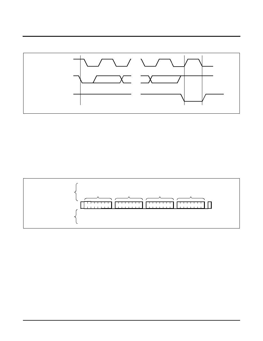
Serial Write Operations
Byte Write
For a write operation, the device requires the Slave
Address Byte and a Word Address Byte. This gives the
master access to any one of the words in the array. After
receipt of the Word Address Byte, the device responds
with an acknowledge, and awaits the next eight bits of
data. After receiving the 8 bits of the Data Byte, the
device again responds with an acknowledge. The mas-
ter then terminates the transfer by generating a stop
condition, at which time the device begins the internal
write cycle to the nonvolatile memory. During this inter-
nal write cycle, the device inputs are disabled, so the
device will not respond to any requests from the master.
The SDA output is at high impedance. See Figure 8.
Figure 8. Byte Write Sequence
Signals from
the Master
SDA Bus
Signals from
the Slave
S
T
A
R
T
Slave
Address
S
T
O
P
A
C
K
A
C
K
A
C
K
A
C
K
Byte 1
Data
1 0 1 0 0
Word Address
Byte 0
S
P
0
Word Address
S
1
S
0
A write to a protected block of memory will suppress
the acknowledge bit.
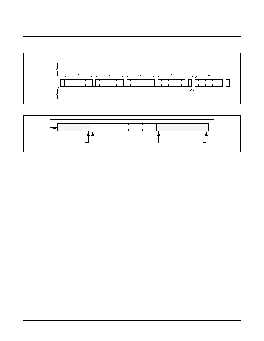
Page Write
The device is capable of a page write operation. It is
initiated in the same manner as the byte write opera-
tion; but instead of terminating the write cycle after the
first data byte is transferred, the master can transmit an
unlimited number of 8-bit bytes. After the receipt of
each byte, the device will respond with an acknowl-
edge, and the address is internally incremented by
one. The page address remains constant. When the
counter reaches the end of the page, it "rolls over" and
goes back to `0' on the same page. This means that the
master can write 64 bytes to the page starting at any
location on that page. If the master begins writing at
location 60, and loads 12 bytes, then the first 4 bytes
are written to locations 60 through 63, and the last 8
bytes are written to locations 0 through 7. Afterwards,
the address counter would point to location 8 of the
page that was just written. If the master supplies more
than 64 bytes of data, then new data over-writes the
previous data, one byte at a time.
X40626
REV 1.1.15 2/11/04
Characteristics subject to change without notice.
10 of 23
www.xicor.com
Figure 9. Page Write Operation
Figure 10. Writing 12 bytes to a 64-byte page starting at location 60 (Wrap around).
S
T
A
R
T
S
T
O
P
A
C
K
A
C
K
A
C
K
A
C
K
A
C
K
Data
(0)
(n)
0
S
P
Data
1 0 1 0
(I
n 63)
Signals from
the Master
SDA Bus
Signals from
the Slave
Slave
Address
Byte 1
Word Address
Byte 0
Word Address
0
S
1
S
0
address
address
60
4 Bytes
63
8 Bytes
address
= 7
address pointer
ends here
Addr = 8
The master terminates the Data Byte loading by issuing
a stop condition, which causes the device to begin the
nonvolatile write cycle. As with the byte write operation,
all inputs are disabled until completion of the internal
write cycle. See Figure 9 for the address, acknowledge,
and data transfer sequence.
Stops and Write Modes
Stop conditions that terminate write operations must be
sent by the master after sending at least 1 full data byte
plus the subsequent ACK signal. If a stop is issued in
the middle of a data byte, or before 1 full data byte plus
its associated ACK is sent, then the device will reset
itself without performing the write. The contents of the
array will not be effected.
Acknowledge Polling
The disabling of the inputs during nonvolatile cycles
can be used to take advantage of the typical 5mS write
cycle time. Once the stop condition is issued to indicate
the end of the master's byte load operation, the device
initiates the internal nonvolatile cycle. Acknowledge
polling can be initiated immediately. To do this, the
master issues a start condition followed by the Slave
Address Byte for a write or read operation. If the device
is still busy with the nonvolatile cycle then no ACK will
be returned. If the device has completed the write oper-
ation, an ACK will be returned and the host can then
proceed with the read or write operation. Refer to the
flow chart in Figure 11.
X40626
REV 1.1.15 2/11/04
Characteristics subject to change without notice.
11 of 23
www.xicor.com
Figure 11. Acknowledge Polling Sequence
Serial Read Operations
Read operations are initiated in the same manner as
write operations with the exception that the R/W bit of
the Slave Address Byte is set to one. There are three
basic read operations: Current Address Reads, Ran-
dom Reads, and Sequential Reads.
Current Address Read
Internally the device contains an address counter that
maintains the address of the last word read incre-
mented by one. Therefore, if the last read was to
address n, the next read operation would access data
from address n+1. On power up, the address in the
address counter is 00H.
Upon receipt of the Slave Address Byte with the R/W
bit set to one, the device issues an acknowledge and
then transmits the eight bits of the Data Byte. The mas-
ter terminates the read operation when it does not
respond with an acknowledge during the ninth clock
and then issues a stop condition. Refer to Figure 12 for
the address, acknowledge, and data transfer
sequence.
It should be noted that the ninth clock cycle of the read
operation is not a "don't care." To terminate a read
operation, the master must either issue a stop condi-
tion during the ninth cycle or hold SDA HIGH during the
ninth clock cycle and then issue a stop condition.
ACK
returned?
Issue Slave Address
Byte (Read or Write)
Byte load completed
by issuing STOP.
Enter ACK Polling
Issue STOP
Issue START
NO
YES
Nonvolatile Cycle
complete. Continue
command sequence?
Issue STOP
NO
Continue Normal
Read or Write
Command Sequence
PROCEED
YES
Figure 12. Current Address Read Sequence
S
t
a
r
t
S
t
o
p
Slave
Address
Data
SDA Bus
Signals from
the Slave
Signals from
the Master
A
C
K
S
0
S
1
1
1 0 1 0 0

X40626
REV 1.1.15 2/11/04
Characteristics subject to change without notice.
12 of 23
www.xicor.com
Random Read
Random read operation allows the master to access
any memory location in the array. Prior to issuing the
Slave Address Byte with the R/W bit set to one, the
master must first perform a "dummy" write operation.
The master issues the start condition and the Slave
Address Byte, receives an acknowledge, then issues
the Word Address Bytes. After acknowledging receipts
of the Word Address Bytes, the master immediately
issues another start condition and the Slave Address
Byte with the R/W bit set to one. This is followed by an
acknowledge from the device and then by the eight bit
word. The master terminates the read operation by not
responding with an acknowledge and then issuing a
stop condition. Refer to Figure 13 for the address,
acknowledge, and data transfer sequence.
Figure 13. Random Address Read Sequence
Signals from
the Master
SDA Bus
Signals from
the Slave
S
T
A
R
T
S
T
O
P
A
C
K
A
C
K
A
C
K
0
S
T
A
R
T
1
Data
A
C
K
S
P
S
1 0 1 0
Slave
Address
Byte 1
Word Address
Byte 0
Word Address
Slave
Address
S
1
S
0
1 0 1 0
S
1
S
0
0
0
There is a similar operation, called "Set Current
Address" where the device does no operation, but
enters a new address into the address counter if a stop
is issued instead of the second start shown in Figure
13. The device goes into standby mode after the stop
and all bus activity will be ignored until a start is
detected. The next Current Address Read operation
reads from the newly loaded address. This operation
could be useful if the master knows the next address it
needs to read, but is not ready for the data.
Sequential Read
Sequential reads can be initiated as either a current
address read or random address read. The first Data
Byte is transmitted as with the other modes; however,
the master now responds with an acknowledge, indi-
cating it requires additional data. The device continues
to output data for each acknowledge received. The
master terminates the read operation by not respond-
ing with an acknowledge and then issuing a stop condi-
tion.
The data output is sequential, with the data from
address n followed by the data from address n + 1. The
address counter for read operations increments
through all page and column addresses, allowing the
entire memory contents to be serially read during one
operation. At the end of the address space the counter
"rolls over" to address 0000H and the device continues
to output data for each acknowledge received. Refer to
Figure 14 for the acknowledge and data transfer
sequence.
X40626
REV 1.1.15 2/11/04
Characteristics subject to change without notice.
13 of 23
www.xicor.com
Figure 14. Sequential Read Sequence
Data
(2)
S
t
o
p
Slave
Address
Data
(n)
A
C
K
A
C
K
SDA Bus
Signals from
the Slave
Signals from
the Master
1
Data
(n-1)
A
C
K
A
C
K
(n is any integer greater than 1)
Data
(1)
S
1
S
0
X40626 Addressing
Slave Address Byte
Following a start condition, the master must output a
Slave Address Byte. This byte consists of several parts:
≠ a device type identifier that is `1010' to access the
array
≠ one bit of `0'.
≠ next two bits are the device address. (S1 and S0)
≠ one bit of the slave command byte is a R/W bit. The
R/W bit of the Slave Address Byte defines the opera-
tion to be performed. When the R/W bit is a one, then
a read operation is selected. A zero selects a write
operation. Refer to Figure 15.
≠ After loading the entire Slave Address Byte from the
SDA bus, the device compares the input slave byte
data to the proper slave byte. Upon a correct compare,
the device outputs an acknowledge on the SDA line.
Word Address
The word address is either supplied by the master or
obtained from an internal counter. The internal counter
is 00H on a power up condition.
The master must supply the two word address byte as
shown in Figure 15.

X40626
REV 1.1.15 2/11/04
Characteristics subject to change without notice.
14 of 23
www.xicor.com
Figure 15. X40626 Addressing
R/W
S0
S1
0
1
0
1
Slave Address Byte
Device Identifier
Device Select
A8
A9
A10
A11
A12
A13
A14
A15
Word Address Byte 1
High Order Word Address
A0
A1
A2
Word Address Byte 0
Low Order Word Address
A3
A4
A5
A6
A7
D0
D1
D2
D3
D4
D5
D6
D7
Data Byte
0
Operational Notes
The device powers-up in the following state:
≠ The device is in the low power standby state.
≠ The WEL bit is set to `0'. In this state it is not possible
to write to the device.
≠ SDA pin is in the input mode.
≠ RESET Signal is active for t
PURST
.
Data Protection
The following circuitry has been included to prevent
inadvertent writes:
≠ The WEL bit must be set to allow write operations.
≠ The proper clock count and bit sequence is required
prior to the stop bit in order to start a nonvolatile write
cycle.
≠ A three step sequence is required before writing into
the Control Register to change Watchdog Timer or
Block Lock settings.
≠ The WP pin, when held HIGH, and WPEN bit at logic
HIGH will prevent all writes to the Control Register.
≠ Communication to the device is inhibited while
RESET is active and any in-progress communication
is terminated.
≠ Block Lock bits can protect sections of the memory
array from write operations.
Symbol Table
WAVEFORM
INPUTS
OUTPUTS
Must be
steady
Will be
steady
May change
from LOW
to HIGH
Will change
from LOW
to HIGH
May change
from HIGH
to LOW
Will change
from HIGH
to LOW
Don't Care:
Changes
Allowed
Changing:
State Not
Known
N/A
Center Line
is High
Impedance
X40626
REV 1.1.15 2/11/04
Characteristics subject to change without notice.
15 of 23
www.xicor.com
ABSOLUTE MAXIMUM RATINGS
Temperature under bias ................... -65∞C to +135∞C
Storage temperature ........................ -65∞C to +150∞C
Voltage on any pin with respect to VSS ....-1.0V to +7V
D.C. output current (sink).................................... 10mA
Lead temperature (soldering, 10 seconds).........300∞C
Table 2. Recommended Operating Conditions
COMMENT
Stresses above those listed under "Absolute Maximum
Ratings" may cause permanent damage to the device.
This is a stress rating only; functional operation of the
device (at these or any other conditions above those
listed in the operational sections of this specification) is
not implied. Exposure to absolute maximum rating con-
ditions for extended periods may affect device reliability.
Temp
Min.
Max.
Commercial
0∞C
70∞C
Industrial
-40∞C
+85∞C
D.C. OPERATING CHARACTERISTICS (Over the recommended operating conditions unless otherwise specified.)
Notes: (1) The device enters the Active state after any start, and remains active until: (a) 9 clock cycles later if the Device Select Bits in the
Slave Address Byte are incorrect; or (b) 200nS after a stop ending a read operation.
(2) The device enters the Active state after any start, and remains active until t
WC
after a stop ending a write operation.
(3) The device goes into Standby: (a) 200nS after any stop, except those that initiate a nonvolatile write cycle; or (b) t
WC
after a stop
that initiates a nonvolatile cycle; or 9 clock cycles after any start that is not followed by the correct Device Select Bits in the Slave
Address Byte.
Symbol
Parameter
V
CC
= 2.7 to 5.5V
Unit
Test Conditions
Min
Max
I
CC1
(1)
Active Supply Current Read
1.0
mA
V
IL
= V
CC
x 0.1, V
IH
= V
CC
x 0.9
f
SCL
= 400KHz, SDA = Open
I
CC2
(2)
Active Supply Current Write
3.0
mA
I
SB1
(2)
Standby Current DC (WDT off)
1
µA
V
SDA
=V
SCL
=V
CC
Others=GND or V
CC
I
SB2
(3)
Standby Current DC (WDT on)
30
µA
V
SDA
=V
SCL
=V
CC
Others=GND or V
CC
I
LI
Input Leakage Current
10
µA
V
IN
= GND to V
CC
I
LO
Output Leakage Current
10
µA
V
SDA
= GND to V
CC
Device is in Standby
V
IL
Input LOW Voltage
-1
V
CC
x 0.3
V
V
IH
Input HIGH Voltage
V
CC
x 0.7
V
CC
+0.5
V
V
HYS
Schmitt Trigger Input Hysteresis
Fixed input level
V
CC
related level
0.2
.05 x V
CC
V
V
V
OL
Output LOW Voltage
0.4
V
I
OL
= 1.0mA (V
CC
=3V)
I
OL
= 3.0mA (V
CC
=5V)
X40626
REV 1.1.15 2/11/04
Characteristics subject to change without notice.
16 of 23
www.xicor.com
CAPACITANCE (T
A
= 25∞C, f = 1.0 MHz, V
CC
= 5V)
Notes: (4) This parameter is periodically sampled and not 100% tested.
Symbol
Parameter
Max.
Units
Test Conditions
C
OUT
(4)
Output Capacitance (SDA, RESET, V2FAIL)
8
pF
V
OUT
= 0V
C
IN
(4)
Input Capacitance (SCL, WP, S0, S1)
6
pF
V
IN
= 0V
EQUIVALENT A.C. LOAD CIRCUIT
A.C. TEST CONDITIONS
V2MON
1.53K
V2FAIL
30pF
SDA
RESET
1533
30pF
5V
Input pulse levels
0.1V
CC
to 0.9V
CC
Input rise and fall times
10ns
Input and output timing levels
0.5V
CC
Output load
Standard Output Load
A.C. CHARACTERISTICS (Over recommended operating conditions, unless otherwise specified)
Notes: (1) Typical values are for T
A
= 25∞C and V
CC
= 5.0V
(2) Cb = total capacitance of one bus line in pF.
Symbol Parameter
Min.
Max.
Units
f
SCL
SCL Clock Frequency
0
400
KHz
t
IN
Pulse width Suppression Time at inputs
50
ns
t
AA
SCL LOW to SDA Data Out Valid
0.1
0.9
µs
t
BUF
Time the bus free before start of new transmission
1.3
µs
t
LOW
Clock LOW Time
1.3
µs
t
HIGH
Clock HIGH Time
0.6
µs
t
SU:STA
Start Condition Setup Time
0.6
µs
t
HD:STA
Start Condition Hold Time
0.6
µs
t
SU:DAT
Data In Setup Time
100
ns
t
HD:DAT
Data In Hold Time
0
µs
t
SU:STO
Stop Condition Setup Time
0.6
µs
t
DH
Data Output Hold Time
50
ns
t
R
SDA and SCL Rise Time
20 + 0.1Cb
(2)
300
ns
t
F
SDA and SCL Fall Time
20 + 0.1Cb
(2)
300
ns
t
SU:WP
WP Setup Time
0.6
µs
t
HD:WP
WP Hold Time
0
µs
Cb
Capacitive load for each bus line
400
pF
X40626
REV 1.1.15 2/11/04
Characteristics subject to change without notice.
17 of 23
www.xicor.com
TIMING DIAGRAMS
Bus Timing
WP Pin Timing
Write Cycle Timing
Nonvolatile Write Cycle Timing
Notes: (1) t
WC
is the time from a valid stop condition at the end of a write sequence to the end of the self-timed internal nonvolatile write cycle.
It is the minimum cycle time to be allowed for any nonvolatile write by the user, unless Acknowledge Polling is used.
Symbol Parameter
Min.
Typ.
(1)
Max.
Units
t
WC
(1)
Write Cycle Time
5
10
mS
t
SU:STO
t
DH
t
HIGH
t
SU:STA
t
HD:STA
t
HD:DAT
t
SU:DAT
SCL
SDA IN
SDA OUT
t
F
t
LOW
t
BUF
t
AA
t
R
t
HD:WP
SCL
SDA IN
WP
t
SU:WP
Clk 1
Clk 9
Slave Address Byte
START
SCL
SDA
t
WC
8th bit of Last Byte
ACK
Stop
Condition
Start
Condition
X40626
REV 1.1.15 2/11/04
Characteristics subject to change without notice.
18 of 23
www.xicor.com
Power-Up and Power-Down Timing
RESET Output Timing
Notes: (8) This parameter is periodically sampled and not 100% tested.
SDA vs. RESET Timing
Symbol
Parameter
Min.
Typ.
Max.
Units
t
PURST
Power-up Reset Timeout
100
200
400
ms
t
RPD
(8)
V
CC
Detect to Reset/Output (Falling Edge)
500
ns
t
F
(8)
V
CC
/V2MON Fall Time
100
µs
t
R
(8)
V
CC
/V2MON Rise Time
100
µs
V
RVALID
(8)
Reset Valid V
CC
or V2FAIL Valid V2MON
1.0
V
V
TRIP
Range
Voltage Range over which V
TRIP
/V
TRIP2
can be set
2.0
V
CC
V
V
CC
/V2MON
t
PURST
t
R
t
F
t
RPD
0 Volts
V
TRIP
/V
TRIP2
RESET/V2FAIL
V
RVALID
t
PURST
< t
WDO
t
RST
RESET
SDA
Start
t
WDO
t
RST
SCL
Timer Start
t
RSP
Timer
Restart
Timer Start
Start
X40626
REV 1.1.15 2/11/04
Characteristics subject to change without notice.
19 of 23
www.xicor.com
RESET Output Timing
V
TRIP
Programming Timing Diagram (WEL = 1)
Symbol
Parameter
Min.
Typ.
Max.
Units
t
WDO
Watchdog Timeout Period,
WD1 = 1, WD0 = 1 (factory setting)
WD1 = 1, WD0 = 0
WD1 = 0, WD0 = 1
WD1 = 0, WD0 = 0
Disabled
100
450
1.0
Disabled
200
600
1.4
Disabled
400
850
2.0
Factory Setting
ms
ms
sec
t
RST
Reset Timeout
100
250
400
ms
SCL
SDA
0001H*: set V
TRIP
00h
V
CC
/V2MON
(V
TRIP
/V
TRIP2
)
WP
t
TSU
t
THD
t
VPS
V
P
t
VPO
AS
1
S
0
00h
0 1 2
7
0
7
0
7
0
7
t
WC
Start
000DH: set V
TRIP2
0003H: Resets V
TRIP
000FH: Resets V
TRIP2
data
V
CC
/V2MON
X40626
REV 1.1.15 2/11/04
Characteristics subject to change without notice.
20 of 23
www.xicor.com
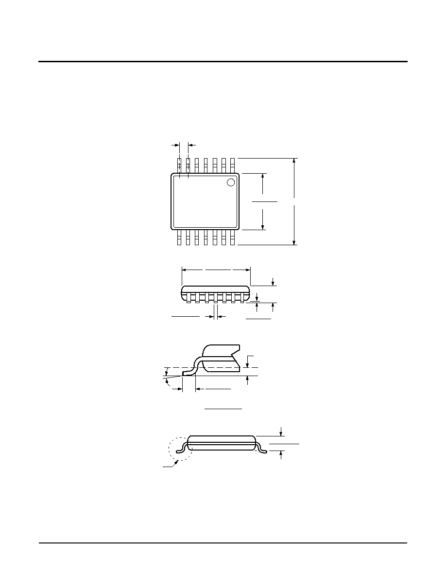
Packaging Information
0.150 (3.80)
0.158 (4.00)
0.228 (5.80)
0.244 (6.20)
0.014 (0.35)
0.020 (0.51)
Pin 1
Pin 1 Index
0.050 (1.27)
0.336 (8.55)
0.345 (8.75)
0.004 (0.10)
0.010 (0.25)
0.053 (1.35)
0.069 (1.75)
(4X) 7∞
14-Lead Plastic Small Outline Gullwing Package Type S
NOTE: ALL DIMENSIONS IN INCHES (IN PARENTHESES IN MILLIMETERS)
0.010 (0.25)
0.020 (0.50)
0.016 (0.410)
0.037 (0.937)
0.0075 (0.19)
0.010 (0.25)
0∞ ≠ 8∞
X 45∞
0.250"
0.050" Typical
0.030" Typical
14 Places
FOOTPRINT
0.050" Typical
X40626
REV 1.1.15 2/11/04
Characteristics subject to change without notice.
21 of 23
www.xicor.com
PACKAGING INFORMATION
NOTE: ALL DIMENSIONS IN INCHES (IN PARENTHESES IN MILLIMETERS)
14-Lead Plastic, TSSOP, Package Code V14
See Detail "A"
.031 (.80)
.041 (1.05)
.169 (4.3)
.177 (4.5)
.252 (6.4) BSC
.025 (.65) BSC
.193 (4.9)
.200 (5.1)
.002 (.05)
.006 (.15)
.041 (1.05)
.0075 (.19)
.0118 (.30)
0∞ - 8∞
.010 (.25)
.019 (.50)
.029 (.75)
Gage Plane
Seating Plane
Detail A (20X)
X40626
REV 1.1.15 2/11/04
Characteristics subject to change without notice.
22 of 23
www.xicor.com
Ordering Information
PART MARK INFORMATION
V
CC
Range
V
TRIP
Range
V
TRIP2
Range
Package
Operating
Temperature
Range
Part Number RESET
(Active LOW)
Park
Mark
4.5-5.5V
4.5-4.75
2.85-3.0
14L SOIC
0∞C≠70∞C
X40626S14≠4.5A
AL
-40∞C≠85∞C
X40626S14I≠4.5A
AM
14L TSSOP
0∞C≠70∞C
X40626V14≠4.5A
AL
-40∞C≠85∞C
X40626V14I≠4.5A
AM
4.5-5.5V
4.25-4.5
2.85-3.0
14L SOIC
0∞C≠70∞C
X40626S14
blank
-40∞C≠85∞C
X40626S14I
I
14L TSSOP
0∞C≠70∞C
X40626V14
blank
-40∞C≠85∞C
X40626V14I
I
2.7-5.5V
2.85-3.0
2.15-2.30
14L SOIC
0∞C≠70∞C
X40626S14≠2.7A
AN
-40∞C≠85∞C
X40626S14I≠2.7A
AP
14LTSSOP
0∞C≠70∞C
X40626V14≠2.7A
BN
-40∞C≠85∞C
X40626V14I≠2.7A
AP
2.7-5.5V
2.55-2.7
2.55-2.7
14L SOIC
0∞C≠70∞C
X40626S14≠2.7
F
-40∞C≠85∞C
X40626S14I≠2.7
G
14L TSSOP
0∞C≠70∞C
X40626V14≠2.7
F
-40∞C≠85∞C
X40626V14I≠2.7
G
14-Lead SOIC/TSSOP
X40626 X
YYWWXX
S = SOIC
WW ≠ Workweek
YY ≠ Year
V = TSSOP
XX ≠ Part Mark

X40626
LIMITED WARRANTY
Devices sold by Xicor, Inc. are covered by the warranty and patent indemnification provisions appearing in its Terms of Sale only. Xicor, Inc. makes no warranty, express,
statutory, implied, or by description regarding the information set forth herein or regarding the freedom of the described devices from patent infringement. Xicor, Inc. makes
no warranty of merchantability or fitness for any purpose. Xicor, Inc. reserves the right to discontinue production and change specifications and prices at any time and
without notice.
Xicor, Inc. assumes no responsibility for the use of any circuitry other than circuitry embodied in a Xicor, Inc. product. No other circuits, patents, or licenses are implied.
TRADEMARK DISCLAIMER:
Xicor and the Xicor logo are registered trademarks of Xicor, Inc. AutoStore, Direct Write, Block Lock, SerialFlash, MPS, and XDCP are also trademarks of Xicor, Inc. All
others belong to their respective owners.
U.S. PATENTS
Xicor products are covered by one or more of the following U.S. Patents: 4,326,134; 4,393,481; 4,404,475; 4,450,402; 4,486,769; 4,488,060; 4,520,461; 4,533,846;
4,599,706; 4,617,652; 4,668,932; 4,752,912; 4,829,482; 4,874,967; 4,883,976; 4,980,859; 5,012,132; 5,003,197; 5,023,694; 5,084,667; 5,153,880; 5,153,691; 5,161,137;
5,219,774; 5,270,927; 5,324,676; 5,434,396; 5,544,103; 5,587,573; 5,835,409; 5,977,585. Foreign patents and additional patents pending.
LIFE RELATED POLICY
In situations where semiconductor component failure may endanger life, system designers using this product should design the system with appropriate error detection and
correction, redundancy and back-up features to prevent such an occurence.
Xicor's products are not authorized for use in critical components in life support devices or systems.
1.
Life support devices or systems are devices or systems which, (a) are intended for surgical implant into the body, or (b) support or sustain life, and whose failure to
perform, when properly used in accordance with instructions for use provided in the labeling, can be reasonably expected to result in a significant injury to the user.
2.
A critical component is any component of a life support device or system whose failure to perform can be reasonably expected to cause the failure of the life support
device or system, or to affect its safety or effectiveness.
REV 1.1.15 2/11/04
Characteristics subject to change without notice.
23 of 23
www.xicor.com
©Xicor, Inc. 2004 Patents Pending