 | –≠–ª–µ–∫—Ç—Ä–æ–Ω–Ω—ã–π –∫–æ–º–ø–æ–Ω–µ–Ω—Ç: X5001P | –°–∫–∞—á–∞—Ç—å:  PDF PDF  ZIP ZIP |
©
Xicor, Inc. 1994, 1995, 1996, 1998 Patents Pending
7078 1.1 8/9/99 CM
1
Characteristics subject to change without notice
WATCHDOG
TIMER
X5001
CPU Supervisor
Features
∑ 200ms Power On Reset Delay
∑ Low Vcc Detection and Reset Assertion
--Five Standard Reset Threshold Voltages
--Adjust Low Vcc Reset Threshold Voltage using
special programming sequence
--Reset Signal Valid to Vcc=1V
∑ Selectable Nonvolatile Watchdog Timer
--0.2, 0.6, 1.4 seconds
--Off selection
--Select settings through software
∑ Long Battery Life With Low Power Consumption
--<50
µ
A Max Standby Current, Watchdog On
--<1
µ
A Max Standby Current, Watchdog Off
∑ 2.7V to 5.5V Operation
∑ SPI Mode 0 interface
∑ Built-in Inadvertent Write Protection
--Power-Up/Power-Down Protection Circuitry
--Watchdog Change Latch
∑ High Reliability
∑ Available Packages
--8-Lead TSSOP
--8-Lead SOIC
--8 Pin PDIP
DESCRIPTION
This device combines three popular functions, Power on
Reset, Watchdog Timer, and Supply Voltage Supervision
in one package. This combination lowers system cost,
reduces board space requirements, and increases reli-
ability.
The Watchdog Timer provides an independent protection
mechanism for microcontrollers. During a system failure,
the device will respond with a RESET signal after a
selectable time-out interval. The user selects the interval
from three preset values. Once selected, the interval
does not change, even after cycling the power.
The user's system is protected from low voltage condi-
tions by the device's low Vcc detection circuitry. When
Vcc falls below the minimum Vcc trip point, the system is
reset. RESET is asserted until Vcc returns to proper
operating levels and stabilizes. Five industry standard
V
TRIP
thresholds are available, however, Xicor's unique
circuits allow the thresold to be reprogrammed to meet
custom requirements or to fine-tune the threshold for
applications requiring higher precision.
The device utilizes Xicor's proprietary Direct Write
TM
cell
for the Watchdog TImer control bits and the V
TRIP
stor-
age element, providing a minimum endurance of
100,000 write cycles and a minimum data retention of
100 years.
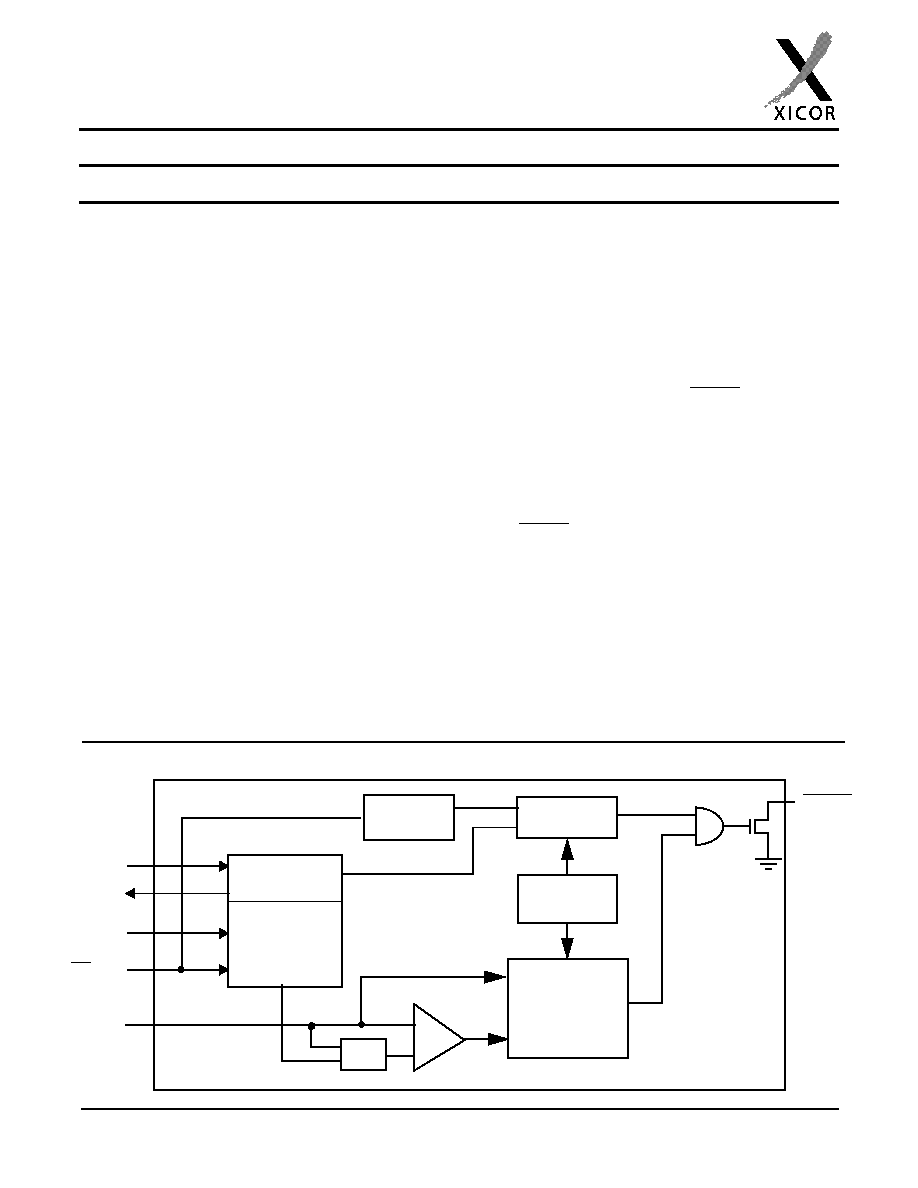
Block Diagram
DATA
REGISTER
COMMAND
DECODE &
CONTROL
LOGIC
SI
SO
SCK
CS/WDI
7036 FRM 01
V
CC
WATCHDOG
TRANSITION
DETECTOR
RESET &
WATCHDOG
TIMEBASE
POWER ON/
GENERATION
V
TRIP
+
-
RESET
RESET
LOW VOLTAGE
X5001
2
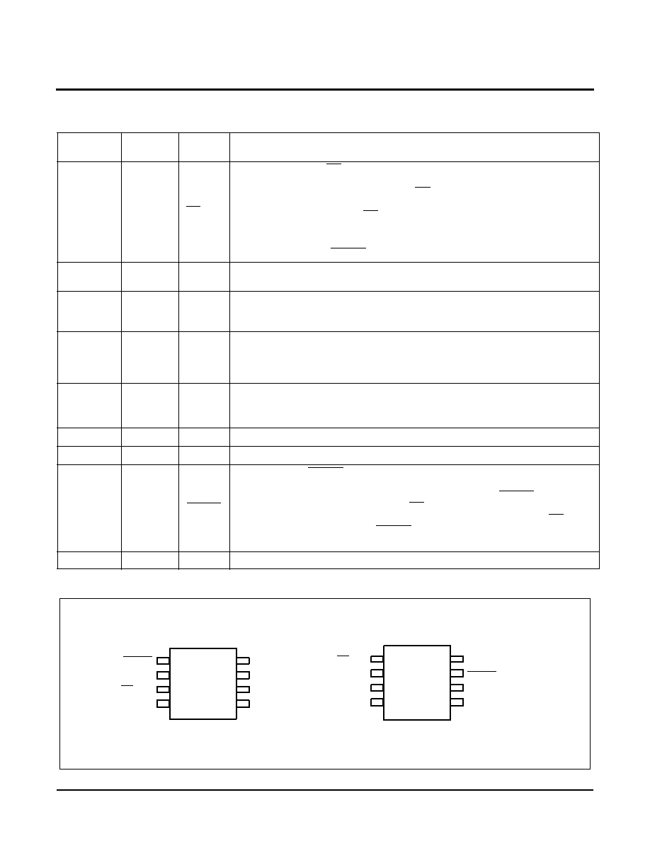
PIN DESCRIPTION
Figure 1. PIN CONFIGURATION
PIN
(SOIC/PDIP)
PIN
TSSOP
Name
Function
1
1
CS/WDI
Chip Select Input.
CS HIGH, deselects the device and the SO output pin is at
a high impedance state. Unless a nonvolatile write cycle is underway, the de-
vice will be in the standby power mode. CS LOW enables the device, placing it
in the active power mode. Prior to the start of any operation after power up, a
HIGH to LOW transition on CS is required
Watchdog Input.
A HIGH to LOW transition on the WDI pin restarts the Watch-
dog timer. The absence of a HIGH to LOW transition within the watchdog time-
out period results in RESET/RESET going active.
2
2
SO
Serial Output.
SO is a push/pull serial data output pin. A read cycle shifts data
out on this pin. The falling edge of the serial clock (SCK) clocks the data out.
5
8
SI
Serial Input.
SI is a serial data input pin. Input all opcodes, byte addresses, and
memory data on this pin. The rising edge of the serial clock (SCK) latches the
input data. Send all opcodes (Table 1), addresses and data MSB first.
6
9
SCK
Serial Clock.
The Serial Clock controls the serial bus timing for data input and
output. The rising edge of SCK latches in the opcode, address, or watchdog
bits present on the SI pin. The falling edge of SCK changes the data output on
the SO pin.
3
6
V
PE
V
TRIP
Program Enable.
When V
PE
is LOW, the V
TRIP
point is fixed at the last
valid programmed level. To readjust the V
TRIP
level, requires that the VPE pin
be pulled to a high voltage (15-18V).
4
7
V
SS
Ground
8
14
V
CC
Supply Voltage
7
13
RESET
Reset Output
.
RESET is an active LOW, open drain output which goes active
whenever Vcc falls below the minimum Vcc sense level. It will remain active un-
til Vcc rises above the minimum Vcc sense level for 200ms. RESET goes active
if the Watchdog Timer is enabled and CS/WDI remains either HIGH or LOW
longer than the selectable Watchdog time-out period. A falling edge of CS/WDI
will reset the Watchdog Timer. RESET goes active on power up at 1V and re-
mains active for 200ms after the power supply stabilizes.
3-5,10-12
NC
No internal connections
8 Lead SOIC/PDIP
X5001
CS/WDI
SO
1
2
3
4
RESET
8
7
6
5
VCC
VSS
SCK
SI
SCK
SI
VSS
V
CC
CS/WDI
SO
1
2
3
4
8
7
6
5
8 Lead TSSOP
X5001
RESET
V
PE
V
PE

X5001
3
PRINCIPLES OF OPERATION
Power On Reset
Application of power to the X5001 activates a Power On
Reset Circuit. This circuit goes active at 1V and pulls the
RESET/RESET pin active. This signal prevents the sys-
tem microprocessor from starting to operate with insuffi-
cient voltage or prior to stabilization of the oscillator. When
Vcc exceeds the device V
TRIP
value for 200ms (nominal)
the circuit releases RESET, allowing the processor to
begin executing code.
Low voltage monitoring
During operation, the X5001 monitors the V
CC
level and
asserts RESET if supply voltage falls below a preset mini-
mum V
TRIP
. The RESET signal prevents the microproces-
sor from operating in a power fail or brownout condition.
The RESET signal remains active until the voltage drops
below 1V. It also remains active until Vcc returns and
exceeds V
TRIP
for 200ms.
watchdog timer
The Watchdog Timer circuit monitors the microprocessor
activity by monitoring the WDI input. The microprocessor
must toggle the CS/WDI pin periodically to prevent a
RESET signal. The CS/WDI pin must be toggled from
HIGH to LOW prior to the expiration of the watchdog time-
out period. The state of two nonvolatile control bits in the
Watchdog Register determine the watchdog timer period.
Vcc Threshold Reset Procedure
The X5001 is shipped with a standard Vcc threshold
(V
TRIP
) voltage. This value will not change over normal
operating and storage conditions. However, in applica-
tions where the standard V
TRIP
is not exactly right, or if
higher precision is needed in the V
TRIP
value, the X5001
threshold may be adjusted. The procedure is described
below, and requires the application of a high voltage con-
trol signal.
Setting the V
TRIP
Voltage
This procedure is used to set the V
TRIP
to a higher volt-
age value. For example, if the current V
TRIP
is 4.4V and
the new V
TRIP
is 4.6V, this procedure will directly make
the change. If the new setting is to be lower than the cur-
rent setting, then it is necessary to reset the trip point
before setting the new value.
To set the new V
TRIP
voltage, apply the desired V
TRIP
threshold voltage to the Vcc pin and tie the W
PE
pin to the
programming voltage V
P
. Then a V
TRIP
programming
command sequence is sent to the device over the SPI
interface. This V
TRIP
programming sequence consists of
pulling CS LOW, then clocking in data 03h, 00h and 01h.
This is followed by bringing CS HIGH then LOW and
clocking in data 02h, 00h, and 01h (in order) and bringing
CS HIGH. This initiates the V
TRIP
programming
sequence. V
P
is brought LOW to end the operation.
Resetting the V
TRIP
Voltage
This procedure is used to set the V
TRIP
to a "native" volt-
age level. For example, if the current V
TRIP
is 4.4V and
the new V
TRIP
must be 4.0V, then the V
TRIP
must be
reset. When V
TRIP
is reset, the new V
TRIP
is something
less than 1.7V. This procedure must be used to set the
voltage to a lower value.
To reset the V
TRIP
voltage, apply greater than 3V to the
Vcc pin and tie the W
PE
pin to the programming voltage
Vp. Then a V
TRIP
command sequence is sent to the
device over the SPI interface. This V
TRIP
programming
sequence consists of pulling CS LOW, then clocking in
data 03h, 00h and 01h. This is followed by bringing CS
HIGH then LOW and clocking in data 02h, 00h, and 03h
(in order) and bringing CS HIGH. This initiates the V
TRIP
programming sequence. V
P
is brought LOW to end the
operation.
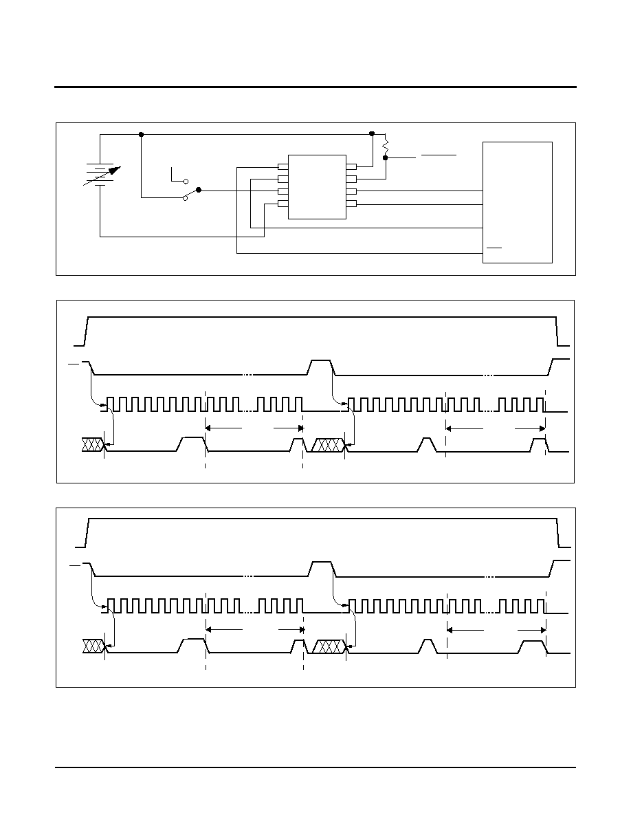
X5001
4
Figure 2. Sample V
TRIP
Reset Circuit
Figure 3. Set V
TRIP
Level Sequence (Vcc=desired V
TRIP
value. )
Figure 4. Reset V
TRIP
Level Sequence (Vcc > 3V. )
1
2
3
4
8
7
6
5
X5001
V
TRIP
Adj.
V
P
RESET
4.7K
SI
SO
CS
SCK
uC
Adjust
Run
0
1
2 3 4
5 6
7 8
9 10
SCK
SI
CS
20 21 22 23
16 BITS
0001h
03h
0
1
2 3 4
5 6
7 8
9 10
20 21 22 23
16 BITS
0001h
02h
V
PE
V
PE
= 15-18V
0
1
2 3 4
5 6
7 8
9 10
SCK
SI
CS
20 21 22 23
16 BITS
0001h
03h
0
1
2 3 4
5 6
7 8
9 10
20 21 22 23
16 BITS
0003h
02h
V
PE
V
PE
= 15-18V
16 BITS
X5001
5
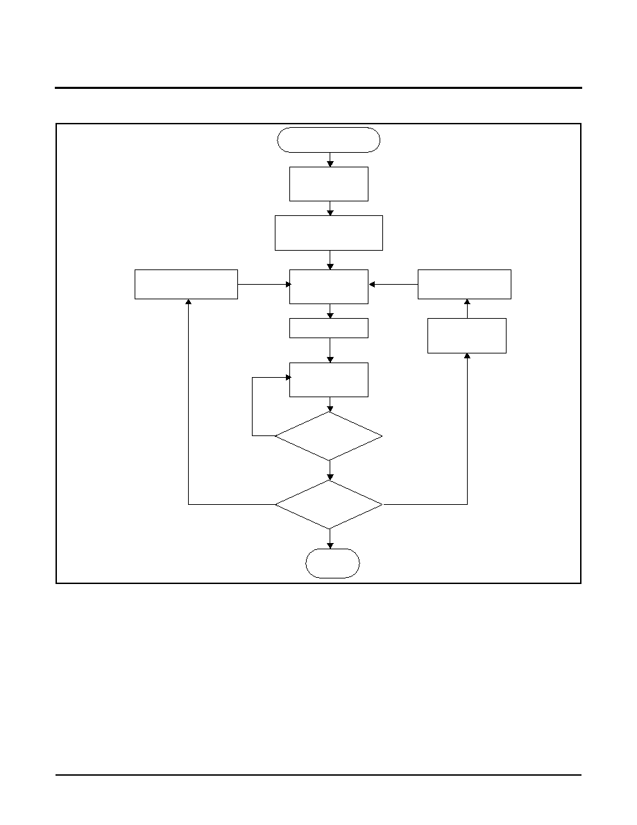
Figure 5. Vtrip Programming Sequence
Vtrip Programming
Apply 5V to Vcc
Decrement Vcc
RESET pin
goes active?
Measured Vtrip
-
Desired Vtrip
DONE
Execute
Sequence
Reset Vtrip
Set Vcc = Vcc applied =
Desired Vtrip
Execute
Sequence
Set Vtrip
New Vcc applied =
Old Vcc applied
+
Error
(Vcc = Vcc - 50mV)
Execute
Sequence
Reset Vtrip
New Vcc applied =
Old Vcc applied
-
Error
Error < 0
Error = 0
YES
NO
Error > 0

X5001
6
spi Interface
The device is designed to interface directly with the syn-
chronous Serial Peripheral Interface (SPI) of many popu-
lar microcontroller families.
The device monitors the CS/WDI line and asserts RESET
output if there is no activity within user selctable time-out
period. The device also monitors the Vcc supply and
asserts the RESET if Vcc falls below a preset minimum
(V
TRIP
). The device contains an 8-bit Watchdog Timer
Register to control the watchdog time-out period. The cur-
rent settings are accessed via the SI and SO pins.
All instructions (Table 1) and data are transferred MSB
first. Data input on the SI line is latched on the first rising
edge of SCK after CS goes LOW. Data is output on the
SO line by the falling edge of SCK. SCK is static, allowing
the user to stop the clock and then start it again to resume
operations where left off.
Watchdog Timer Register
Watchdog Timer Control Bits
The Watchdog Timer Control bits, WD
0
and WD
1
, select
the Watchdog Time-out Period. These nonvolatile bits are
programmed with the Set Watchdog Timer (SWDT)
instruction.
Write Watchdog Register Operation
Changing the Watchdog Timer Register is a two step pro-
cess. First, the change must be enabled with by setting
the Watchdog Change Latch (see below). This instruction
is followed by the Set Watchdog Timer (SWDT) instruc-
tion, which includes the data to be written (Figure 5). Data
bits 3 and 4 contain the Watchdog settings and data bits
0, 1, 2, 5, 6 and 7 must be "0" .
Watchdog Change Latch
The Watchdog Change Latch must be SET before a Write
Watchdog Timer Operation is initiated. The Enable
Watchdog Change (EWDC) instruction will set the latch
and the Disable Watchdog Change (DWDC) instruction
will reset the latch (See Figure 2.) This latch is automati-
cally reset upon a power-up condition and after the com-
pletion of a valid nonvolatile write cycle.
Read Watchdog Timer Register Operation
If there is not a nonvolatile write in progress, the Read
Watchdog Timer instruction returns the setting of the
watchdog timer control bits. The other bits are reserved
and will return '0' when read. See Figure 3.
If a nonvolatile write is in progress, the Read Watchdog
Timer Register Instruction returns a HIGH on SO. When
the nonvolatile write cycle is completed, a seperate Read
Watchdog Timer instruction should be used to determine
the current status of the Watchdog control bits.
RESET Operation
The RESET (X5001) output is designed to go LOW
whenever V
CC
has dropped below the minimum trip point
and/or the Watchdog timer has reached its programmable
time-out limit.
The RESET output is an open drain output and requires a
pull up resistor.
Operational Notes
The device powers-up in the following state:
∑ The device is in the low power standby state.
∑ A HIGH to LOW transition on CS is required to enter an
active state and receive an instruction.
∑ SO pin is high impedance.
∑ The Watchdog Change Latch is reset.
∑ The RESET Signal is active for t
PURST
.
Data Protection
The following circuitry has been included to prevent inad-
vertent writes:
∑ A EWDC instruction must be issued to enable a change
to the watchdog timeout setting.
∑ CS must come HIGH at the proper clock count in order
to implement the requested changes to the watchdog
timeout setting.
7
6
5
4
3
2
1
0
0
0
0
WD
1
WD
0
0
0
0
Watchdog Control Bits
Watchdog Time-out
(Typical)
WD1
WD0
0
0
1.4 Seconds
0
1
600 Milliseconds
1
0
200 Milliseconds
1
1
Disabled
X5001
7
Table 1. Instruction Set Definition
Notes: Instructions are shown with MSB in leftmost position. Instructions are transferred MSB first.
7038 FRM T03
Figure 1. Read Watchdog Timer setting
Figure 2. Enable Watchdog Change/Disable Watchdog Change Sequence
Instruction Format
Instruction Name and Operation
0000 0110
EWDC: Enable Watchdog Change Operation
0000 0100
DWDC: Disable Watchdog Change Operation
0000 0001
SWDT: Set Watchdog Timer control bits:
Instruction followed by contents of register: 000(WD
1
) (WD
0
)000
See Watchdog Timer Settings and Figure 3.
0000 0101
RWDT: Read Watchdog Timer control bits
0
1
2
3
4
5
6
7
CS
SCK
SI
SO
RWDT
INSTRUCTION
...
...
...
W
D
0
W
D
1
0
1
2
3
4
5
6
7
CS
SI
SCK
HIGH IMPEDANCE
SO
INSTRUCTION
(1 BYTE)
X5001
8
Figure 3. Write Watchdog Timer Sequence
Figure 4. Read Nonvolatile Status (Option 1) (Used to determine end of Watchdog Timer store operation)
Figure 5. Read Nonvolatile Status (Option 2) (Used to determine end of Watchdog Timer store operation)
0
1
2
3
4
5
6
7
8
9
CS
SCK
SI
SO
HIGH IMPEDANCE
INSTRUCTION
10
11
12
13
14
15
DATA BYTE
6
5
4
3
W
D
1
W
D
0
0
1
2
3
4
5
6
7
CS
SCK
SI
SO
NONVOLATILE WRITE IN PROGRESS
RWDT
INSTRUCTION
SO HIGH During 1st bit while
in the Nonvolatile write cycle
0
1
2
3
4
5
6
7
CS
SCK
SI
SO
NONVOLATILE WRITE IN PROGRESS
RWDT
INSTRUCTION
SO HIGH During
Nonvolatile write cycle
X5001
9
D.C. OPERATING CHARACTERISTICS (Over the recommended operating conditions unless otherwise specified.)
POWER-UP TIMING
CAPACITANCE T
A
= +25∞C, f = 1MHz, V
CC
= 5V.
Notes:
(1) V
IL
min. and V
IH
max. are for reference only and are not tested.
(2) This parameter is periodically sampled and not 100% tested.
Symbol
Parameter
Limits
Units
Test Conditions
Min.
Typ.
Max.
I
CC1
V
CC
Write Current (Active)
5
mA
SCK = V
CC
x 0.1/V
CC
x 0.9 @ 5MHz,
SO = Open
I
CC2
V
CC
Read Current (Active)
0.4
mA
SCK = V
CC
x 0.1/V
CC
x 0.9 @ 5MHz,
SO = Open
I
SB1
V
CC
Standby Current WDT=OFF
1
µA
CS = V
CC
, V
IN
= V
SS
or V
CC
, V
CC
= 5.5V
I
SB2
V
CC
Standby Current WDT=ON
50
µA
CS = V
CC
, V
IN
= V
SS
or V
CC
, V
CC
= 5.5V
I
SB3
V
CC
Standby Current WDT=ON
20
µA
CS = V
CC
, V
IN
= V
SS
or V
CC
, V
CC
=3.6V
I
LI
Input Leakage Current
0.1
10
µA
V
IN
= V
SS
to V
CC
I
LO
Output Leakage Current
0.1
10
µA
V
OUT
= V
SS
to V
CC
V
IL
(1)
Input LOW Voltage
≠0.5
V
CC
x0.3
V
V
IH
(1)
Input HIGH Voltage
V
CC
x0.7
V
CC
+0.5
V
V
OL1
Output LOW Voltage
0.4
V
V
CC
> 3.3V, I
OL
= 2.1mA
V
OL2
Output LOW Voltage
0.4
V
2V < V
CC
< 3.3V, I
OL
= 1mA
V
OL3
Output LOW Voltage
0.4
V
V
CC
2V, I
OL
= 0.5mA
V
OH1
Output HIGH Voltage
V
CC
≠0.8
V
V
CC
> 3.3V, I
OH
= ≠1.0mA
V
OH2
Output HIGH Voltage
V
CC
≠0.4
V
2V < V
CC
3.3V, I
OH
= ≠0.4mA
V
OH3
Output HIGH Voltage
V
CC
≠0.2
V
V
CC
2V, I
OH
= ≠0.25mA
V
OLRS
Reset Output LOW Voltage
0.4
V
I
OL
= 1mA
Symbol
Parameter
Min.
Max.
Units
t
PUR
(2)
Power-up to Read Operation
1
ms
t
PUW
(2)
Power-up to Write Operation
5
ms
Symbol
Test
Max.
Units
Conditions
C
OUT
(2)
Output Capacitance (SO, RESET)
8
pF
V
OUT
= 0V
C
IN
(2)
Input Capacitance (SCK, SI, CS)
6
pF
V
IN
= 0V
ABSOLUTE MAXIMUM RATINGS*
Temperature under Bias ........................≠65∞C to +135∞C
Storage Temperature .............................≠65∞C to +150∞C
Voltage on any Pin with Respect to V
SS
....... ≠1.0V to +7V
D.C. Output Current ....................................................5mA
Lead Temperature (Soldering, 10 seconds)............ 300∞C
RECOMMENDED OPERATING CONDITIONS
7036 FRM T07
*COMMENT
Stresses above those listed under "Absolute Maximum
Ratings" may cause permanent damage to the device.
This is a stress rating only and the functional operation of
the device at these or any other conditions above those
listed in the operational sections of this specification is not
implied. Exposure to absolute maximum rating conditions
for extended periods may affect device reliability.
PT= Package, Temperature
Temp
Min.
Max.
Commercial
0∞C
+70∞C
Voltage Option
Supply Voltage Limits
≠1.8
1.8V to 3.6V
≠2.7 or -2.7A
2.7V to 5.5V
≠4.5 or -4.5A
4.5V to 5.5V
X5001
10
A.C. CHARACTERISTICS (Over recommended operating conditions, unless otherwise specified)
Data Input Timing
Data Output Timing
Notes:
(3) This parameter is periodically sampled and not 100% tested.
(4) t
WC
is the time from the rising edge of CS after a valid write sequence has been sent to the end of the self-timed internal
nonvolatile write cycle.
1.8V≠3.6V
2.7V≠5.5V
Symbol
Parameter
Min. Max.
Min. Max.
Units
f
SCK
Clock Frequency
0
1
0
2
MHz
t
CYC
Cycle Time
1000
500
ns
t
LEAD
CS Lead Time
400
200
ns
t
LAG
CS Lag Time
400
200
ns
t
WH
Clock HIGH Time
400
200
ns
t
WL
Clock LOW Time
400
200
ns
t
SU
Data Setup Time
100
50
ns
t
H
Data Hold Time
100
50
ns
t
RI
(3)
Input Rise Time
2
2
µs
t
FI
(3)
Input Fall Time
2
2
µs
t
CS
CS Deselect Time
250
150
ns
t
WC
(4)
Write Cycle Time
10
10
ms
1.8V≠3.6V
2.7V≠5.5V
Symbol
Parameter
Min.
Max.
Min.
Max.
Units
f
SCK
Clock Frequency
0
1
0
2
MHz
t
DIS
Output Disable Time
400
200
ns
t
V
Output Valid from Clock Low
400
200
ns
t
HO
Output Hold Time
0
0
ns
t
RO
(3)
Output Rise Time
300
150
ns
t
FO
(3)
Output Fall Time
300
150
ns
Figure 1. EQUIVALENT A.C. LOAD CIRCUIT
A.C. TEST CONDITIONS
3V
OUTPUT
100pF
5V
3.3K
RESET
30pF
1.64K
1.64
K
Input Pulse Levels
V
CC
x 0.1 to V
CC
x 0.9
Input Rise and Fall Times
10ns
Input and Output Timing Level
V
CC
x0.5
X5001
11
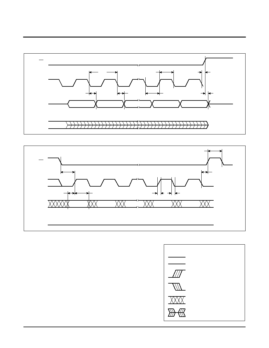
Figure 1. Data Output Timing
Figure 2. Data Input Timing
SCK
CS
SO
SI
MSB OUT
MSB≠1 OUT
LSB OUT
ADDR
LSB IN
t
CYC
t
V
t
HO
t
WL
t
WH
t
DIS
t
LAG
SCK
CS
SI
SO
MSB IN
t
SU
t
RI
t
LAG
t
LEAD
t
H
LSB IN
t
CS
t
FI
HIGH IMPEDANCE
WAVEFORM
INPUTS
OUTPUTS
Must be
steady
Will be
steady
May change
from LOW
to HIGH
Will change
from LOW
to HIGH
May change
from HIGH
to LOW
Will change
from HIGH
to LOW
Don't Care:
Changes
Allowed
Changing:
State Not
Known
N/A
Center Line
is High
Impedance
Figure 1. Symbol Table
X5001
12
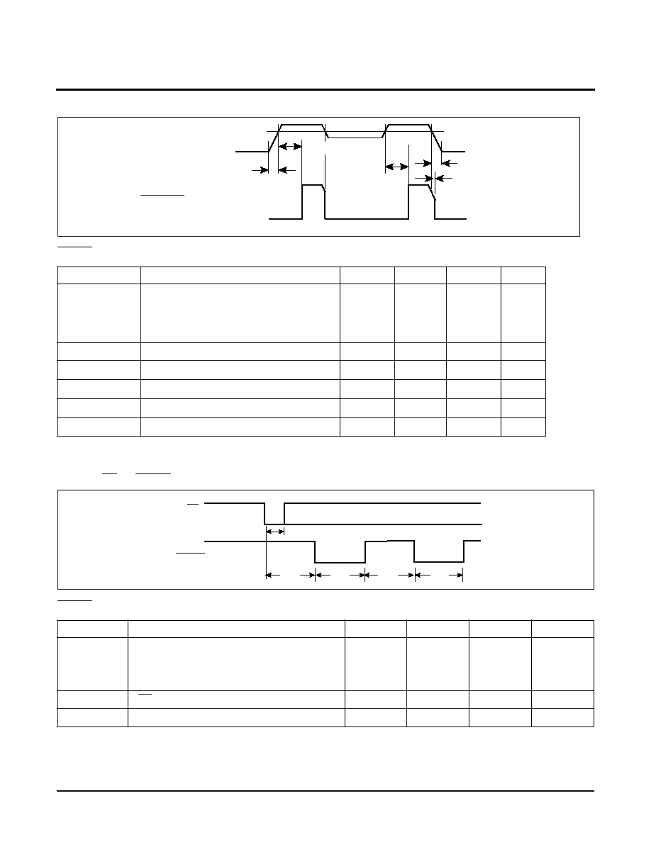
Figure 1. Power-Up and Power-Down Timing
RESET Output Timing
Notes:
(5) This parameter is periodically sampled and not 100% tested.
PT = Package, Temperature
Figure 2. CS vs. RESET Timing
RESET Output Timing
Symbol
Parameter
Min.
Typ.
Max.
Units
V
TRIP
Reset Trip Point Voltage, X5001PT-4.5A
Reset Trip Point Voltage, X5001PT-4.5
Reset Trip Point Voltage, X5001PT-2.7A
Reset Trip Point Voltage, X5001PT-2.7
Reset Trip Point Voltage, X5001PT-1.8
4.50
4.25
2.85
2.55
1.70
4.63
4.38
2.92
2.63
1.75
4.75
4.50
3.00
2.70
1.80
V
t
PURST
Power-up Reset Timeout
100
200
280
ms
t
RPD
(5)
V
CC
Detect to Reset/Output
500
ns
t
F
(5)
V
CC
Fall Time
0.1
ns
t
R
(5)
V
CC
Rise Time
0.1
ns
V
RVALID
Reset Valid V
CC
1
V
Symbol
Parameter
Min.
Typ.
Max.
Units
t
WDO
Watchdog Timeout Period,
WD
1
= 1, WD
0
= 0
WD
1
= 0, WD
0
= 1
WD
1
= 0, WD
0
= 0
100
450
1
200
600
1.4
300
800
2
ms
ms
sec
t
CST
CS Pulse Width to Reset the Watchdog
400
ns
t
RST
Reset Timeout
100
200
300
ms
VCC
t
PURST
t
PURST
t
R
t
F
t
RPD
RESET (X5001)
0 Volts
V
TRIP
V
TRIP
CS
t
CST
RESET
t
WDO
t
RST
t
WDO
t
RST

X5001
13
V
TRIP
Programming Timing Diagram
SCK
SI
CS
0001h or
02h
Vcc
(
V
TRIP
)
V
PE
t
TSU
t
THD
t
VPH
t
VPS
V
P
V
TRIP
t
RP
t
VPO
t
PCS
0003h
0001h
03h

X5001
14
V
TRIP
Programming Parameters
Parameter
Description
Min
Max
Units
t
VPS
V
TRIP
Program Enable Voltage Setup time
1
µ
s
t
VPH
V
TRIP
Program Enable Voltage Hold time
1
µ
s
t
PCS
V
TRIP
Programming CS inactive time
1
µ
s
t
TSU
V
TRIP
Setup time
1
µ
s
t
THD
V
TRIP
Hold (stable) time
10
ms
t
WC
V
TRIP
Write Cycle Time
10
ms
t
VPO
V
TRIP
Program Enable Voltage Off time
(Between successive adjustments)
0
us
t
RP
V
TRIP
Program Recovery Period
(Between successive adjustments)
10
ms
V
P
Programming Voltage
15
18
V
V
TRAN
V
TRIP
Programmed Voltage Range
1.7
5.0
V
V
ta1
Initial V
TRIP
Program Voltage accuracy
(Vcc applied - V
TRIP
) (Programmed at 25
o
C.)
-0.1
+0.4
V
V
ta2
Subsequent V
TRIP
Program Voltage accuracy
[(Vcc applied - V
ta1
) - V
TRIP
. Programmed at 25
o
C.)
-25
+25
mV
V
tr
V
TRIP
Program Voltage repeatability
(Successive program operations. Programmed at 25
o
C.)
-25
+25
mV
V
tv
V
TRIP
Program variation after programming (0-75
o
C).
(Programmed at 25
o
C.)
-25
+25
mV
V
TRIP
Programming parameters are periodically sampled and are not 100% Tested.
X5001
15
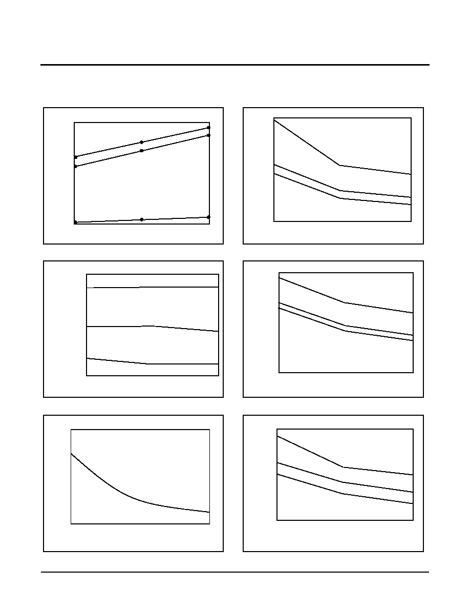
Watchdog Timer On (Vcc = 5V)
Watchdog Timer On (Vcc = 3V)
Watchdog Timer Off (Vcc = 3V, 5V)
≠40C
25C
90C
Temp (c)
Isb (uA)
Vcc Supply Current vs. Temperature (I
SB
)
t
WDO
vs. Voltage/Temperature (WD1,0=1,1)
V
TRIP
vs. Temperature (programmed at 25∞C)
t
WDO
vs. Voltage/Temperature (WD1,0=1,0)
t
PURST
vs. Temperature
t
WDO
vs. Voltage/Temperature (WD1,0 0=0,1)
1.85
1.80
1.75
1.70
1.65
1.60
1.55
1.50
1.45
1.40
1.7
3.1
4.5
90∞C
25∞C
≠40∞C
Reset (seconds)
Voltage
5.025
5.000
4.975
3.525
3.500
3.475
2.525
2.500
2.475
0
25
85
Voltage
Temperature
Vtrip=5V
Vtrip=3.5V
Vtrip=2.5V
0.85
0.80
0.75
0.70
0.65
0.60
1.7
4.5
Reset (seconds)
Voltage
3.1
90∞C
25∞C
≠40∞C
275
270
265
260
255
250
245
240
235
≠40
25
90
Degrees ∞C
280
Time (ms)
90∞C
25∞C
≠40∞C
0.28
0.27
0.26
0.25
0.24
0.23
0.22
0.21
0.20
0.29
Reset (seconds)
Voltage
1.7
3.1
4.5
14
11
17
15
20
18
0.35
0.55
1.0
0.30
X5001
16
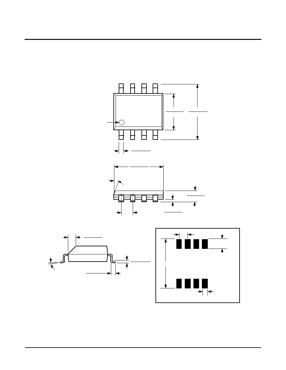
0.150 (3.80)
0.158 (4.00)
0.228 (5.80)
0.244 (6.20)
0.014 (0.35)
0.019 (0.49)
PIN 1
PIN 1 INDEX
0.010 (0.25)
0.020 (0.50)
0.050 (1.27)
0.188 (4.78)
0.197 (5.00)
0.004 (0.19)
0.010 (0.25)
0.053 (1.35)
0.069 (1.75)
(4X) 7
0.016 (0.410)
0.037 (0.937)
0.0075 (0.19)
0.010 (0.25)
0
≠ 8
X 45
8-LEAD PLASTIC SMALL OUTLINE GULL WING PACKAGE TYPE S
NOTE: ALL DIMENSIONS IN INCHES (IN PARENTHESES IN MILLIMETERS)
0.250"
0.050" TYPICAL
0.050"
TYPICAL
0.030"
TYPICAL
8 PLACES
FOOTPRINT
X5001
17
NOTE:
ALL DIMENSIONS IN INCHES (IN PARENTHESES IN MILLIMETERS)
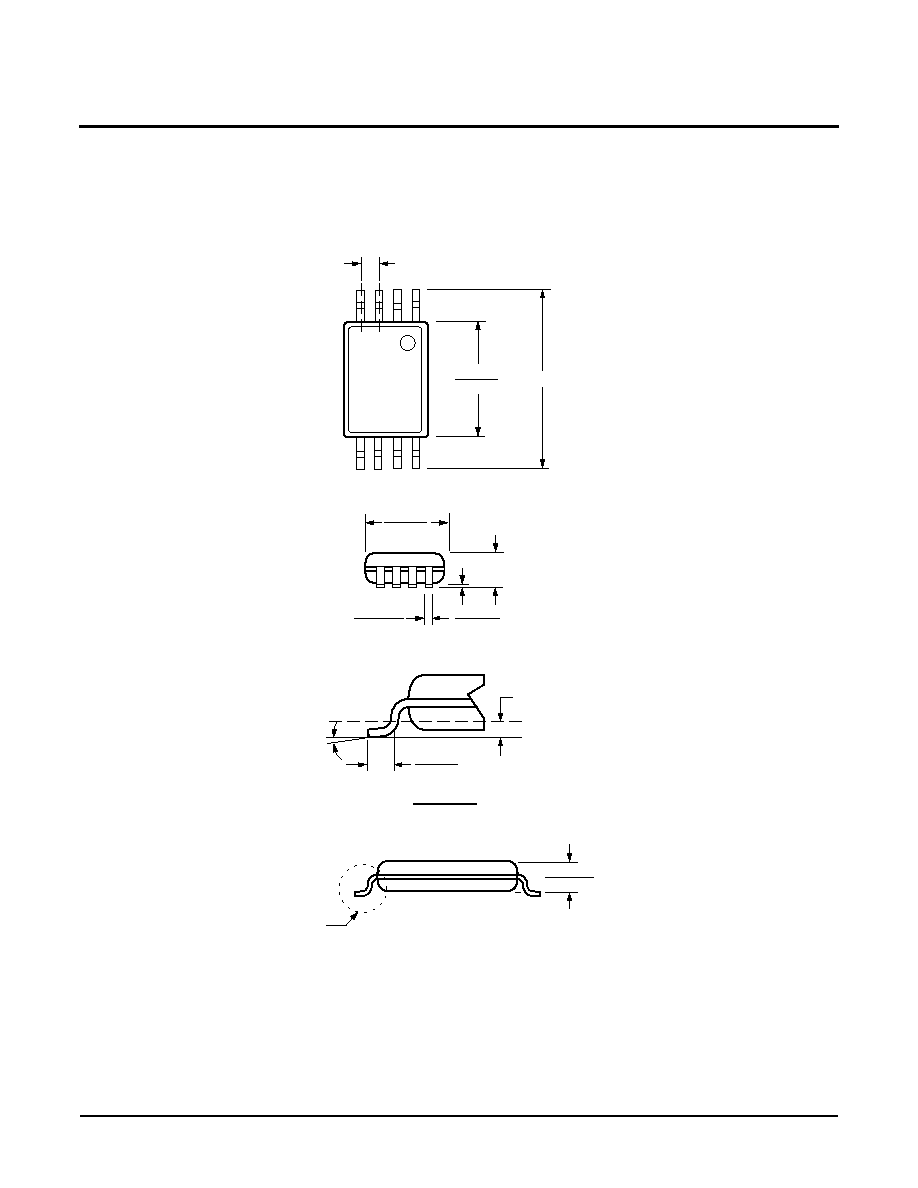
8-LEAD PLASTIC, TSSOP, PACKAGE TYPE V
See Detail "A"
.031 (.80)
.041 (1.05)
.169 (4.3)
.177 (4.5)
.252 (6.4) BSC
.025 (.65) BSC
.114 (2.9)
.122 (3.1)
.002 (.05)
.006 (.15)
.047 (1.20)
.0075 (.19)
.0118 (.30)
0
≠ 8
.010 (.25)
.019 (.50)
.029 (.75)
Gage Plane
Seating Plane
Detail A (20X)
X5001
18
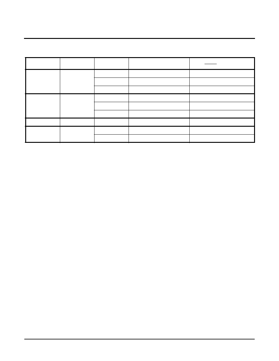
Ordering Information
Vcc Range
Vtrip Range
Package
Operating
Temperature Range
PART NUMBER
RESET (Active LOW)
4.5-5.5V
4.5.4.75
8 pin PDIP
0
o
C - 70
o
C
X5001P-4.5A
8L SOIC
0
o
C - 70
o
C
X5001S8-4.5A
8L TSSOP
0
o
C - 70
o
C
X5001V8-4.5A
4.5-5.5V
4.25.4.5
8 pin PDIP
0
o
C - 70
o
C
X5001P
8L SOIC
0
o
C - 70
o
C
X5001S8
8L TSSOP
0
o
C - 70
o
C
X5001V8
2.7-5.5V
2.85-3.0
8L SOIC
0
o
C - 70
o
C
X5001S8-2.7A
2.7-5.5V
2.55-2.7
8L SOIC
0
o
C - 70
o
C
X5001S8-2.7
8L TSSOP
0
o
C - 70
o
C
X5001V8-2.7

X5001
19
Part Mark Information
8-Lead TSSOP
501AG = 1.8 to 3.6V, 0 to +70∞C, V
TRIP
=1.7-1.8V
YWW
XXXXX
501AH = 1.8 to 3.6V, -40 to +85∞C, V
TRIP
=1.7-1.8V
501F = 2.7 to 5.5V, 0 to +70∞C, V
TRIP
=2.55-2.7V
501G = 2.7 to 5.5V, -40 to +85∞C, V
TRIP
=2.55-2.7V
501 = 4.5 to 5.5V, 0 to +70∞C, V
TRIP
=4.25-4.5V
501I = 4.5 to 5.5V, -40 to +85∞C, V
TRIP
=4.25-4.5V
8-Lead SOIC
X5001
YWW XX
AG = 1.8 to 3.6V, 0 to +70∞C, V
TRIP
=1.7-1.8V
AH = 1.8 to 3.6V, -40 to +85∞C, V
TRIP
=1.7-1.8V
F = 2.7 to 5.5V, 0 to +70∞C, V
TRIP
=2.55-2.7V
G = 2.7 to 5.5V, -40 to +85∞C, V
TRIP
=2.55-2.7V
I = 4.5 to 5.5V, -40 to +85∞C, V
TRIP
=4.25-4.5V
501AN = 2.7 to 5.5V, 0 to +70∞C, V
TRIP
=2.85-3.0V
501AP = 2.7 to 5.5V, -40 to +85∞C, V
TRIP
=2.85-3.0V
501AL = 4.5 to 5.5V, 0 to +70∞C, V
TRIP
=4.5-4.75V
501AM = 4.5 to 5.5V, -40 to +85∞C, V
TRIP
=4.5-4.75V
AN = 2.7 to 5.5V, 0 to +70∞C, V
TRIP
=2.85-3.0V
AP = 2.7 to 5.5V, -40 to +85∞C, V
TRIP
=2.85-3.0V
AL = 4.5 to 5.5V, 0 to +70∞C, V
TRIP
=4.5-4.75V
AM = 4.5 to 5.5V, -40 to +85∞C, V
TRIP
=4.5-4.75V
Blank = 4.5 to 5.5V, 0 to +70∞C, V
TRIP
=4.25-4.5V
YWW = year/work week device is packaged.
LIMITED WARRANTY
Devices sold by Xicor, Inc. are covered by the warranty and patent indemnification provisions appearing in its Terms of Sale only. Xicor, Inc. makes no
warranty, express, statutory, implied, or by description regarding the information set forth herein or regarding the freedom of the described devices
from patent infringement. Xicor, Inc. makes no warranty of merchantability or fitness for any purpose. Xicor, Inc. reserves the right to discontinue
production and change specifications and prices at any time and without notice.
Xicor, Inc. assumes no responsibility for the use of any circuitry other than circuitry embodied in a Xicor, Inc. product. No other circuits, patents,
licenses are implied.
U.S. PATENTS
Xicor products are covered by one or more of the following U.S. Patents: 4,263,664; 4,274,012; 4,300,212; 4,314,265; 4,326,134; 4,393,481;
4,404,475; 4,450,402; 4,486,769; 4,488,060; 4,520,461; 4,533,846; 4,599,706; 4,617,652; 4,668,932; 4,752,912; 4,829, 482; 4,874, 967; 4,883, 976.
Foreign patents and additional patents pending.
LIFE RELATED POLICY
In situations where semiconductor component failure may endanger life, system designers using this product should design the system with appro-
priate error detection and correction, redundancy and back-up features to prevent such an occurence.
Xicor's products are not authorized for use in critical components in life support devices or systems.
1. Life support devices or systems are devices or systems which, (a) are intended for surgical implant into the body, or (b) support or sustain life, and
whose failure to perform, when properly used in accordance with instructions for use provided in the labeling, can be reasonably expected to result
in a significant injury to the user.
2. A critical component is any component of a life support device or system whose failure to perform can be reasonably expected to cause the failure
of the life support device or system, or to affect its safety or effectiveness.