 | –≠–ª–µ–∫—Ç—Ä–æ–Ω–Ω—ã–π –∫–æ–º–ø–æ–Ω–µ–Ω—Ç: X5563 | –°–∫–∞—á–∞—Ç—å:  PDF PDF  ZIP ZIP |
REV 1.8 9/30/02
Characteristics subject to change without notice.
1 of 18
www.xicor.com
Preliminary Information
X5563
CPU Supervisor with 256Kbit SPI EEPROM
FEATURES
∑ Low V
CC
detection and reset assertion
--Four standard reset threshold voltages
--Re-program low V
CC
reset threshold voltage
using special programming sequence
--Reset signal valid to V
CC
= 1V
∑ Selectable POR time (150ms or 800ms)
∑ Selectable watchdog time
--(0.15s, 0.4s, 0.8s, off)
∑ Debounced Manual Reset Input
∑ Low power consumption
--<90µA max standby current, watchdog on
--<50µA max standby current, watchdog off
--<1.5mA max active current during read
∑ 256Kbits of EEPROM
∑ Built-in inadvertent write protection
--Power-up/power-down protection circuitry
--Protect 0, 1/4, 1/2 or all of EEPROM array with
programmable Block Lock
TM
protection
--In circuit programmable ROM mode
∑ 10MHz SPI interface modes (0,0 & 1,1)
∑ Minimize EEPROM programming time
--64 byte page write mode
--Self-timed write cycle
--5ms write cycle time (typical)
∑ 2.7V to 5.5V power supply operation
∑ Available packages
--8-lead SOIC
DESCRIPTION
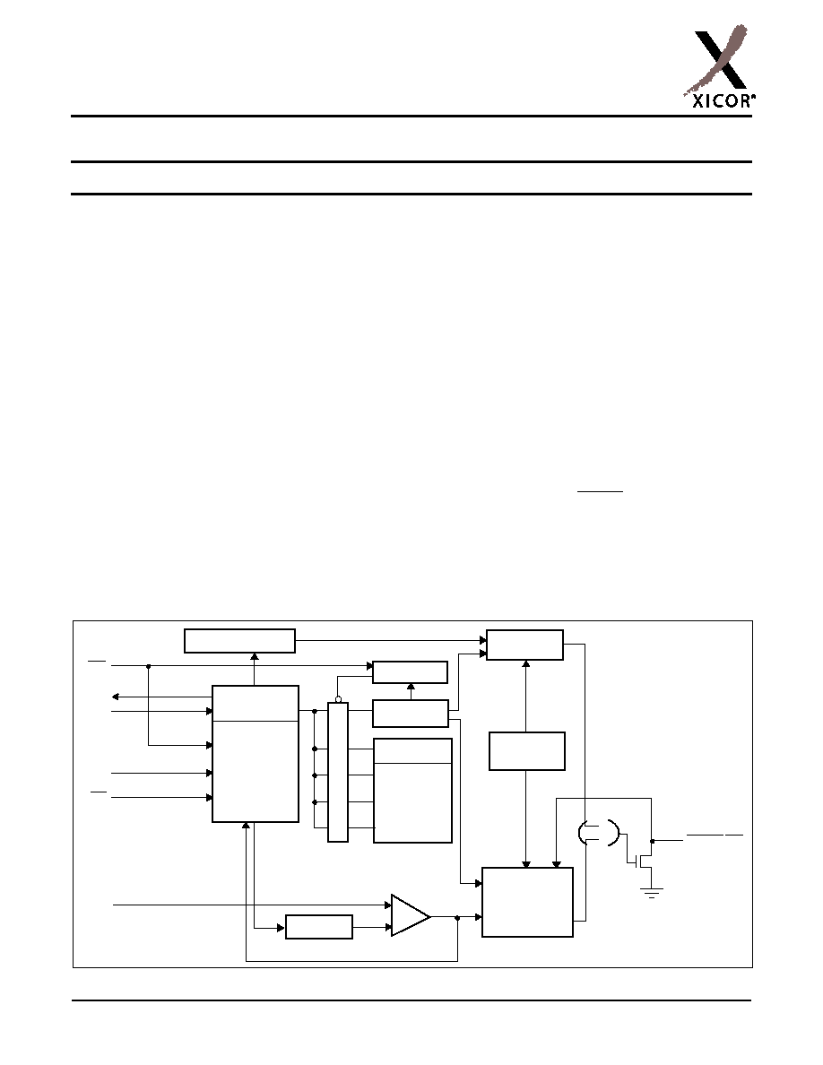
These devices combines power-on reset control,
watchdog timer, supply voltage supervision, manual
reset, block lock protect and serial EEPROM in one
package. This combination lowers system cost, reduces
board space requirements, and increases reliability.
Applying power to the device activates the power on
reset circuit which holds RESET active for a selected
period of time. This allows the power supply and oscil-
lator to stabilize before the processor can execute
code.
BLOCK DIAGRAM
Watchdog
Timer Reset
Data
Register
Command
Decode, Test &
Control
Logic
SI
SO
SCK
CS
V
CC
Reset &
Watchdog
Timebase
Power on,
Generation
V
CC
Monitor
+
-
Reset
Low Voltage
Status
Register
Protect Logic
EEPROM Array
Watchdog Transition
Detector
WP
512 X 512
X-Decoder
V
TRIP
Logic
RESET/MR
X5563 ≠ Preliminary Information
Characteristics subject to change without notice.
2 of 18
REV 1.8 9/30/02
www.xicor.com
The Watchdog Timer provides an independent protection
mechanism for microcontrollers. When the micro-
controller fails to restart a timer within a selectable time
out interval, the device activates the RESET signal. The
user selects the interval from three preset values.
Once selected, the interval does not change, even
after cycling the power.
The device's low V
CC
detection circuitry protects the
user's system from low voltage conditions, resetting
the system when V
CC
falls below the minimum V
CC
trip
point (V
TRIP
). RESET is asserted until V
CC
returns to
proper operating level and stabilizes. Xicor's unique cir-
cuits allow the threshold for either voltage monitor to
be reprogrammed to meet special needs or to fine-tune
the threshold for applications requiring higher preci-
sion.
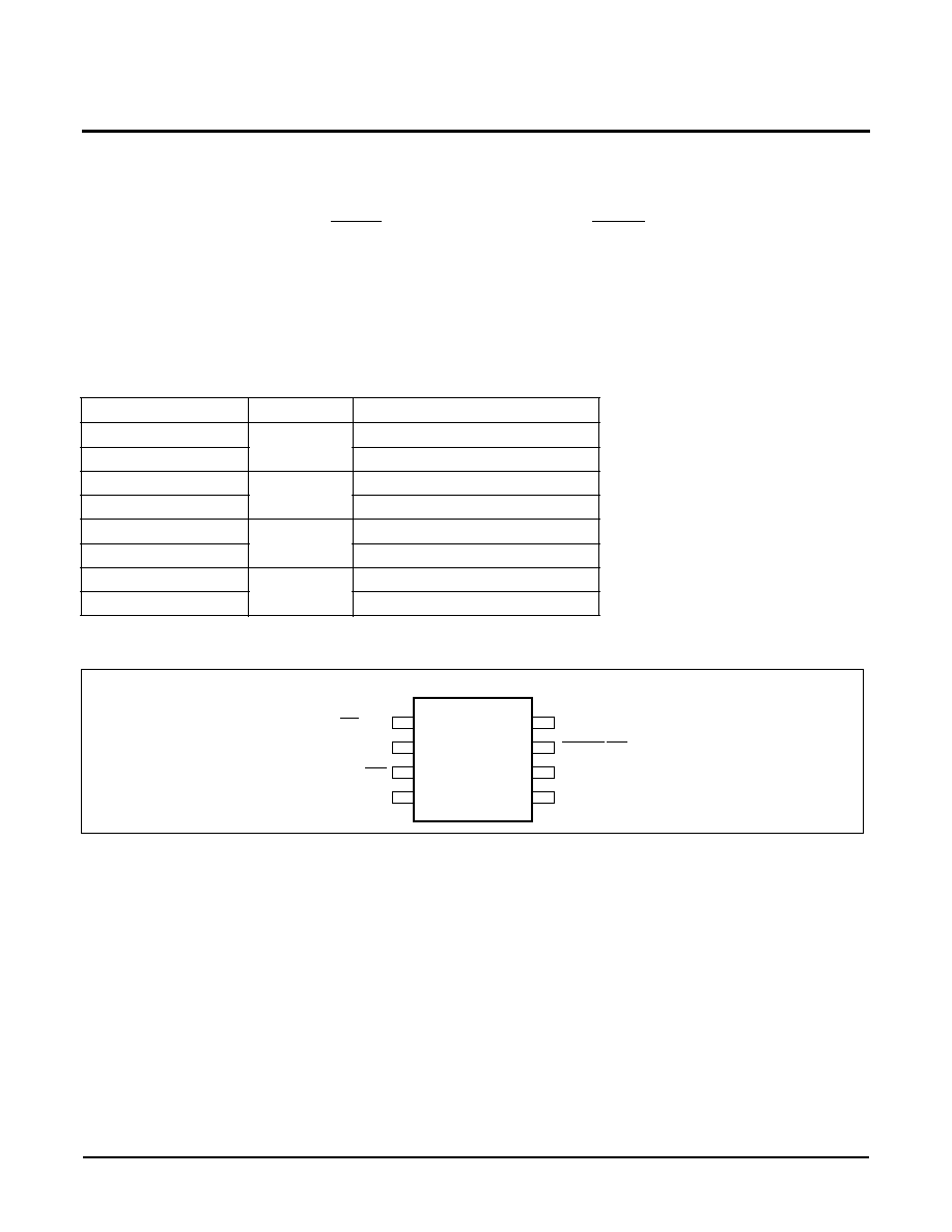
Ordering Information
PIN CONFIGURATION
Part Number
Vtrip1
Temperature Range
X5563S8-4.5A
4.63
0∞C≠70∞C
X5563S8I-4.5A
-40∞C≠85∞C
X5563S8
4.38
0∞C≠70∞C
X5563S8I
-40∞C≠85∞C
X5563S8-2.7A
2.93
0∞C≠70∞C
X5563S8I-2.7A
-40∞C≠85∞C
X5563S8-2.7
2.63
0∞C≠70∞C
X5563S8I-2.7
-40∞C≠85∞C
8-Pin SOIC
CS/WDI
SO
1
2
3
4
RESET/MR
V
CC
8
7
6
5
WP
V
SS
SCK
SI

X5563 ≠ Preliminary Information
Characteristics subject to change without notice.
3 of 18
REV 1.8 9/30/02
www.xicor.com
PIN DEFINITIONS
Pin
Name
Function
1
CS/WDI
Chip Select Input.
CS HIGH, deselects the device and the SO output pin is at a high impedance
state. Unless a nonvolatile write cycle is underway, the device will be in the standby power mode.
CS LOW enables the device, placing it in the active power mode. Prior to the start of any opera-
tion after power up, a HIGH to LOW transition on CS is required.
Watchdog Input.
A HIGH to LOW transition on the WDI pin restarts the Watchdog timer. The
absence of a HIGH to LOW transition within the watchdog time out period results in RESET going
active.
2
SO
Serial Output.
SO is a push/pull serial data output pin. A read cycle shifts data out on this pin. The
falling edge of the serial clock (SCK) clocks the data out.
3
WP
Write Protect.
The WP pin works in conjunction with a nonvolatile WPEN bit to "lock" the setting
of the Watchdog Timer control and the memory write protect bits.
4
V
SS
Ground
5
SI
Serial Input.
SI is a serial data input pin. Input all opcodes, byte addresses, and memory data on
this pin. The rising edge of the serial clock (SCK) latches the input data. Send all opcodes (Table 1),
addresses and data MSB first.
6
SCK
Serial Clock.
The Serial Clock controls the serial bus timing for data input and output. The rising
edge of SCK latches in the opcode, address, or data bits present on the SI pin. The falling edge of
SCK changes the data output on the SO pin.
7
RESET/MR
Output/Manual Reset Input
. This is an Input/Output pin.
RESET Output
.
This is an active LOW, open drain output which goes active whenever V
CC
falls
below the minimum V
CC
sense level. When RESET is active communication to the device is inter-
rupted. RESET remains active until V
CC
rises above the minimum V
CC
sense level for 150ms.
RESET also goes active on power up and remains active for 150ms after the power supply
stabilizes.
MR Input
.
This is an active LOW debounced input. When MR is active, the RESET pin is asserted.
When MR is released, RESET remains asserted for t
PURST
, and is then released.
8
V
CC
Supply Voltage

X5563 ≠ Preliminary Information
Characteristics subject to change without notice.
4 of 18
REV 1.8 9/30/02
www.xicor.com
PRINCIPLES OF OPERATION
Power on Reset
Application of power to the X5563 activates a Power
On Reset Circuit. This circuit goes active at about 1V
and pulls the RESET pin active. This signal prevents the
system microprocessor from starting to operate with
insufficient voltage or prior to stabilization of the oscilla-
tor. When V
CC
exceeds the device V
TRIP
value for
150ms (nominal) the circuit releases RESET, allowing
the processor to begin executing code.
Low V
CC
Voltage Monitoring
During operation, the X5563 monitors the V
CC
level
and asserts RESET if supply voltage falls below a pre-
set minimum V
TRIP
. During this time the communica-
tion to the device is interrupted. The RESET signal
also prevents the microprocessor from operating in a
power fail or brownout condition. The RESET signal
remains active until the voltage drops below 1V. The
signal remains active until V
CC
returns and exceeds
V
TRIP
for t
PURST
.
Manual Reset
By connecting a push-button from MR to ground or
driven by logic, the designer adds manual system reset
capability. The MR/RESET pin is asserted when the
push-button is closed and remain asserted for t
PURST
after the push-button is released. This pin is
debounced so a push-button connected directly to the
device will have both clean falling and rising edges on
MR.
Watchdog Timer
The Watchdog Timer circuit monitors the microproces-
sor activity by monitoring the CS pin. The microproces-
sor must toggle the CS pin HIGH to LOW periodically
prior to the expiration of the watchdog time out period
to prevent a RESET signal. The state of two nonvolatile
control bits in the Status Register determines the
watchdog timer period. The microprocessor can
change these watchdog bits by writing to the status
register.
V
CC
Threshold Reset Procedure
The X5563 is shipped with standard V
CC
threshold
(V
TRIP
) voltages. These values will not change over
normal operating and storage conditions. However, in
applications where the standard thresholds are not
exactly right, or if higher precision is needed in the
threshold value, the X5563 trip points may be adjusted.
The procedure is described below, and uses the appli-
cation of a high voltage control signal.
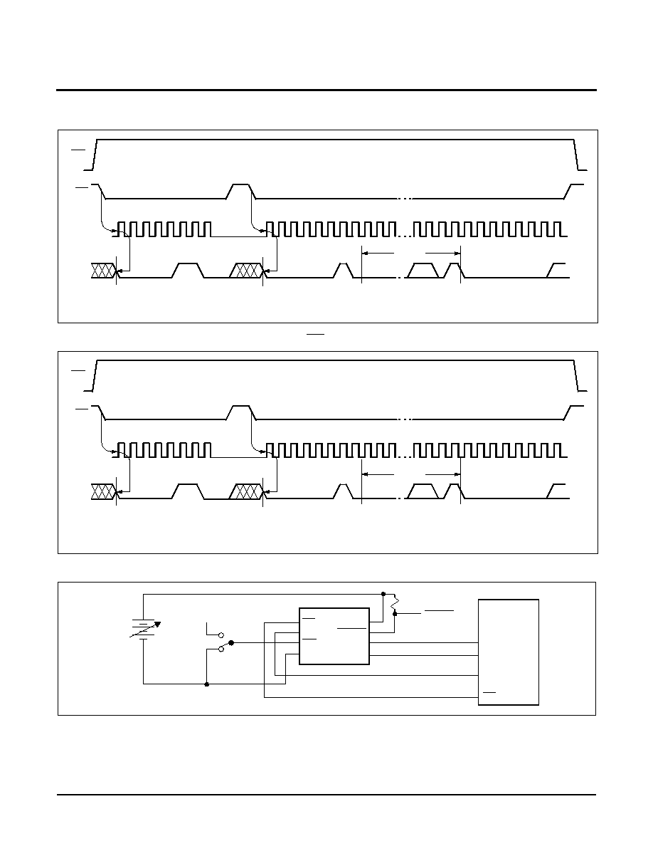
Setting the V
TRIP
Voltage
This procedure is used to set the V
TRIP
to a higher or
lower voltage value. It is necessary to reset the trip
point before setting the new value to a lower level.
To set the new voltage, apply the desired V
TRIP
thresh-
old voltage to the V
CC
pin, then tie the WP pin to the
programming voltage V
P
. Then, send the WREN com-
mand and write to address 01h to program V
TRIP
, (fol-
lowed by data byte 00h). The CS going high after a
valid write operating initiates the programming
sequence. Bring WP LOW to complete the operation.
Note:
This operation will not alter the contents of the
EEPROM.
C
ASE
A
If the V
TRIPX
(actual) is lower than the V
TRIPX
(desired), then add the difference between V
TRIPX
(desired) and V
TRIPX
(actual) to the original V
TRIPX
(desired). This is your new V
TRIPX
voltage that should
be applied to VXMON and the whole sequence
repeated again (see Fig 6).
C
ASE
B
If the V
TRIPX
(actual) is higher than the V
TRIPX
(desired), perform the reset sequence as described in
the next section. The new V
TRIPX
voltage to be applied
to VXMON will now be: V
TRIPX
(desired) ≠ (V
TRIPX
(desired) ≠ V
TRIPX
(actual)).
Resetting the V
TRIP
Voltage
This procedure is used to set the V
TRIP
to a "native"
voltage level. For example, if the current V
TRIP
is 4.4V
and the new V
TRIP
must be 4.0V, then the V
TRIP
must
be reset. When the threshold is reset, the new level is
something less than 1.7V. This procedure must be
used to set the voltage to a lower value.
To reset the new V
TRIP
, apply greater than 3V to V
CC
and tie the WP pin to the programming voltage V
P
.
Then send the WREN command and write to address
0Bh to reset the V
TRIP
(followed by data byte 00h). The
CS going LOW to HIGH after a valid write operation ini-
tiates the programming sequence. Bring WP LOW to
complete the operation.
Note:
This operation does not change the contents of
the EEPROM array.
X5563 ≠ Preliminary Information
Characteristics subject to change without notice.
5 of 18
REV 1.8 9/30/02
www.xicor.com
Figure 1. Set V
TRIP
Level Sequence (V
CC
= desired V
TRIP
)
Figure 2. Reset V
TRIP
Level Sequence (V
CC
> 3V. WP = 10-15V)
Figure 3. Sample V
TRIP
Reset Circuit
0 1 2 3 4 5 6 7
0 1
2 3 4 5 6
CS
SCK
SI
16 Bits
7
8 9 10
20 21 22 23
WP
V
P
= 10-15V
06h
WREN
02h
Write
00h
Data
0001h
Address
Addr 01h: Set V
CC
trip
0 1 2 3 4 5 6 7
0 1
2 3 4 5 6
CS
SCK
SI
16 Bits
7
8 9 10
20 21 22 23
WP
V
P
= 10-15V
06h
WREN
02h
Write
00h
Data
0003h
Address
Addr 03h: Update V
CC
trip
CS
V
CC
V
P
Adjust
Run
V
TRIP
Adj.
SO
WP
V
SS
RESET
SCK
SI
X5563
4.6K
RESET
SO
CS
SI
SCK
µC
X5563 ≠ Preliminary Information
Characteristics subject to change without notice.
6 of 18
REV 1.8 9/30/02
www.xicor.com
Figure 4. V
TRIP
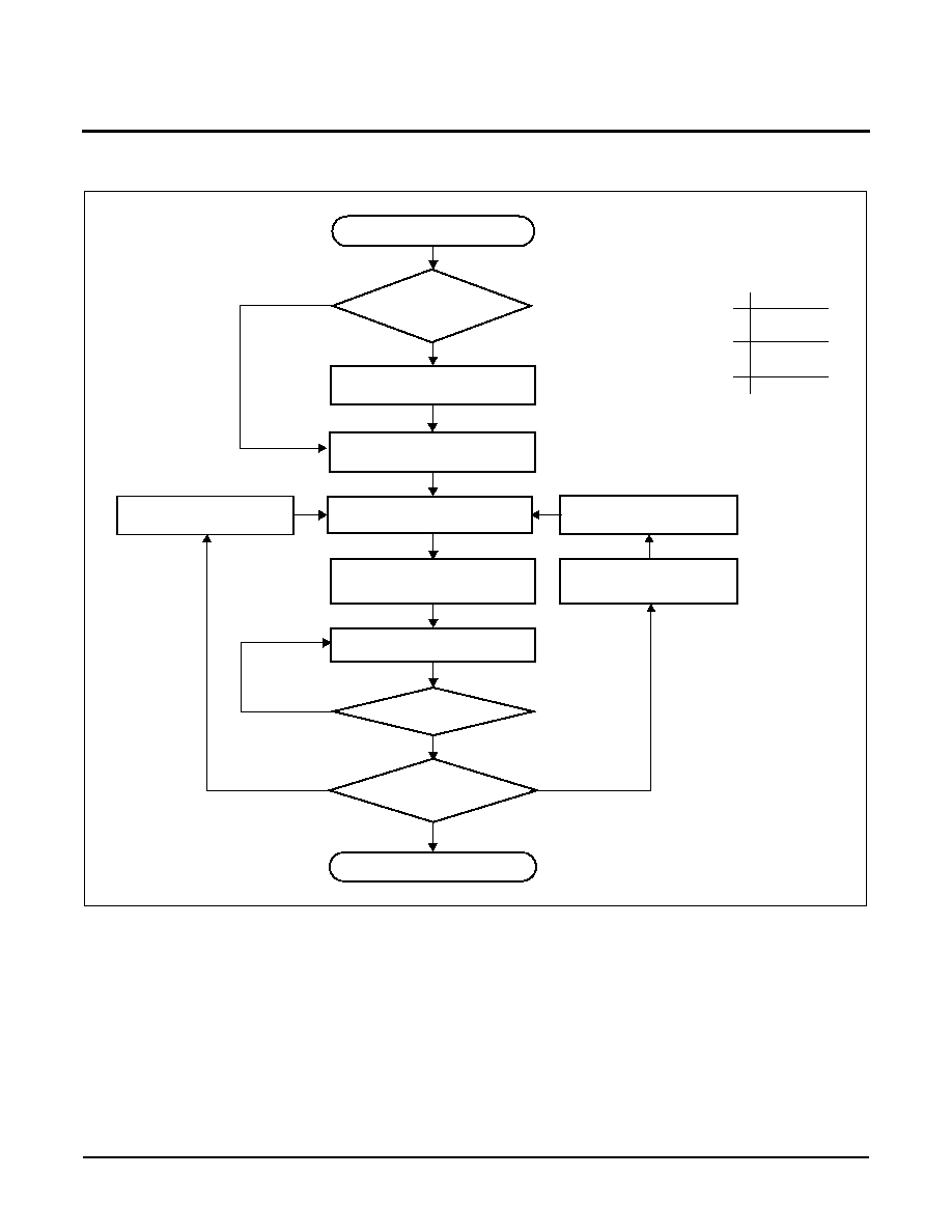
Programming Sequence Flow Chart
V
TRIPX
Programming
Apply V
CC
and Voltage
Decrease V
X
Actual V
TRIPX -
Desired V
TRIPX
DONE
Set Higher V
TRIPX
Sequence
Error < MDE
≠
| Error | < | MDE |
YES
NO
Error > MDE
+
> Desired V
TRIPX
to V
X
Desired
Present Value?
V
TRIPX
<
Execute
No
YES
Execute
V
TRIPX
Reset Sequence
Set
V
X
= desired V
TRIPX
New V
X
applied =
Old V
X
applied + | Error |
New V
X
applied =
Old V
X
applied - | Error |
Execute Reset V
TRIPX
Sequence
Output Switches?
Note: X = 1, 2
Let: MDE = Maximum Desired Error
Vx = VxMON
MDE
+
Desired Value
MDE
≠
Acceptable
Error Range
Error = Actual - Desired
X5563 ≠ Preliminary Information
Characteristics subject to change without notice.
7 of 18
REV 1.8 9/30/02
www.xicor.com
SPI SERIAL MEMORY
The memory portion of the device is a CMOS Serial
EEPROM array with Xicor's block lock protection. The
array is internally organized as x 8. The device features
a Serial Peripheral Interface (SPI) and software protocol
allowing operation on a simple four-wire bus.
The device utilizes Xicor's proprietary Direct Write
TM
cell, providing a minimum endurance of 100,000 cycles
and a minimum data retention of 100 years.
The device is designed to interface directly with the
synchronous Serial Peripheral Interface (SPI) of many
popular microcontroller families. It contains an 8-bit
instruction register that is accessed via the SI input,
with data being clocked in on the rising edge of SCK.
CS must be LOW during the entire operation.
All instructions (Table 1), addresses and data are
transferred MSB first. Data input on the SI line is
latched on the first rising edge of SCK after CS goes
LOW. Data is output on the SO line by the falling edge
of SCK. SCK is static, allowing the user to stop the
clock and then start it again to resume operations
where left off.
Write Enable Latch
The device contains a Write Enable Latch. This latch
must be SET before a Write Operation is initiated. The
WREN instruction will set the latch and the WRDI
instruction will reset the latch (Figure 7). This latch is
automatically reset upon a power-up condition and
after the completion of a valid Write Cycle.
Status Register
The RDSR instruction provides access to the Status
Register. The Status Register may be read at any time,
even during a Write Cycle. The Status Register is for-
matted as follows:
The Write-In-Progress (WIP) bit is a volatile, read only
bit and indicates whether the device is busy with an
internal nonvolatile write operation. The WIP bit is read
using the RDSR instruction. When set to a "1", a non-
volatile write operation is in progress. When set to a
"0", no write is in progress.
7
6
5
4
3
2
1
0
WPEN
WD1
WD0
PUP
BL1
BL0
WEL
WIP
Table 1. Instruction Set
Note:
*Instructions are shown MSB in leftmost position. Instructions are transferred MSB first.
Table 2. Block Protect Matrix
Instruction Name
Instruction Format*
Operation
WREN
0000 0110
Set the Write Enable Latch (Enable Write Operations)
WRDI
0000 0100
Reset the Write Enable Latch
RSDR
0000 0101
Read Status Register
WRSR
0000 0001
Write Status Register (Watchdog, block lock, WPEN)
READ
0000 0011
Read Data from Memory Array Beginning at Selected Address
WRITE
0000 0010
Write Data to Memory Array Beginning at Selected Address
WREN CMD
Status Register
Device Pin
Block
Block
Status Register
WEL
WPEN
WP
Protected Block Unprotected Block
WPEN, BL0, BL1,
PUP, WD0, WD1
0
X
X
Protected
Protected
Protected
1
1
0
Protected
Writable
Protected
1
0
X
Protected
Writable
Writable
1
X
1
Protected
Writable
Writable
X5563 ≠ Preliminary Information
Characteristics subject to change without notice.
8 of 18
REV 1.8 9/30/02
www.xicor.com
The Write Enable Latch (WEL) bit indicates the Status
of the Write Enable Latch. When WEL = 1, the latch is
set HIGH and when WEL = 0 the latch is reset LOW.
The WEL bit is a volatile, read only bit. It can be set by
the WREN instruction and can be reset by the WRDS
instruction.
The block lock bits, BL0 and BL1, set the level of block
lock protection. These nonvolatile bits are programmed
using the WRSR instruction and allow the user to pro-
tect one quarter, one half, all or none of the EEPROM
array. Any portion of the array that is block lock pro-
tected can be read but not written. It will remain pro-
tected until the BL bits are altered to disable block lock
protection of that portion of memory.
The power on reset time (t
PURST
) bit, PUP sets the
initial power or reset time. There are two standard
settings.
The Watchdog Timer bits, WD0 and WD1, select the
Watchdog Time-out Period. These nonvolatile bits are
programmed with the WRSR instruction.
The nonvolatile WPEN bit is programmed using the
WRSR instruction. This bit works in conjunction with
the WP pin to provide an In-Circuit Programmable
ROM function (Table 2). WP is LOW and WPEN bit
programmed HIGH disables all Status Register Write
Operations.
In Circuit Programmable ROM Mode
This mechanism protects the block lock and Watchdog
bits from inadvertent corruption.
In the locked state (Programmable ROM Mode) the
WP pin is LOW and the nonvolatile bit WPEN is "1".
This mode disables nonvolatile writes to the device's
Status Register.
Status Register Bits
Array Addresses Protected
BL1
BL0
X5563
0
0
None
0
1
6000h≠7FFFh
1
0
4000h≠7FFFh
1
1
0000h≠7FFFh
PUP
Time
0
150 milliseconds (factory settings)
1
800 milliseconds
Status Register Bits
Watchdog Time Out
(Typical)
WD1
WD0
0
0
800 milliseconds
0
1
400 milliseconds
1
0
150 milliseconds
1
1
disabled (factory setting)
Figure 5. Read EEPROM Array Sequence
0
1
2
3
4
5
6
7
8
9
10
20 21 22 23 24 25
26 27 28 29 30
7
6
5
4
3
2
1
0
Data Out
CS
SCK
SI
SO
MSB
High Impedance
Instruction
16 Bit Address
15 14 13
3
2
1
0

X5563 ≠ Preliminary Information
Characteristics subject to change without notice.
9 of 18
REV 1.8 9/30/02
www.xicor.com
Setting the WP pin LOW while WPEN is a "1" while an
internal write cycle to the Status Register is in progress
will not stop this write operation, but the operation dis-
ables subsequent write attempts to the Status Register.
When WP is HIGH, all functions, including nonvolatile
writes to the Status Register operate normally. Setting
the WPEN bit in the Status Register to "0" blocks the
WP pin function, allowing writes to the Status Register
when WP is HIGH or LOW. Setting the WPEN bit to "1"
while the WP pin is LOW activates the Programmable
ROM mode, thus requiring a change in the WP pin
prior to subsequent Status Register changes. This
allows manufacturing to install the device in a system
with WP pin grounded and still be able to program the
Status Register. Manufacturing can then load Configu-
ration data, manufacturing time and other parameters
into the EEPROM, then set the portion of memory to
be protected by setting the block lock bits, and finally
set the "OTP mode" by setting the WPEN bit. Data
changes now require a hardware change.
Read Sequence
When reading from the EEPROM memory array, CS is
first pulled low to select the device. The 8-bit READ
instruction is transmitted to the device, followed by the
16-bit address. After the READ opcode and address
are sent, the data stored in the memory at the selected
address is shifted out on the SO line. The data stored
in memory at the next address can be read sequen-
tially by continuing to provide clock pulses. The
address is automatically incremented to the next
higher address after each byte of data is shifted out.
When the highest address is reached, the address
counter rolls over to address $0000 allowing the read
cycle to be continued indefinitely. The read operation is
terminated by taking CS high. Refer to the Read
EEPROM Array Sequence (Figure 5).
To read the Status Register, the CS line is first pulled
low to select the device followed by the 8-bit RDSR
instruction. After the RDSR opcode is sent, the contents
of the Status Register are shifted out on the SO line.
Refer to the Read Status Register Sequence (Figure 6).
Write Sequence
Prior to any attempt to write data into the device, the
"Write Enable" Latch (WEL) must first be set by issuing
the WREN instruction (Figure 7). CS is first taken LOW,
then the WREN instruction is clocked into the device.
After all eight bits of the instruction are transmitted, CS
must then be taken HIGH. If the user continues the
Write Operation without taking CS HIGH after issuing
the WREN instruction, the Write Operation will be
ignored.
To write data to the EEPROM memory array, the user
then issues the WRITE instruction followed by the 16
bit address and then the data to be written. Any
unused address bits are specified to be "0's". The
WRITE operation minimally takes 32 clocks. CS must
go low and remain low for the duration of the operation.
If the address counter reaches the end of a page and
the clock continues, the counter will roll back to the first
address of the page and overwrite any data that may
have been previously written.
For the Page Write Operation (byte or page write) to be
completed, CS can only be brought HIGH after bit 0 of
the last data byte to be written is clocked in. If it is
brought HIGH at any other time, the write operation will
not be completed (Figure 8).
To write to the Status Register, the WRSR instruction is
followed by the data to be written (Figure 9).
While the write is in progress following a Status Register
or EEPROM Sequence, the Status Register may be
read to check the WIP bit. During this time the WIP bit
will be high.
Operational Notes
The device powers-up in the following state:
≠ The device is in the low power standby state.
≠ A HIGH to LOW transition on CS is required to enter
an active state and receive an instruction.
≠ SO pin is high impedance.
≠ The Write Enable Latch is reset.
≠ Reset Signal is active for t
PURST
.
Data Protection
The following circuitry has been included to prevent
inadvertent writes:
≠ A WREN instruction must be issued to set the Write
Enable Latch.
≠ CS must come HIGH at the proper clock count in
order to start a nonvolatile write cycle.
X5563 ≠ Preliminary Information
Characteristics subject to change without notice.
10 of 18
REV 1.8 9/30/02
www.xicor.com
Figure 6. Read Status Register Sequence
Figure 7. Write Enable Latch Sequence
0
1
2
3
4
5
6
7
8
9
10
11 12 13 14
7
6
5
4
3
2
1
0
Data Out
CS
SCK
SI
SO
MSB
High Impedance
Instruction
0
1
2
3
4
5
6
7
CS
SI
SCK
High Impedance
SO

X5563 ≠ Preliminary Information
Characteristics subject to change without notice.
11 of 18
REV 1.8 9/30/02
www.xicor.com
Figure 8. Write Sequence
Figure 9. Status Register Write Sequence
SYMBOL TABLE
32 33 34 35 36 37 38 39
SCK
SI
CS
0
1
2
3
4
5
6
7
8
9
10
SCK
SI
Instruction
16 Bit Address
Data Byte 1
7
6
5
4
3
2
1
0
CS
40 41 42 43 44 45 46 47
Data Byte 2
7
6
5
4
3
2
1
0
Data Byte 3
7
6
5
4
3
2
1
0
Data Byte N
15 14 13
3
2
1
0
20 21 22 23 24 25 26 27 28 29 30 31
6
5
4
3
2
1
0
0
1
2
3
4
5
6
7
8
9
CS
SCK
SI
SO
High Impedance
Instruction
Data Byte
7
6
5
4
3
2
1
0
10
11 12 13 14 15
WAVEFORM
INPUTS
OUTPUTS
Must be
steady
Will be
steady
May change
from LOW
to HIGH
Will change
from LOW
to HIGH
May change
from HIGH
to LOW
Will change
from HIGH
to LOW
Don't Care:
Changes
Allowed
Changing:
State Not
Known
N/A
Center Line
is High
Impedance
X5563 ≠ Preliminary Information
Characteristics subject to change without notice.
12 of 18
REV 1.8 9/30/02
www.xicor.com
ABSOLUTE MAXIMUM RATINGS
Temperature under bias .................. ≠65∞C to +135∞C
Storage temperature ....................... ≠65∞C to +150∞C
Voltage on any pin with
respect to V
SS
......................................≠1.0V to +7V
D.C. output current ............................................... 5mA
Lead temperature (soldering, 10 seconds)........ 300∞C
COMMENT
Stresses above those listed under "Absolute Maximum
Ratings" may cause permanent damage to the device.
This is a stress rating only; functional operation of the
device (at these or any other conditions above those
listed in the operational sections of this specification) is
not implied. Exposure to absolute maximum rating con-
ditions for extended periods may affect device reliability.
RECOMMENDED OPERATING CONDITIONS
Temperature
Min.
Max.
Commercial
0∞C
70∞C
Industrial
≠40∞C
+85∞C
Device Option
Supply Voltage
Blank or -4.5A
4.5V≠5.5V
-2.7 or -2.7A
2.7V≠5.5V
D.C. OPERATING CHARACTERISTICS (Over the recommended operating conditions unless otherwise specified.)
Notes: (1) Address Byte are incorrect; 200ns after a stop ending a read operation; or t
WC
after a stop ending a write operation.
(2) The device goes into Standby: 200ns after any Stop, except those that initiate a high voltage write cycle; t
WC
after a stop that initiates a
high voltage cycle; or 9 clock cycles after any start that is not followed by the correct Device Select Bits in the Slave Address Byte.
(3) Negative number indicate charging current, Positive numbers indicate discharge current.
(4) V
IL
min. and V
IH
max. are for reference only and are not tested.
Symbol
Parameter
Limits
Unit
Test Conditions
Min.
Typ.
Max.
I
CC1
(1)
V
CC
Supply Current (Active)
Read Memory array
Write nonvolatile Memory
1.5
3.0
mA
SCK = V
CC
x 0.1/
V
CC
x 0.9 @ 10MHz
I
CC2
(2)
V
CC
Supply Current (Passive)
WDT on, V
CC
= 5V
WDT on, V
CC
= 2.7V
WDT off, V
CC
= 5V
50.0
40.0
30.0
90.0
60.0
50.0
µA
CS = V
CC
, Any
Input= V
SS
or V
CC
RESET, SO = Open
RESET
V
TRIP
V
CC
Reset Trip Point Voltage
4.5
4.62
4.75
V
-4.5A version
4.25
4.38
4.50
V
-4.5 version
2.85
2.93
3.0
V
-2.7A version
2.55
2.63
2.7
V
-2.7 version
V
OLR
Output (RESET) LOW Voltage
0.4
V
I
OL
= 3.0mA (5V)
I
OL
= 1.0mA (3V)
SPI Interface
V
ILx
(4)
Input (CS, SI, SCK, WP) LOW Voltage
-0.5
V
CC
x 0.3
V
V
IHx
(4)
Input (CS, SI, SCK, WP) HIGH Voltage
V
CC
x 0.7
V
CC
+ 0.5
V
I
LIx
Input Leakage Current (CS, SI, SCK, WP)
±10
µA
V
OLS
Output (SO) LOW Voltage
0.4
V
I
OL
= 3.0mA (5V)
I
OL
= 1.0mA (3V)
V
OHS
Output (SO) HIGH Voltage
V
CC
≠ 0.8
V
I
OH
= -1.0mA (5V)
X5563 ≠ Preliminary Information
Characteristics subject to change without notice.
13 of 18
REV 1.8 9/30/02
www.xicor.com
CAPACITANCE T
A
= +25∞C, f = 1MHz, V
CC
= 5V
Note:
(1) This parameter is periodically sampled and not 100% tested.
Symbol
Test
Max.
Unit
Conditions
C
OUT
(1)
Output Capacitance (SO, RESET)
8
pF
V
OUT
= 0V
C
IN
(1)
Input Capacitance (SCK, SI, CS, WP)
6
pF
V
IN
= 0V
EQUIVALENT A.C. LOAD CIRCUIT AT 5V V
CC
A.C. TEST CONDITIONS
5V
SO
30pF
RESET
2.06K
3.03K
V
CC
1.53K
30pF
Input pulse levels
V
CC
x 0.1 to V
CC
x 0.9
Input rise and fall times
10ns
Input and output timing level
V
CC
x0.5
A.C. CHARACTERISTICS (Over recommended operating conditions, unless otherwise specified)
Serial Input Timing
Symbol
Parameter
2.7≠5.5V
Unit
Min.
Max.
f
SCK
Clock Frequency
0
10
MHz
t
CYC
Cycle Time
100
ns
t
LEAD
CS Lead Time
50
ns
t
LAG
CS Lag Time
200
ns
t
WH
Clock HIGH Time
40
ns
t
WL
Clock LOW Time
40
ns
t
SU
Data Setup Time
10
ns
t
H
Data Hold Time
10
ns
t
RI
(3)
Input Rise Time
20
ns
t
FI
(3)
Input Fall Time
20
ns
t
CS
CS Deselect Time
50
ns
t
WC
(4)
Write Cycle Time
10
ms
X5563 ≠ Preliminary Information
Characteristics subject to change without notice.
14 of 18
REV 1.8 9/30/02
www.xicor.com
Serial Input Timing
Serial Output Timing
Notes: (3) This parameter is periodically sampled and not 100% tested.
(4) t
WC
is the time from the rising edge of CS after a valid write sequence has been sent to the end of the self-timed internal nonvolatile
write cycle.
Serial Output Timing
Symbol
Parameter
2.7≠5.5V
Unit
Min.
Max.
f
SCK
Clock Frequency
0
10
MHz
t
DIS
Output Disable Time
50
ns
t
V
Output Valid from Clock Low
40
ns
t
HO
Output Hold Time
0
ns
t
RO
(3)
Output Rise Time
25
ns
t
FO
(3)
Output Fall Time
25
ns
SCK
CS
SI
SO
MSB IN
t
SU
t
RI
t
LAG
t
LEAD
t
H
LSB IN
t
CS
t
FI
High Impedance
SCK
CS
SO
SI
MSB Out
MSB≠1 Out
LSB Out
ADDR
LSB IN
t
CYC
t
V
t
HO
t
WL
t
WH
t
DIS
t
LAG
X5563 ≠ Preliminary Information
Characteristics subject to change without notice.
15 of 18
REV 1.8 9/30/02
www.xicor.com
Power-Up and Power-Down Timing
RESET Output Timing
CS/WDI vs. RESET Timing
RESET Output Timing
Notes: (1) V
CC
= 5V at 25∞C.
(2) Based on characterization data only.
Symbol
Parameter
Min.
Typ.
(1)
Max.
Unit
t
PURST
RESET Time Out Period
PUP = 0
PUP = 1
75
500
150
800
250
1200
ms
ms
t
RPD
(1)
V
TRIP
to RESET (Power down only)
10
20
µs
t
F
(2)
V
CC
Fall Time
1000
µs
t
R
(2)
V
CC
Rise Time
1000
µs
V
RVALID
Reset Valid V
CC
1
V
Symbol
Parameter
Min.
Typ.
(1)
Max.
Unit
t
WDO
Watchdog Time Out Period,
WD1 = 1, WD0 = 0
WD1 = 0, WD0 = 1
WD1 = 0, WD0 = 0
75
200
500
150
400
(2)
800
(2)
250
600
1200
ms
ms
ms
t
CST
CS Pulse Width to Reset the Watchdog
400
ns
t
RST
Reset Time Out
75
150
250
ms
RESET
t
PURST
t
PURST
t
RPD
V
BATT
V
TRIP
0V
V
CC
t
F
t
R
CS/WDI
t
CST
RESET
t
WDO
t
RST
t
WDO
t
RST
X5563 ≠ Preliminary Information
Characteristics subject to change without notice.
16 of 18
REV 1.8 9/30/02
www.xicor.com
V
TRIP
Set/Reset Conditions
V
TRIP
Programming Specifications V
CC
= 2.5≠5.5V; Temperature = 0∞C to 70∞C
Parameter
Description
Min.
Max.
Unit
t
VPS
WP V
TRIP
Program Voltage Setup time
10
µs
t
VPH
WP V
TRIP
Program Voltage Hold time
10
µs
t
TSU
V
TRIP
Level Setup time
10
µs
t
THD
V
TRIP
Level Hold (stable) time
10
ms
t
WC
V
TRIP
Write Cycle Time
10
ms
t
VPO
WP V
TRIP
Program Voltage Off time before next cycle
1
ms
V
P
Programming Voltage
10
15
V
V
TRAN
V
TRIP
Programed Voltage Range
2.5
5.0
V
V
tv
V
TRIP
Program variation after programming (0≠75∞C). (Programmed at 25∞C
according to the procedure defined in the "principles of operation" section)
-25
+25
mV
V
TRIP
programming parameters are periodically sampled and are not 100% tested.
SCK
CS
* 0001h Set 0h
02h
V
CC
WP
t
THD
t
VPH
t
VPS
V
P
V
TRIPX
t
WC
t
VPO
t
PCS
06h
* 000Bh (Reset)
SI
t
TSU
* all others reserved
8
clocks
(V
TRIP
)
X5563 ≠ Preliminary Information
Characteristics subject to change without notice.
17 of 18
REV 1.8 9/30/02
www.xicor.com
PACKAGING INFORMATION
0.150 (3.80)
0.158 (4.00)
0.228 (5.80)
0.244 (6.20)
0.014 (0.35)
0.019 (0.49)
Pin 1
Pin 1 Index
0.010 (0.25)
0.020 (0.50)
0.050 (1.27)
0.188 (4.78)
0.197 (5.00)
0.004 (0.19)
0.010 (0.25)
0.053 (1.35)
0.069 (1.75)
(4X) 7∞
0.016 (0.410)
0.037 (0.937)
0.0075 (0.19)
0.010 (0.25)
0∞ - 8∞
X 45∞
8-Lead Plastic Small Outline Gull Wing Package Type S
NOTE: ALL DIMENSIONS IN INCHES (IN PARENTHESES IN MILLIMETERS)
0.250"
0.050"Typical
0.050"
Typical
0.030"
Typical
8 Places
FOOTPRINT
X5563 ≠ Preliminary Information
Characteristics subject to change without notice.
18 of 18
LIMITED WARRANTY
Devices sold by Xicor, Inc. are covered by the warranty and patent indemnification provisions appearing in its Terms of Sale only. Xicor, Inc. makes no warranty,
express, statutory, implied, or by description regarding the information set forth herein or regarding the freedom of the described devices from patent infringement.
Xicor, Inc. makes no warranty of merchantability or fitness for any purpose. Xicor, Inc. reserves the right to discontinue production and change specifications and prices
at any time and without notice.
Xicor, Inc. assumes no responsibility for the use of any circuitry other than circuitry embodied in a Xicor, Inc. product. No other circuits, patents, or licenses are implied.
TRADEMARK DISCLAIMER:
Xicor and the Xicor logo are registered trademarks of Xicor, Inc. AutoStore, Direct Write, Block Lock, SerialFlash, MPS, and XDCP are also trademarks of Xicor, Inc. All
others belong to their respective owners.
U.S. PATENTS
Xicor products are covered by one or more of the following U.S. Patents: 4,326,134; 4,393,481; 4,404,475; 4,450,402; 4,486,769; 4,488,060; 4,520,461; 4,533,846;
4,599,706; 4,617,652; 4,668,932; 4,752,912; 4,829,482; 4,874,967; 4,883,976; 4,980,859; 5,012,132; 5,003,197; 5,023,694; 5,084,667; 5,153,880; 5,153,691;
5,161,137; 5,219,774; 5,270,927; 5,324,676; 5,434,396; 5,544,103; 5,587,573; 5,835,409; 5,977,585. Foreign patents and additional patents pending.
LIFE RELATED POLICY
In situations where semiconductor component failure may endanger life, system designers using this product should design the system with appropriate error detection
and correction, redundancy and back-up features to prevent such an occurrence.
Xicor's products are not authorized for use in critical components in life support devices or systems.
1. Life support devices or systems are devices or systems which, (a) are intended for surgical implant into the body, or (b) support or sustain life, and whose failure to
perform, when properly used in accordance with instructions for use provided in the labeling, can be reasonably expected to result in a significant injury to the user.
2. A critical component is any component of a life support device or system whose failure to perform can be reasonably expected to cause the failure of the life
support device or system, or to affect its safety or effectiveness.
©Xicor, Inc. 2001 Patents Pending
REV 1.8 9/30/02
www.xicor.com
Part Mark Information
S8= 8 Lead SOIC
W
X5563
X
YYww
Date
Code
Part
Mark
V
TRIP
Range
Operating Temperature Range
Part Number RESET
AL
4.5≠4.75
0∞C≠70∞C
X5563S8-4.5A
AM
-40∞C≠85∞C
X5563S8I-4.5A
Blank
4.25≠4.5
0∞C≠70∞C
X5563S8
I
-40∞C≠85∞C
X5563S8I
AN
2.85≠3.0
0∞C≠70∞C
X5563S8-2.7A
AP
-40∞C≠85∞C
X5563S8I-2.7A
F
2.55≠2.7
0∞C≠70∞C
X5563S8-2.7
G
-40∞C≠85∞C
X5563S8I-2.7