 | –≠–ª–µ–∫—Ç—Ä–æ–Ω–Ω—ã–π –∫–æ–º–ø–æ–Ω–µ–Ω—Ç: X76F041W | –°–∫–∞—á–∞—Ç—å:  PDF PDF  ZIP ZIP |
Document Outline
- Table of Contents
- Product Selection
- Data Sheet Alpha
- Ap Note Alpha
Password Access Security Supervisor
©Xicor, Inc. 1994, 1995, 1996 Patents Pending
7002-2.2 4/30/97 T3/C0/D0 SH
1
Characteristics subject to change without notice
4K
X76F041
4 x 128 x 8 Bit
PASS
TM
SecureFlash
FEATURES
∑ 64-Bit Password Security
∑ Three Password Modes
--Secure Read Access
--Secure Write Access
--Secure Configuration Access
∑ Programmable Configuration
--Read, Write and Configuration Access
Passwords
--Multiple Array Access/Functionality
--Retry Register/Counter
∑ 8 Byte Sector Write
∑ (4) 1K Memory Arrays
∑ ISO Response to Reset
∑ Low Power CMOS
--50
µ
A Standby Current
--3mA Active Current
∑ 1.8V to 3.6V or 5V "Univolt" Read and Program
Power Supply Versions
∑ High Reliability
--Endurance: 100,000 Cycles
--Data Retention: 100 Years
--ESD Protection: 2000V on All Pins
DESCRIPTION
The X76F041 is a password access security supervisor
device, containing four 128 x 8 bit SecureFlash arrays.
Access can be controlled by three 64-bit programmable
passwords, one for read operations, one for write opera-
tions and one for device configuration.
The X76F041 features a serial interface and software
protocol allowing operation on a simple two wire bus. The
bus signals are a clock input (SCL) and a bidirectional
data input and output (SDA). Access to the device is con-
trolled through a chip select input (CS), allowing any
number of devices to share the same bus.
The X76F041 also features a synchronous response to
reset; providing an automatic output of a pre-configured
32-bit data stream conforming to the ISO standard for
memory cards.
The X76F041 utilizes Xicor's proprietary Direct Write
TM
cell, providing a minimum endurance of 100,000 cycles
per sector and a minimum data retention of 100 years.
FUNCTIONAL DIAGRAM
INTERFACE
LOGIC
CHIP
ENABLE
(4) 16 x 64
SECUREFLASH
ARRAYS
180≠1FF
100≠17F
080≠0FF
000≠07F
SDA
SCL
RST
CS
7002 ILL F01
DATA
TRANSFER
ARRAY ACCESS
ENABLE
PASSWORD ARRAY AND
PASSWORD VERIFICATION
LOGIC
ISO RESET RESPONSE
DATA REGISTER
CONFIGURATION
REGISTER
RETRY
COUNTER
A
PPLICATION
N
OTE
A V A I L A B L E
AN83 ∑ Development Tools XK76C

X76F041
2
PIN DESCRIPTION
Serial Data Input/Output (SDA)
SDA is a true three state serial data input/output pin.
During a read cycle, data is shifted out on this pin.
During a write cycle, data is shifted in on this pin. In all
other cases this pin is in a high impedance state.
Serial Clock (SCL)
The Serial Clock controls the serial bus timing for data
input and output.
Chip Select (CS)
When CS is HIGH, the X76F041 is deselected and the
SDA pin is at high impedance and unless an internal
write operation is underway the X76F041 will be in the
standby power mode. CS LOW enables the X76F041,
placing it in the active power mode.
Reset (RST)
RST is a device reset pin. When RST is pulsed HIGH
while CS is LOW the X76F041 will output 32 bits of
fixed data which conforms to the ISO standard for
"synchronous response to reset". CS must remain
LOW and the part must not be in a write cycle for the
response to reset to occur. If at any time during the
response to reset CS goes HIGH, the response to
reset will be aborted and the part will return to the
standby mode.
PIN CONFIGURATION
7002 FRM T01
Symbol
Description
CS
Chip Select Input
SDA
Serial Data Input/Output
RST
Reset Input
SCL
Serial Clock Input
V
SS
Ground
V
CC
Supply Voltage
NC
No Connect
7002 ILL F02
VCC
RST
SCL
NC
1
2
3
4
8
7
6
5
VSS
CS
SDA
NC
X76F041
DIP/SOIC
X76F041
3
DEVICE OPERATION
There are three primary modes of operation for the
X76F041; READ, WRITE and CONFIGURATION. The
READ and WRITE modes may be performed with or
without an 8-byte password. The CONFIGURATION
mode always requires an 8-byte password.
The basic method of communication is established by
first enabling the device (CS LOW), generating a start
condition and then transmitting a command and address
field followed by the correct password (if configured to
require a password). All parts will be shipped from the
factory in the non-password mode. The user must per-
form an ACK Polling routine to determine the validity of
the password and start the data transfer (see Acknowl-
edge Polling). Only after the correct password is
accepted and an ACK Polling has been performed can
the data transfer occur.
To ensure correct communication, RST must remain
LOW under all conditions except when initiating a
"Response to Reset sequence".
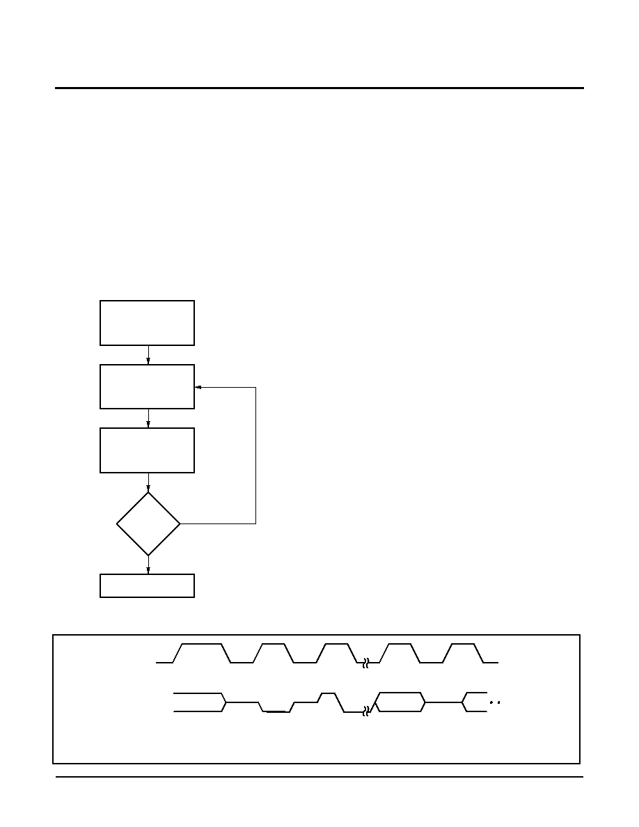
Figure 1. X76F041 Device Operation
Data is transferred in 8-bit segments, with each transfer
being followed by an ACK, generated by the receiving
device.
If the X76F041 is in a nonvolatile write cycle a "no ACK"
(SDA HIGH) response will be issued in response to load-
ing of the command + high order address byte. If a stop
condition is issued prior to the nonvolatile write cycle the
write operation will be terminated and the part will reset
and enter into a standby mode.
The basic sequence is illustrated in Figure 1.
After each transaction is completed, the X76F041 will
reset and enter into a standby mode. This will also be the
response if an attempt is made to access any limited
array.
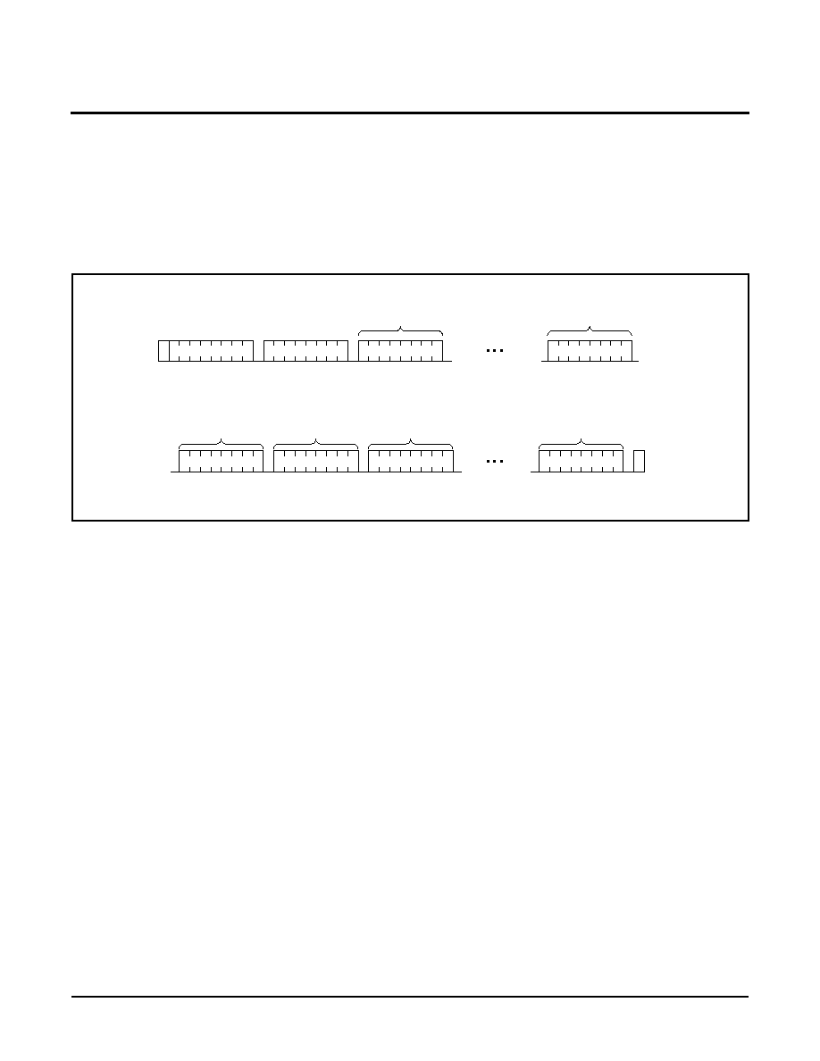
Password Registers
The three passwords, Read, Write and Configuration
are stored in three 64 bit Write Only registers as illus-
trated in figure 2.
Figure 2. Password Registers
Device Configuration
Five 8-Bit configuration registers are used to configure
the X76F041. These are shown in figure 3.
Figure 3. Configuration Registers
LOAD
LOW ORDER ADDRESS / CONFIGURATION INSTRUCTION
BYTE
LOAD 8≠BYTE PASSWORD
(IF APPLICABLE)
VERIFY PASSWORD ACCEPTANCE BY USE
OF ACK POLLING (IF APPLICABLE)
READ / WRITE
DATA BYTES
LOAD
COMMAND+HIGH ORDER ADDRESS
BYTE
7002 ILL F03
64 BIT WRITE PASSWORD
64 BIT READ PASSWORD
64 BIT CONFIGURATION PASSWORD
63
0
7002 ILL F04
ACR1
ACR2
CR
RR
RC
RES
RES
RES
RESERVED
RETRY REGISTER
CONFIGURATION REGISTER
ARRAY CONTROL REGISTER 2
ARRAY CONTROL REGISTER 1
RETRY COUNTER
7002 ILL F04B
63
0
X76F041
4
Array Control
The four 1K arrays, are each programmable to different
levels of access and functionality. Each array can be pro-
grammed to require or not require the read/write pass-
words. The functional options are:
∑ Read and Write Access.
∑ Read access with all write operations locked out.
∑ Read access and program only (writing a "1" to a
"0"). If an attempt to change a "0" to a "1" occurs the
X76F041 will reset, issue a "no ACK" and enter the
standby power mode.
∑ No read or write access to the memory. Access only
through use of the configuration password.
Array Map
8 Bit Array Control Register 1
8 Bit Array Control Register 2
Functional Bits
7002 FRM T02
Z
T
FUNCTIONALITY
0
0
READ AND WRITE UNLIMITED
1
0
READ ONLY, WRITE LIMITED
0
1
PROGRAM & READ ONLY,
ERASE LIMITED
1
1
NO READ OR WRITE, FULLY
LIMITED
Addresses 000 07F (hex)
Addresses 080 0FF (hex)
Addresses 100 17F (hex)
Addresses 180 1FF (hex)
First `1k'
Second `1k'
Third `1k'
Fourth `1k'
High-order
Addresses
7002 ILL F04A
X2
Y2
Z2
T2
X1
Y1
Z1
T1
SECOND 1K
FIRST 1K
ACCESS
FUNCTION
ACCESS
FUNCTION
MSB
LSB
7002 ILL F05A
X4
Y4
Z4
T4
X3
Y3
Z3
T3
UPPER 1K
THIRD 1K
ACCESS
FUNCTION
ACCESS
FUNCTION
MSB
LSB
7002 ILL F05B
Access Bits
7002 FRM T03
8-Bit Configuration Register
Unauthorized Access Bits (UA1, UA2):
1 0
Access is forbidden if retry register equals the retry
counter (provided that the retry counter is enabled) and
no further access of any kind will be allowed.
0 1, 0 0, 1 1
Only configuration operations are allowed if the retry reg-
ister equals the retry counter (provided that the retry
counter is enabled).
Retry Counter Reset Bit (RCR):
If the retry counter reset bit is a "1" then the retry counter
will be reset following a correct password, provided the
retry counter is enabled.
If the retry counter reset bit is a "0" then the retry counter
will not be reset following a correct password, provided
the retry counter is enabled.
Retry Counter Enable Bit (RCE):
If the Retry counter enable bit is a "1", then the retry
counter is enabled. An initial comparison between the
retry register and retry counter determines whether the
number of allowed incorrect password attempts has
been reached. If not, the protocol continues and in case
of a wrong password, the retry counter is incremented by
one. If the password is correct then the retry counter will
either be reset or unchanged, depending on the reset bit.
X
Y
READ
PASSWORD
WRITE
PASSWORD
0
0
NOT REQUIRED
NOT REQUIRED
1
0
NOT REQUIRED
REQUIRED
0
1
REQUIRED
NOT REQUIRED
1
1
REQUIRED
REQUIRED
UA1
UA2
1
0
RCR
RCE
0
0
RESERVED
RETRY COUNTER RESET
RESERVED
RESERVED
UNAUTHORIZED ACCESS BIT 2
RETRY COUNTER ENABLE
UNAUTHORIZED ACCESS BIT 1
MSB
LSB
7002 ILL F06
X76F041
5
The retry register must have a higher value than the retry
counter for correct device operation. If the retry counter
value is larger than the retry register and the retry
counter is enabled, the device will wrap around allowing
up to an additional 255 incorrect access attempts.
If the Retry counter enable bit is a "0", then the retry
counter is disabled.
Retry Register/Counter
Both the retry register and retry counter are accessible in
the configuration mode and may be programmed with a
value of 0 to 255.
The difference between the retry register and the retry
counter is the number of access attempts allowed, there-
fore the retry counter must be programmed to a smaller
value than the retry register to prevent wrap around.
DEVICE PROTOCOL
The X76F041 supports a bidirectional bus oriented pro-
tocol. The protocol defines any device that sends data
onto the bus as a transmitter, and the receiving device as
the receiver. The device controlling the transfer is a mas-
ter and the device being controlled is the slave. The mas-
ter will always initiate data transfers, and provide the
clock for both transmit and receive operations. Therefore,
the X76F041 will be considered a slave in all applica-
tions.
Start Condition
All commands except for response to reset are preceded
by the start condition, which is a HIGH to LOW transition
of SDA when SCL is HIGH. The X76F041 continuously
monitors the SDA and SCL lines for the start condition
and will not respond to any command until this condition
has been met.
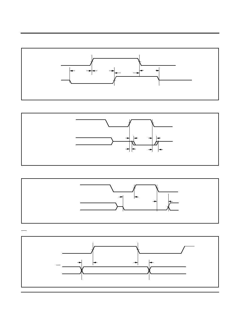
Figure 4. Data Validity During Write
Figure 5. Definition of Start and Stop
NOTE:
The part requires the SCL input to be LOW during non-active periods of operation. In other words, the SCL will need to be LOW prior to
any START condition and LOW after a STOP condition. This is also reflected in the timing diagram.
SCL
SDA
DATA STABLE
DATA
CHANGE
7002 ILL F07
SCL
SDA
START BIT
STOP BIT
7002 ILL F08

X76F041
6
Stop Condition
All communications must be terminated by a stop condi-
tion, which is a LOW to HIGH transition of SDA when
SCL is HIGH. A stop condition can only be issued after
the transmitting device has released the bus.
Acknowledge
Acknowledge is a software convention used to indicate
successful data transfer. The transmitting device, either
master or slave, will release the bus after transmitting
eight bits. During the ninth clock cycle the receiver will
pull the SDA line LOW to acknowledge that it received
the eight bits of data.
OPERATIONAL MODES
7002 FRM T04
THE FIRST BYTE
IN THE PROTOCOL
THE SECOND BYTE
IN THE PROTOCOL
COMMAND DESCRIPTION
PASSWORD USED:
0 0 0XXXXA
Write address
Write (Sector)
Write
0 0 1XXXXA
Read address
Read (Random / Sequential)
Read
0 1 0XXXXA
Write address
Write (Sector)
Configuration
0 1 1XXXXA
Read address
Read (Random / Sequential)
Configuration
1 0 0XXXXX
0 0 0 0 0 0 0 0
Program write-password
Write
1 0 0XXXXX
0 0 0 1 0 0 0 0
Program read-password
Read
1 0 0XXXXX
0 0 1 0 0 0 0 0
Program configuration-password
Configuration
1 0 0XXXXX
0 0 1 1 0 0 0 0
Reset write password (all 0's)
Configuration
1 0 0XXXXX
0 1 0 0 0 0 0 0
Reset read password (all 0's)
Configuration
1 0 0XXXXX
0 1 0 1 0 0 0 0
Program configuration registers
Configuration
1 0 0XXXXX
0 1 1 0 0 0 0 0
Read configuration registers
Configuration
1 0 0XXXXX
0 1 1 1 0 0 0 0
Mass program
Configuration
1 0 0XXXXX
1 0 0 0 0 0 0 0
Mass erase
Configuration
All the rest
Reserved
X76F041
7
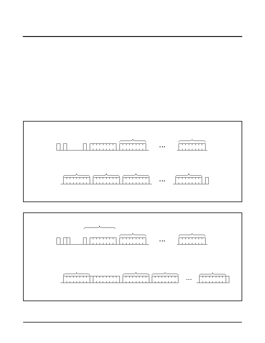
WRITE OPERATION
Sector Write
The Sector Write mode requires issuing the 3-bit write
command followed by the address, password if required
and then the data bytes transferred as illustrated in Fig-
ure 6. Eight bytes must be transferred. After the last byte
to be transferred is acknowledged, a stop condition is
issued, which starts the nonvolatile write cycle. If more
than 8 bytes are transferred the data will wrap around
and previous data will be overwritten. All data will be writ-
ten to the same sector as defined by A
8
≠A
3
.
Figure 6. Sector Write
S
T
A
R
T
S
C M D A
X
A
X
A
X
A
X
A
8
A
7
A
6
A
5
A
4
A
3
A
2
A
1
A
0
A
C
K
WRITE
PASSWORD 7
A
C
K
A
C
K
A
C
K
A
C
K
WRITE
PASSWORD 0
WAIT
tWC/ACK POLLING
DATA 0
A
C
K
A
C
K
S
T
O
P
SDA LINE
IF PASSWORD
MATCH THEN
S
DATA 7
WAIT
tWC
DATA 1
DATA 2
A
C
K
A
C
K
A
C
K
7002 ILL F10.1
X76F041
8
ACK Polling
Once a stop condition is issued to indicate the end of the
host's write sequence, the X76F041 initiates the internal
nonvolatile write cycle. In order to take advantage of the
typical 5ms write cycle, ACK polling can be initiated
immediately. This involves issuing the Start condition fol-
lowed by the new command code of eight bits (1st byte of
the protocol). If the X76F041 is still busy with the nonvol-
atile write operation, it will issue a "no ACK" in response.
If the nonvolatile write operation has completed, an
"ACK" will be returned and the host can then proceed
with the rest of the protocol. Refer to the following flow:
ACK Polling Sequence
7002 ILL F12A
WRITE SEQUENCE
COMPLETED
ENTER ACK POLLING
ISSUE
A START
ISSUE NEW
COMMAND CODE
(1ST BYTE)
ACK
RETURNED
PROCEED
NO ACK (SDA HIGH)
YES (SDA LOW)
After a password sequence, there is always a nonvolatile
write cycle. In order to continue the transaction, the
X76F041 requires the master to perform an ACK polling
with the specific code of C0h. As with regular acknowl-
edge polling the user can either time out for 10ms, and
then issue the ACK polling once, or continuously loop as
described in the flow.
As with regular acknowledge polling, if the user chooses
to loop, then as long as the nonvolatile write cycle is
active, a no ACK will be issued in response to each poll-
ing cycle.
If the password that was inserted was correct, then an
"ACK" will be returned once the nonvolatile write cycle is
over, in response to the ACK polling cycle immediately
following it.
If the password that was inserted was incorrect, then a
"no ACK" will be returned even if the nonvolatile write
cycle is over. Therefore, the user cannot be certain that
the password is incorrect until the 10ms write cycle time
has elapsed.
Figure 7. Acknowledge Polling
SCL
SDA
8th clk.
of 8th
pwd. byte
`ACK'
clk
8th
clk
ACK
clk
8th
bit
`ACK'
ACK or
no ACK
START
condition
7002 ILL F11
X76F041
9
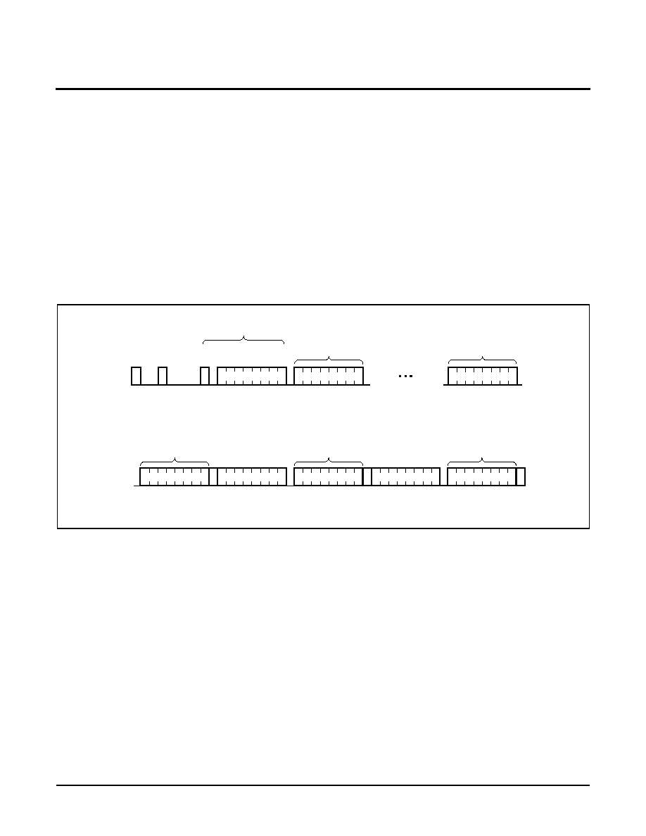
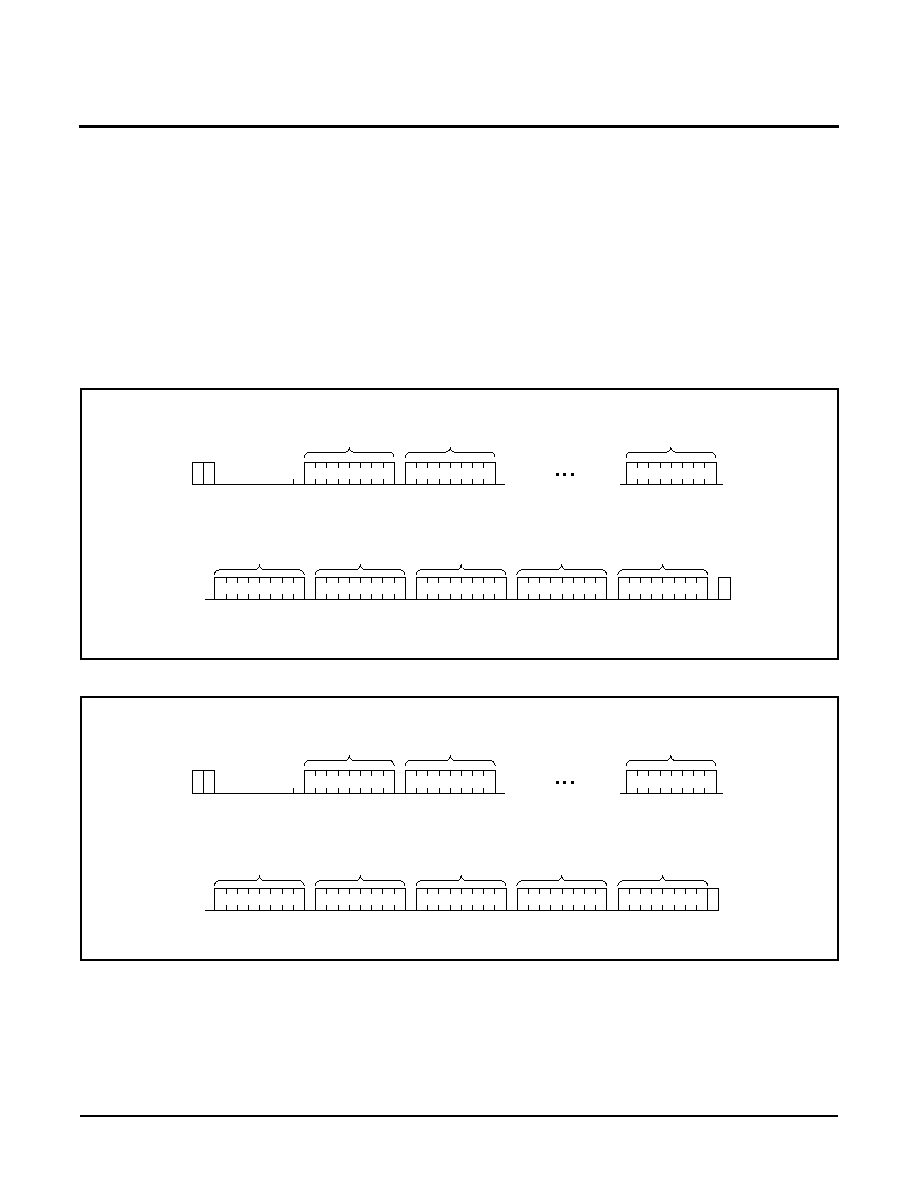
READ OPERATION
Random Read with Password
Random read with password operations are initiated
with a START command followed by the read command
and the address of the first byte of the block in which data
is to be read:
Block 0 = 000h
Block 1 = 080h
Block 2 = 100h
Block 3 = 180h
This is followed by the eight byte read password
sequence which includes the 10ms wait time and the
password acknowledge polling sequence. If the pass-
word is accepted an "ACK" will be returned followed by
eight bits of "secure read setup" which is to be ignored. At
this point a START is issued followed by the address and
data to be read within the original 1K block. See figure 8.
Once the first byte has been read, another start can be
issued followed by a new 8-bit address. Random reads
are allowed only within the original 1K-bit block. To
access another 1K-bit block, a stop must be issued fol-
lowed by a new command/block address/password
sequence.
Figure 8. Random Read with Password
S
T
A
R
T
S
C M D A
X
A
X
A
X
A
X
A
8
A
7
A
6
A
5
A
4
A
3
A
2
A
1
A
0
A
C
K
READ
PASSWORD 7
A
C
K
A
C
K
A
C
K
A
C
K
READ
PASSWORD 0
SECURE
READ SETUP
A
C
K
S
T
A
R
T
SDA LINE
IF PASSWORD
MATCH THEN
DATA 0
A
C
K
S
T
A
R
T
S
S
7002 ILL F13
A
7
A
6
A
5
A
4
A
3
A
2
A
1
A
0
WAIT
tWC/ACK POLLIN
A
7
A
6
A
5
A
4
A
3
A
2
A
1
A
0
DATA 1
A
C
K
S
T
O
P
S
FIRST BYTE
BLOCK ADDRESS
X X X X X X X X
X76F041
10
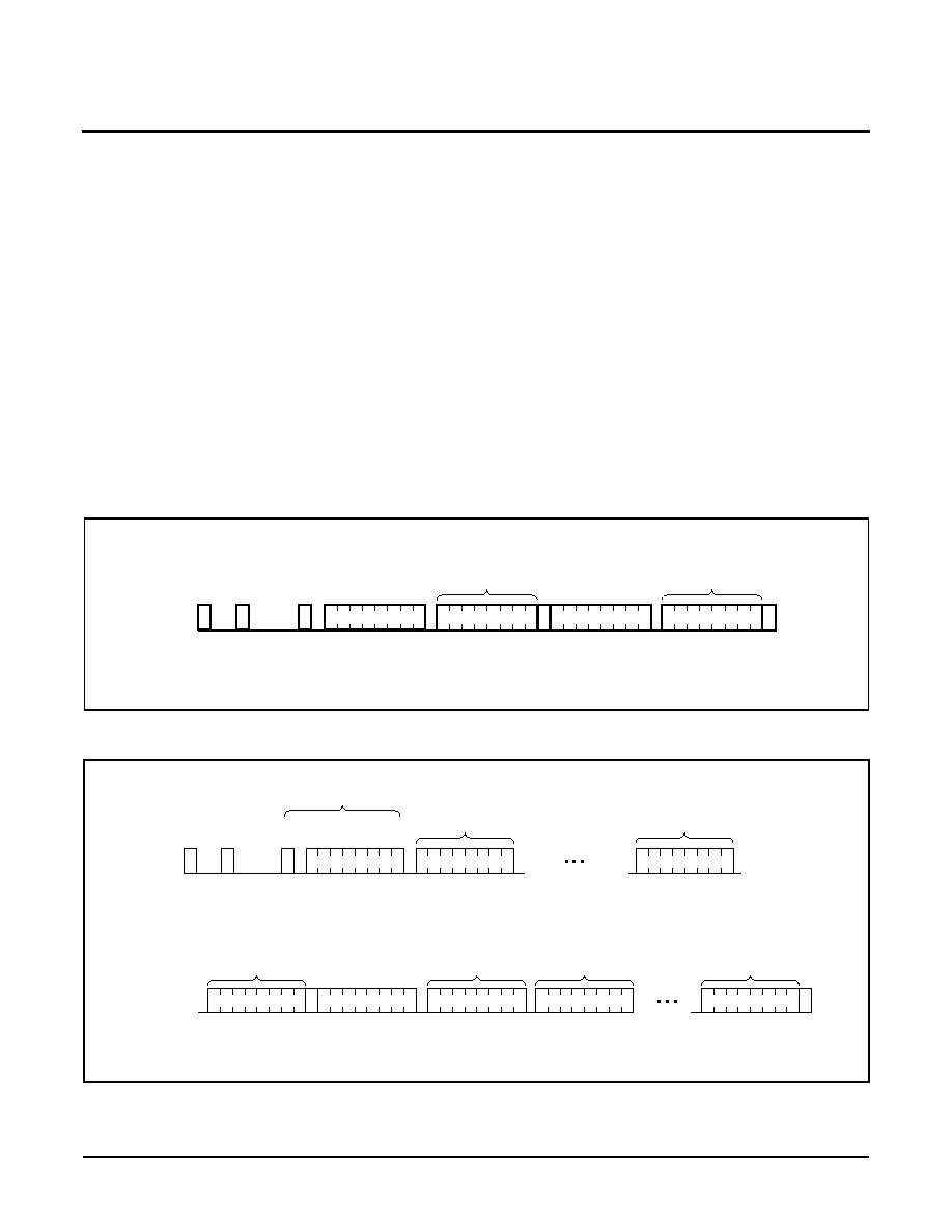
Random Read without Password
Random read operations without a password do not
require the first byte block initiation address. To perform a
random read without password, a START is followed by
the read command plus address location of the byte to
be read. This is followed by an "ACK" and the eight bits of
data to be read. Other bytes within the same 1K-bit block
may be read by issuing another START followed by a
new 8-bit address as shown in figure 9.
Sequential Read
Once past the password acceptance sequence (when
required) and "secure read setup", the host can read
sequentially within the originally addressed 1K-bit array.
The data output is sequential, with the data from address
n followed by the data from address n+1. The address
counter for read operations increments the address,
allowing the 1K memory contents to be serially read dur-
ing one operation. At the end of the address space
(address 127), the counter "rolls over" to address space 0
within the 1K Block and the X76F041 continues to output
data for each acknowledge received. Refer to figure 10
for the address, acknowledge and data transfer
sequence. An acknowledge must follow each 8-bit data
transfer. After the last bit has been read, a stop condition
is generated without a preceding acknowledge.
Figure 9. Random Read without Password
Figure 10. Sequential Read with Password
S
T
A
R
T
S
C M D A
X
A
X
A
X
A
X
A
8
A
C
K
A
C
K
SDA LINE
A
7
A
6
A
5
A
4
A
3
A
2
A
1
A
0
DATA 0
S
T
A
R
T
S
7002 ILL F13A.2
A
7
A
6
A
5
A
4
A
3
A
2
A
1
A
0
DATA 1
A
C
K
S
T
O
P
S
S
T
A
R
T
S
C M D A
X
A
X
A
X
A
X
A
8
A
7
A
6
A
5
A
4
A
3
A
2
A
1
A
0
A
C
K
READ
PASSWORD 7
A
C
K
A
C
K
A
C
K
A
C
K
READ
PASSWORD 0
WAIT
tWC/ACK POLLING
SECURE
READ SETUP
A
C
K
S
T
A
R
T
S
T
O
P
SDA LINE
IF PASSWORD
MATCH THEN
S
DATA X
DATA 0
A
C
K
A
C
K
7002 ILL F12.3
A
7
A
6
A
5
A
4
A
3
A
2
A
1
A
0
DATA 1
S
X X X X X X X X
FIRST BYTE
BLOCK ADDRESS
X76F041
11
CONFIGURATION OPERATIONS
Configuration commands generally require the configu-
ration password. The exception is that programming a
new read/write password requires the old read/write
password and not the configuration password. In most
cases these operations will be performed by the equip-
ment manufacturer or end distributor of the equipment or
card.
Configuration Read/Write
Configuration read/write allows access to all of the non-
volatile memory arrays regardless of the contents of the
configuration registers. Access includes sector writes,
random and sequential reads using the same format as
normal reads and writes.
In general, the configuration read/write operation enables
access to any memory location that may otherwise be
limited. The configuration password, in this sense, is like
a master key that can override the limits caused by the
control partitioning of the arrays.
Figure 11. Configuration Write
Figure 12. Configuration Sequential Read
S
T
A
R
T
S
C M D A
X
A
X
A
X
A
X
A
8
A
7
A
6
A
5
A
4
A
3
A
2
A
1
A
0
A
C
K
CONFIGURATION
PASSWORD 7
A
C
K
A
C
K
A
C
K
A
C
K
CONFIGURATION
PASSWORD 0
WAIT
tWC/ACK POLLING
DATA 0
A
C
K
A
C
K
S
T
O
P
SDA LINE
IF PASSWORD
MATCH THEN
S
DATA X
WAIT
tWC
DATA 1
DATA 2
A
C
K
A
C
K
7002 ILL F14.1
A
C
K
S
T
A
R
T
S
C M D A
X
A
X
A
X
A
X
A
8
A
7
A
6
A
5
A
4
A
3
A
2
A
1
A
0
A
C
K
CONFIGURATION
PASSWORD 7
A
C
K
A
C
K
A
C
K
A
C
K
CONFIGURATION
PASSWORD 0
WAIT
tWC/ACK POLLING
SECURE
READ SETUP
A
C
K
S
T
A
R
T
S
T
O
P
SDA LINE
IF PASSWORD
MATCH THEN
S
DATA X
DATA 0
A
C
K
A
C
K
7002 ILL F15.3
A
7
A
6
A
5
A
4
A
3
A
2
A
1
A
0
S
DATA 1
FIRST BYTE
BLOCK ADDRESS
X X X X X X X X

X76F041
12
Configuration of Passwords
The sequence in figure 14 will change (program) the
write, read and configuration passwords. The program-
ming of passwords is done twice prior to the nonvolatile
write cycle in order to verify that the new password is
consistent. After the eight bytes are entered in the sec-
ond pass, a comparison takes place. A mismatch will
cause the part to reset and enter into the standby mode
and a "no ACK" will be issued.
There is no way to read the Read/Write/Configuration
passwords.
Program Configuration Registers
This mode allows programming of the five configuration/
control registers using the configuration password. The
retry counter must be programmed with a value less than
the retry register. If it is programmed with a value larger
than the retry register there will be a wrap around.
Read Configuration Registers
This mode allows reading of the 5 configuration/control
registers with the configuration password. It may be use-
ful for monitoring purposes.
Figure 13. Configuration Random Read
Figure 14. Program Passwords
S
T
A
R
T
S
C M D A
X
A
X
A
X
A
X
A
8
A
C
K
CONFIGURATION
PASSWORD 7
A
C
K
A
C
K
A
C
K
A
C
K
CONFIGURATION
PASSWORD 0
WAIT
tWC/ACK POLLING
SECURE
READ SETUP
A
C
K
S
T
A
R
T
SDA LINE
IF PASSWORD
MATCH THEN
S
A
C
K
7002 ILL F16.3
A
7
A
6
A
5
A
4
A
3
A
2
A
1
A
0
FIRST BYTE
BLOCK ADDRESS
DATA 0
A
7
A
6
A
5
A
4
A
3
A
2
A
1
A
0
S
T
A
R
T
S
A
7
A
6
A
5
A
4
A
3
A
2
A
1
A
0
A
C
K
DATA 1
S
T
O
P
S
X X X X X X X X
S
T
A
R
T
S
C M D A
X
A
X
A
X
A
X
A
8
A
C
K
OLD
PASSWORD 7
A
C
K
A
C
K
A
C
K
OLD
PASSWORD 0
WAIT
tWC/ACK POLLING
NEW
PASSWORD 7
A
C
K
A
C
K
SDA LINE
IF PASSWORD
MATCH THEN
NEW
PASSWORD 7
NEW
PASSWORD 0
A
C
K
A
C
K
READ/WRITE/
CONFIGURATION
INSTRUCTION
S
T
O
P
S
NEW
PASSWORD 0
WAIT
tWC
A
C
K
A
C
K
7002 ILL F17.1
X76F041
13
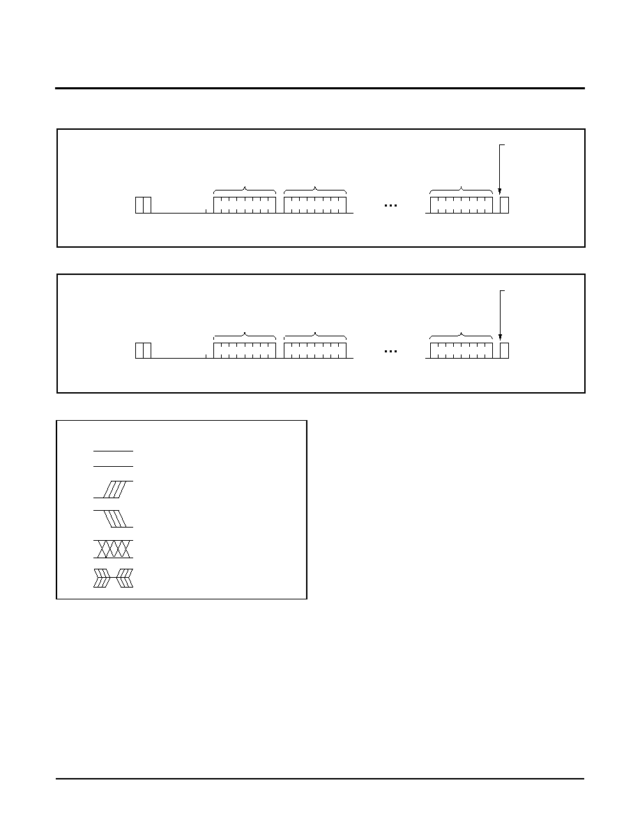
Read Password Reset
This mode allows resetting of the READ password to all
"0"s in case re-programming is needed and the old pass-
word is not known.
Write Password Reset
This mode allows resetting of the WRITE password to all
"0"s in case re-programming is needed and the old pass-
word is not known.
Mass Program
This mode allows mass programming of the array, con-
figuration registers and password to all "0"s using a spe-
cial configuration command. All parts are shipped mass
programmed.
Mass Erase
This mode allows mass erase of the array, configuration
register and password to all "1"s using a special configu-
ration command.
Figure 15. Program Configuration Registers
Figure 16. Read Configuration Registers
S
T
A
R
T
S
C M D A
X
A
X
A
X
A
X
A
8
A
C
K
CONFIGURATION
PASSWORD 7
A
C
K
A
C
K
A
C
K
A
C
K
CONFIGURATION
PASSWORD 0
WAIT
tWC/ACK POLLING
BCR 1
BYTE
A
C
K
A
C
K
S
T
O
P
SDA LINE
IF PASSWORD
MATCH THEN
S
BCR 2
BYTE
CR
BYTE
A
C
K
A
C
K
CONFIGURATION
INSTRUCTION
RC
BYTE
A
C
K
A
C
K
WAIT
tWC
RR
BYTE
7002 ILL F18.1
S
T
A
R
T
S
C M D A
X
A
X
A
X
A
X
A
8
A
C
K
CONFIGURATION
PASSWORD 7
A
C
K
A
C
K
A
C
K
A
C
K
CONFIGURATION
PASSWORD 0
WAIT
tWC/ACK POLLING
BCR 1
BYTE
A
C
K
A
C
K
S
T
O
P
SDA LINE
IF PASSWORD
MATCH THEN
S
BCR 2
BYTE
CR
BYTE
A
C
K
A
C
K
RC
BYTE
A
C
K
RR
BYTE
7002 ILL F19.1
CONFIGURATION
INSTRUCTION
X76F041
14
ABSOLUTE MAXIMUM RATINGS*
Temperature under Bias ..................... ≠65
∞
C to +135
∞
C
Storage Temperature .......................... ≠65
∞
C to +150
∞
C
Voltage on any Pin with
Respect to V
SS
..................................... ≠1V to +7V
D.C. Output Current ................................................. 5mA
Lead Temperature
(Soldering, 10 seconds) .................................300
∞
C
*COMMENT
Stresses above those listed under "Absolute Maximum
Ratings" may cause permanent damage to the device.
This is a stress rating only and the functional operation of
the device at these or any other conditions above those
listed in the operational sections of this specification is
not implied. Exposure to absolute maximum rating condi-
tions for extended periods may affect device reliability.
Figure 17. Read/Write Password Reset
Figure 18. Mass Program/Erase
SYMBOL TABLE
S
T
A
R
T
S
C M D A
X
A
X
A
X
A
X
A
8
A
C
K
CONFIGURATION
PASSWORD 7
A
C
K
A
C
K
A
C
K
A
C
K
CONFIGURATION
PASSWORD 0
WAIT
tWC
SDA LINE
CONFIGURATION
INSTRUCTION
S
S
T
O
P
7002 ILL F20.1
WAIT
tWC/ACK POLLING
S
T
A
R
T
S
C M D A
X
A
X
A
X
A
X
A
8
A
C
K
CONFIGURATION
PASSWORD 7
A
C
K
A
C
K
A
C
K
A
C
K
CONFIGURATION
PASSWORD 0
WAIT
tWC
SDA LINE
CONFIGURATION
INSTRUCTION
S
S
T
O
P
7002 ILL F20A.1
WAIT
tWC/ACK POLLING
WAVEFORM
INPUTS
OUTPUTS
Must be
steady
Will be
steady
May change
from LOW
to HIGH
Will change
from LOW
to HIGH
May change
from HIGH
to LOW
Will change
from HIGH
to LOW
Don't Care:
Changes
Allowed
Changing:
State Not
Known
N/A
Center Line
is High
Impedance
X76F041
15
RECOMMENDED OPERATING CONDITIONS
7002 FRM T05
7002 FRM T06.1
Temp
Min.
Max.
Commercial
0
∞
C
+70
∞
C
Extended
≠20
∞
C
+85
∞
C
Supply Voltage
Limits
X76F041
4.5V to 5.5V
X76F041 ≠ 3
3V to 3.6V
D.C. OPERATING CHARACTERISTICS (Over the recommended operating conditions unless otherwise specified.)
7002 FRM T07.1
CAPACITANCE T
A
= +25
∞
C, f = 1MHz, V
CC
= 5V
7002 FRM T08
NOTES: (1)
Must perform a stop command after a read command prior to measurement
(2)
V
IL
min. and V
IH
max. are for reference only and are not tested.
(3)
This parameter is periodically sampled and not 100% tested.
Symbol
Parameter
Limits
Units
Test Conditions
Min.
Max.
I
CC1
V
CC
Supply Current (Read)
2
mA
f
SCL
= V
CC
x 0.1/V
CC
x 0.9 Levels @ 1MHz,
SDA = Open
RST = CS = V
SS
I
CC2
(3)
V
CC
Supply Current (Write)
3
mA
f
SCL
= V
CC
x 0.1/V
CC
x 0.9 Levels @ 1MHz,
SDA = Open
RST = CS = V
SS
I
SB1
(1)
V
CC
Supply Current (Standby)
100
µ
A
SCL = V
SS
, CS = V
CC
≠ 0.3V
SDA = Open, RST = V
CC
= 5.5V
I
SB2
(1)
V
CC
Supply Current (Standby)
50
µ
A
SCL = V
SS
, CS = V
CC
≠ 0.3V
SDA = Open, RST = V
SS
, V
CC
= 3V
I
LI
Input Leakage Current
10
µ
A
V
IN
= V
SS
to V
CC
I
LO
Output Leakage Current
10
µ
A
V
OUT
= V
SS
to V
CC
V
IL1
(2)
Input LOW Voltage
≠0.5
V
CC
x 0.3
V
V
CC
= 5.5V
V
IH1
(2)
Input HIGH Voltage
V
CC
x 0.7 V
CC
+ 0.5
V
V
CC
= 5.5V
V
IL2
(2)
Input LOW Voltage
≠0.5
V
CC
x 0.1
V
V
CC
= 3.0V
V
IH2
(2)
Input HIGH Voltage
V
CC
x 0.9 V
CC
+ 0.5
V
V
CC
= 3.0V
V
OL
Output LOW Voltage
0.4
V
I
OL
= 2mA
V
OH
Output HIGH Voltage
V
CC
≠ 0.8
V
I
OH
= ≠1mA
Symbol
Test
Max.
Units
Conditions
C
OUT
(3)
Output Capacitance (SDA)
10
pF
V
I/O
= 0V
C
IN
(3)
Input Capacitance (RST, SCL, CS)
10
pF
V
IN
= 0V
EQUIVALENT A.C. LOAD CIRCUIT
A.C. TEST CONDITIONS
7002 FRM T09
3V
1.3K
OUTPUT
100pF
7002 ILL F21.1
5V
2.3K
OUTPUT
100pF
Input Pulse Levels
V
CC
x 0.1 to V
CC
x 0.9
Input Rise and Fall Times
10ns
Input and Output Timing Level
V
CC
x 0.5
Output Load
100pF

X76F041
16
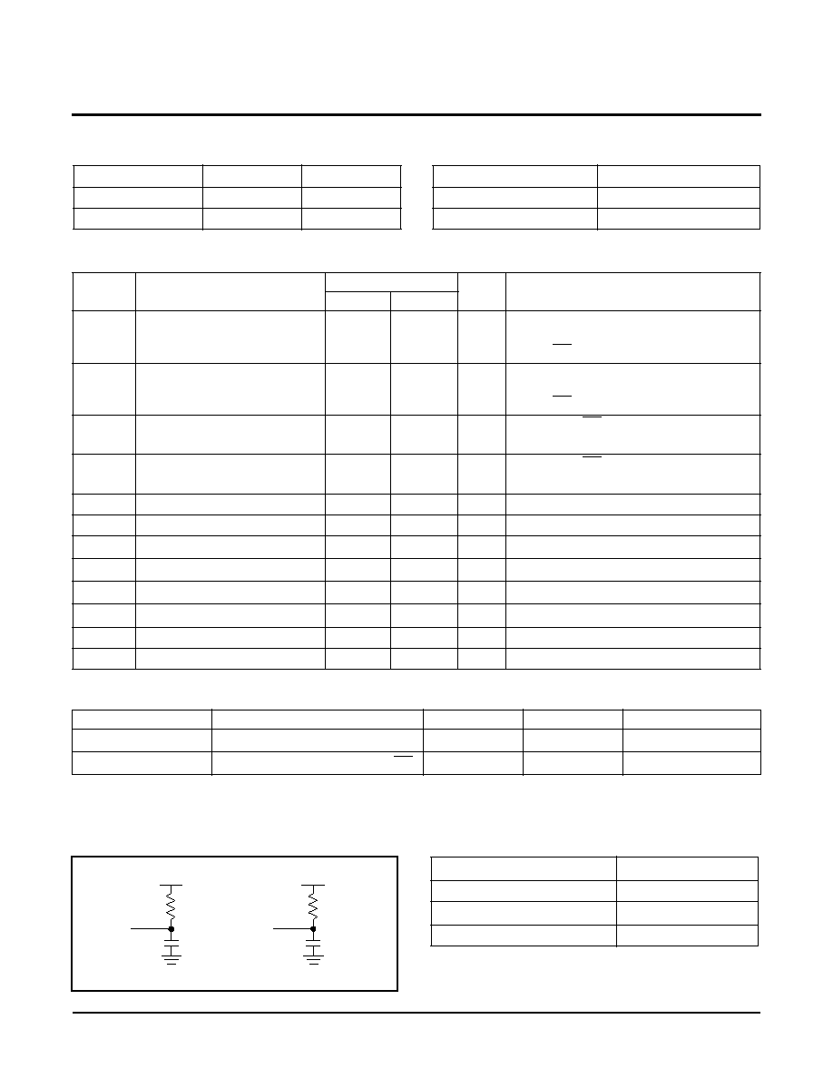
A.C. CHARACTERISTICS (Over recommended operating conditions, unless otherwise specified)
Read & Write Cycle Limits
7002 FRM T10
NOTES: (4) This parameter is periodically sampled and not 100% tested.
Symbol
Parameter
Min.
Max.
Units
f
SCL
SCL Clock Frequency
1
MHz
TI
Noise Suppression Time Constant at SCL & SDA Inputs
20
ns
t
DV
SCL HIGH to SDA Data Valid
450
ns
t
LOW
Clock LOW Period
500
ns
t
HIGH
Clock HIGH Period
500
ns
t
STAS1
Start Condition Setup Time to Rising Edge of SCL
150
ns
t
STAS2
Start Condition Setup Time to Falling Edge of SCL
150
ns
t
STAH1
Start Condition Hold Time to Rising Edge of SCL
50
ns
t
STAH2
Start Condition Hold Time to Falling Edge of SCL
50
ns
t
STPS1
Stop Condition Setup Time to Rising Edge of SCL
150
ns
t
STPS2
Stop Condition Setup Time to Falling Edge of SCL
150
ns
t
STPH1
Stop Condition Hold Time to Rising Edge of SCL
50
ns
t
STPH2
Stop Condition Hold Time to Falling Edge of SCL
50
ns
t
HD:DAT
Data in Hold Time
10
ns
t
SU:DAT
Data in Setup Time
150
ns
t
RSCL
(4)
SCL Rise Time
90
ns
t
FSCL
(4)
SCL Fall Time
90
ns
t
R
(4)
SDA, CS, RST Rise Time
90
ns
t
F
(4)
SDA, CS, RST Fall Time
90
ns
t
DH
Data Out Hold Time
0
ns
t
HZ1
SCL LOW to High Impedance
150
ns
t
LZ
SCL HIGH to Output Active
0
ns
t
VCCS
V
CC
to CS Setup Time
5
ms
t
SU:CS
CS Setup Time
200
ns
t
HD:CS
CS Hold Time
100
ns
t
HZ2
CS Deselect Time
150
ns
t
SU:SCL
SCL Setup Time to CS LOW after Power Up
200
ns
t
RST
RST HIGH Time
1500
ns
t
SU:RST
RST Setup Time
500
ns
f
SCL:RST
SCL Frequency During Response to Reset
1
MHz
t
LOW:RST
SCL LOW Time During Response to Reset
500
ns
t
HIGH:RST
SCL HIGH Time During Response to Reset
500
ns
t
PD
SCL LOW to SDA Valid During Response to Reset
450
ns
t
NOL
RST to SCL Non-Overlap
500
ns
t
WC
Nonvolatile Write Cycle
10
ms

X76F041
17
Bus Timing
(1)
-- SDA Driven by the Bus Master
Bus Timing
(2)
-- SDA Driven by the Slave
START Condition Timing
NOTES: (1)
The master may issue a STOP condition at any given time in which it is driving the SDA line. In other words, when the part is sending
ACK or data the master may NOT issue a STOP condition. The part will not respond to any such attempt which also causes bus con-
tention. At any other time, a STOP condition will cause the part to reset and stop (enter a stand-by mode). Write operations will termi-
nate prior to entering the stand-by mode.
(2)
When the part drives the SDA line, it will tri-state the bus only after the last bit of the sequence. In other words, after the 8th bit of a byte
that is read or after ACK between incoming bytes. In all other cases when the part drives the bus (between successive bits) it will con-
tinue to drive the bus also during the clock LOW periods.
SCL
SDA (IN)
from master
tFSCL
tRSCL
tLOW
tHIGH
tSU:DAT
tHD:DAT
tF
tR
Start
bit
7002 ILL F22
1st clock
pulse of
sequence
tDH
tDV
tLZ
tHZ1
7002 ILL F23
last clock
pulse of
sequence
SCL
SDA (OUT)
from slave
SCL
tSTAS1
tSTAH1
tSTAS2
tSTAH2
Start Bit
7002 ILL F24
SDA (IN)
from master
X76F041
18
STOP Condition Timing
Acknowledge Response from Slave (Same Timing as Data Out)
Acknowledge Response from Master
CS Timing Diagram (Selecting/Deselecting the Part)
SCL
tSTPS1
tSTPH1
tSTPS2
tSTPH2
Stop Bit
7002 ILL F25
SDA (IN)
from master
SCL
SDA (OUT)
from slave
(acknowledge)
tLZ
tDV
tDH
tHZ1
7002 ILL F26
SCL
SDA (OUT)
from master
(acknowledge)
tSU:DAT
tHD:DAT
7002 ILL F27
SCL
tSU:CS
tHD:CS
CS
from
master
7002 ILL F28
X76F041
19
V
CC
to CS Setup Timing Diagram
CS Deselect
RST Timing Diagram -- Response to a Synchronous Reset (ISO)
NOTES: (1)
The reset operation results in an answer from the part containing a header transmitted from the part to the master. The header has a
fixed length of 32 bits and begins with two mandatory fields of eight bits : H1 and H2.
(2)
The chronological order of transmission of the information bits shall correspond to bit identification b1 to b32 with the LEAST
significant bit transmitted first.
(3)
The current values are:
H1 : 19 h
H2 : 55 h
H3 : AA h
H4 : 55 h
VCC
CS
tSU:SCL
VCCMIN
tSU:CS
SCL
tVCCS
7002 ILL F29
CS
SDA (OUT)
from slave
tHZ2
7002 ILL F29A
SCL
SDA
tNOL
tPD
(low)
1st DATA BIT
2nd DATA BIT
CS
RST
tRST
1st
clk.
pulse
2nd
clk.
pulse
3rd
clk.
pulse
tSU:RST
tHIGH_RST
fSCL_RST
tLOW_RST
tPD
7002 ILL F30
X76F041
20
NOTE:
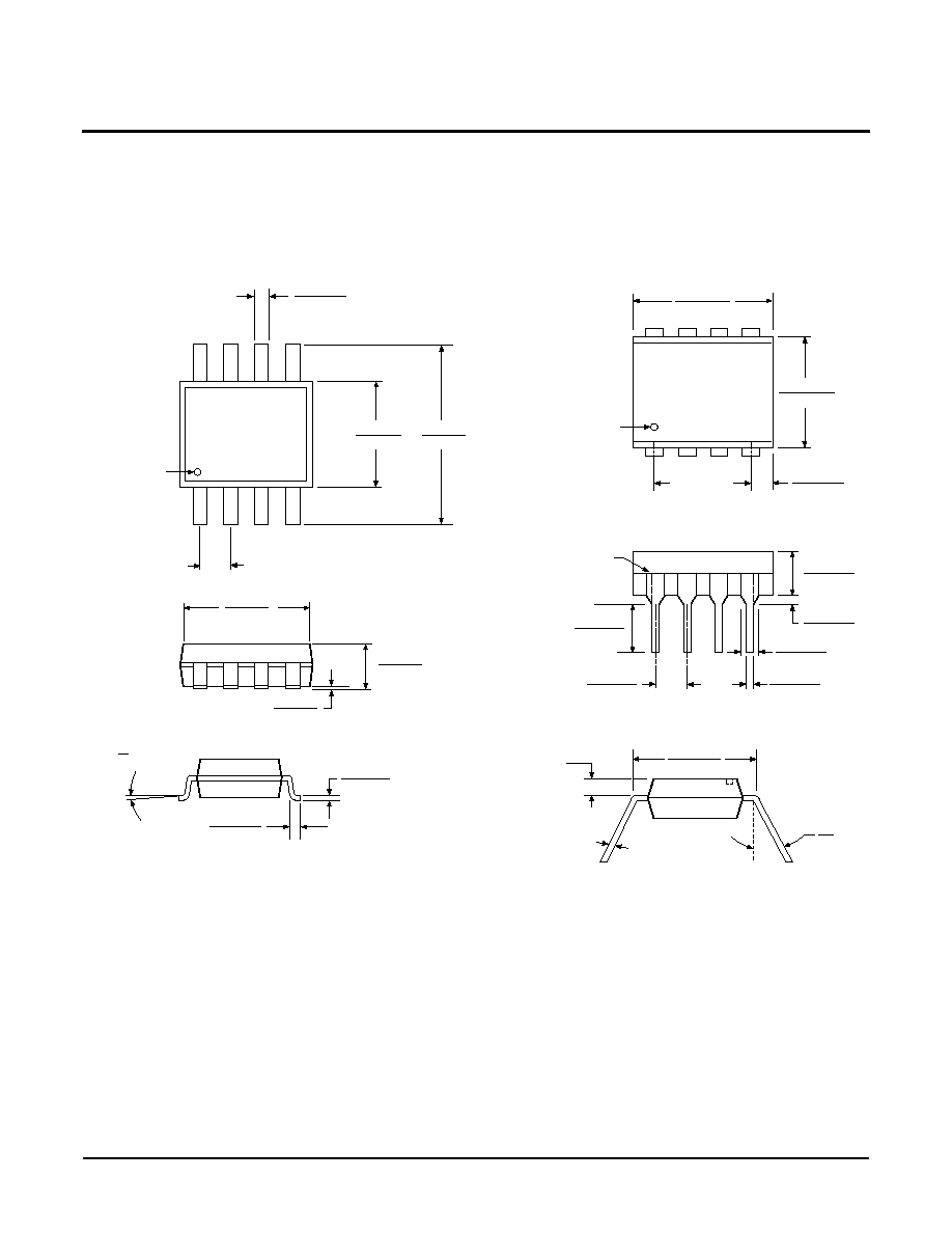
1. ALL DIMENSIONS IN INCHES (IN PARENTHESES IN MILLIMETERS)
2. PACKAGE DIMENSIONS EXCLUDE MOLDING FLASH
0.020 (.508)
0.012 (.305)
.080 (2.03)
.070 (1.78)
.213 (5.41)
.205 (5.21)
0
8
.330 (8.38)
.300 (7.62)
.212 (5.38)
.203 (5.16)
.035 (.889)
.020 (.508)
.010 (.254)
.007 (.178)
REF
PIN 1 ID
.050 (1.27) BSC
8-LEAD PLASTIC, 0.200" WIDE SMALL OUTLINE
GULLWING PACKAGE TYP "A" (EIAJ SOIC)
.013 (.330)
.004 (.102)
3926 ILL F33.1
PACKAGING INFORMATION
3926 FHD F01
NOTE:
1. ALL DIMENSIONS IN INCHES (IN PARENTHESES IN MILLIMETERS)
2. PACKAGE DIMENSIONS EXCLUDE MOLDING FLASH
0.020 (0.51)
0.016 (0.41)
0.150 (3.81)
0.125 (3.18)
0.110 (2.79)
0.090 (2.29)
0.430 (10.92)
0.360 (9.14)
0.300
(7.62) REF.
PIN 1 INDEX
0.145 (3.68)
0.128 (3.25)
0.025 (0.64)
0.015 (0.38)
PIN 1
SEATING
PLANE
0.065 (1.65)
0.045 (1.14)
0.260 (6.60)
0.240 (6.10)
0.060 (1.52)
0.020 (0.51)
TYP. 0.010 (0.25)
0
∞
15
∞
8-LEAD PLASTIC DUAL IN-LINE PACKAGE TYPE P
HALF SHOULDER WIDTH ON
ALL END PINS OPTIONAL
0.015 (0.38)
MAX.
0.325 (8.25)
0.300 (7.62)

X76F041
21
X76F041
X
X
≠X
ORDERING INFORMATION
V
CC
Limits
Blank = 5V
±
10%
3 = 3V to 3.6V
Temperature Range
Blank = Commercial = 0
∞
C to +70
∞
C
E = Extended = ≠20
∞
C to +85
∞
C
Package
P = 8-Lead Plastic DIP
A = 8-Lead SOIC (EIAJ)
H = Die in Waffle Packs
W = Die in Wafer Form
Device
LIMITED WARRANTY
Devices sold by Xicor, Inc. are covered by the warranty and patent indemnification provisions appearing in its Terms of Sale only. Xicor, Inc. makes no warranty,
express, statutory, implied, or by description regarding the information set forth herein or regarding the freedom of the described devices from patent infringement.
Xicor, Inc. makes no warranty of merchantability or fitness for any purpose. Xicor, Inc. reserves the right to discontinue production and change specifications and
prices at any time and without notice.
Xicor, Inc. assumes no responsibility for the use of any circuitry other than circuitry embodied in a Xicor, Inc. product. No other circuits, patents, licenses are implied.
U.S. PATENTS
Xicor products are covered by one or more of the following U.S. Patents: 4,263,664; 4,274,012; 4,300,212; 4,314,265; 4,326,134; 4,393,481; 4,404,475;
4,450,402; 4,486,769; 4,488,060; 4,520,461; 4,533,846; 4,599,706; 4,617,652; 4,668,932; 4,752,912; 4,829, 482; 4,874, 967; 4,883, 976. Foreign patents and
additional patents pending.
LIFE RELATED POLICY
In situations where semiconductor component failure may endanger life, system designers using this product should design the system with appropriate error detec-
tion and correction, redundancy and back-up features to prevent such an occurence.
Xicor's products are not authorized for use in critical components in life support devices or systems.
1. Life support devices or systems are devices or systems which, (a) are intended for surgical implant into the body, or (b) support or sustain life, and whose failure
to perform, when properly used in accordance with instructions for use provided in the labeling, can be reasonably expected to result in a significant injury to the
user.
2. A critical component is any component of a life support device or system whose failure to perform can be reasonably expected to cause the failure of the life sup-
port device or system, or to affect its safety or effectiveness.