 | –≠–ª–µ–∫—Ç—Ä–æ–Ω–Ω—ã–π –∫–æ–º–ø–æ–Ω–µ–Ω—Ç: X76F101-3 | –°–∫–∞—á–∞—Ç—å:  PDF PDF  ZIP ZIP |
©
Xicor, Inc. 1994, 1995, 1996 Patents Pending
7065 -1.1 4/17/98 T2/C0/D0 SH
1
Characteristics subject to change without notice
1K
X76F101
128 x 8 bit
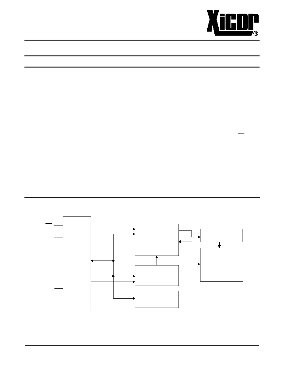
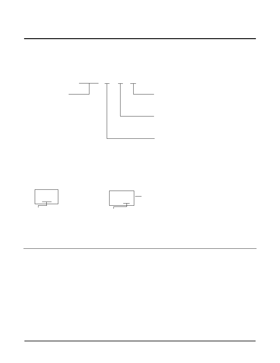
Functional Diagram
Secure SerialFlash
FEATURES
∑ 64-bit Password Security
∑ One Array (112 Bytes) Two Passwords
--Read Password
--Write Password
∑ Programmable Passwords
∑ 32-bit Response to Reset (RST Input)
∑ 8 byte Sector Write mode
∑ 1MHz Clock Rate
∑ 2 wire Serial Interface
∑ Low Power CMOS
--3.0 to 5.5V operation
--Standby current Less than 1µA
--Active current less than 3 mA
∑ High Reliability Endurance:
--100,000 Write Cycles
∑ Data Retention: 100 years
∑ Available in:
--8 lead PDIP, SOIC, MSOP and ISO Card
--SmartCard Module
DESCRIPTION
The X76F101 is a Password Access Security Supervisor,
containing one 896-bit Secure SerialFlash array. Access
to the memory array can be controlled by two 64-bit
passwords. These passwords protect read and write
operations of the memory array.
The X76F101 features a serial interface and software
protocol allowing operation on a popular two wire bus.
The bus signals are a clock Input (SCL) and a
bidirectional data input and output (SDA). Access to the
device is controlled through a chip select (CS) input,
allowing any number of devices to share the same bus.
The X76F101 also features a synchronous response to
reset providing an automatic output of a hard-wired 32-bit
data stream conforming to the industry standard for
memory cards.
The X76F101 utilizes Xicor's proprietary Direct Write
TM
cell, providing a minimum endurance of 100,000 cycles
and a minimum data retention of 100 years.
LOGIC
CS
SCL
SDA
RST
INTERFACE
8K BYTE
DATA TRANSFER
ARRAY ACCESS
ENABLE
RESET
RESPONSE REGISTER
PASSWORD ARRAY
AND PASSWORD
VERIFICATION LOGIC
CHIP ENABLE
RETRY COUNTER
SerialFlash ARRAY
32 BYTE
SerialFlash ARRAY
ARRAY 0
ARRAY 1
(PASSWORD PROTECTED)
(PASSWORD PROTECTED)
7025 FM 01
Logic
SCL
SDA
RST
Interface
112 Byte
Data Transfer
Array Access
Enable
ISO Reset
Response Register
Password Array
and Password
Verification Logic
Chip Enable
Erase Logic
EEPROM Array
CS
X76F101
2
PIN DESCRIPTIONS
Serial Clock (SCL)
The SCL input is used to clock all data into and out of the
device.
Serial Data (SDA)
SDA is an open drain serial data input/output pin. During
a read cycle, data is shifted out on this pin. During a write
cycle, data is shifted in on this pin. In all other cases, this
pin is in a high impedance state.
Chip Select (CS)
When CS is high, the X76F101 is deselected and the
SDA pin is at high impedance and unless an internal
write operation is underway, the X76F101 will be in
standby mode. CS low enables the X76F101, placing it in
the active mode.
Reset (RST)
RST is a device reset pin. When RST is pulsed high
while CS is low the X76F101 will output 32 bits of fixed
data which conforms to the standard for "synchronous
response to reset". CS must remain LOW and the part
must not be in a write cycle for the response to reset to
occur. See Figure 7. If at any time during the response to
reset CS goes HIGH, the response to reset will be
aborted and the part will return to the standby state. The
response to reset is "mask programmable" only!
DEVICE OPERATION
The X76F101 memory array consists of fourteen 8-byte
sectors. Read or write access to the array always begins
at the first address of the sector. Read operations then
can continue indefinitely. Write operations must total 8
bytes.
There are two primary modes of operation for the
X76F101; Protected READ and protected WRITE.
Protected operations must be performed with one of two
8-byte passwords.
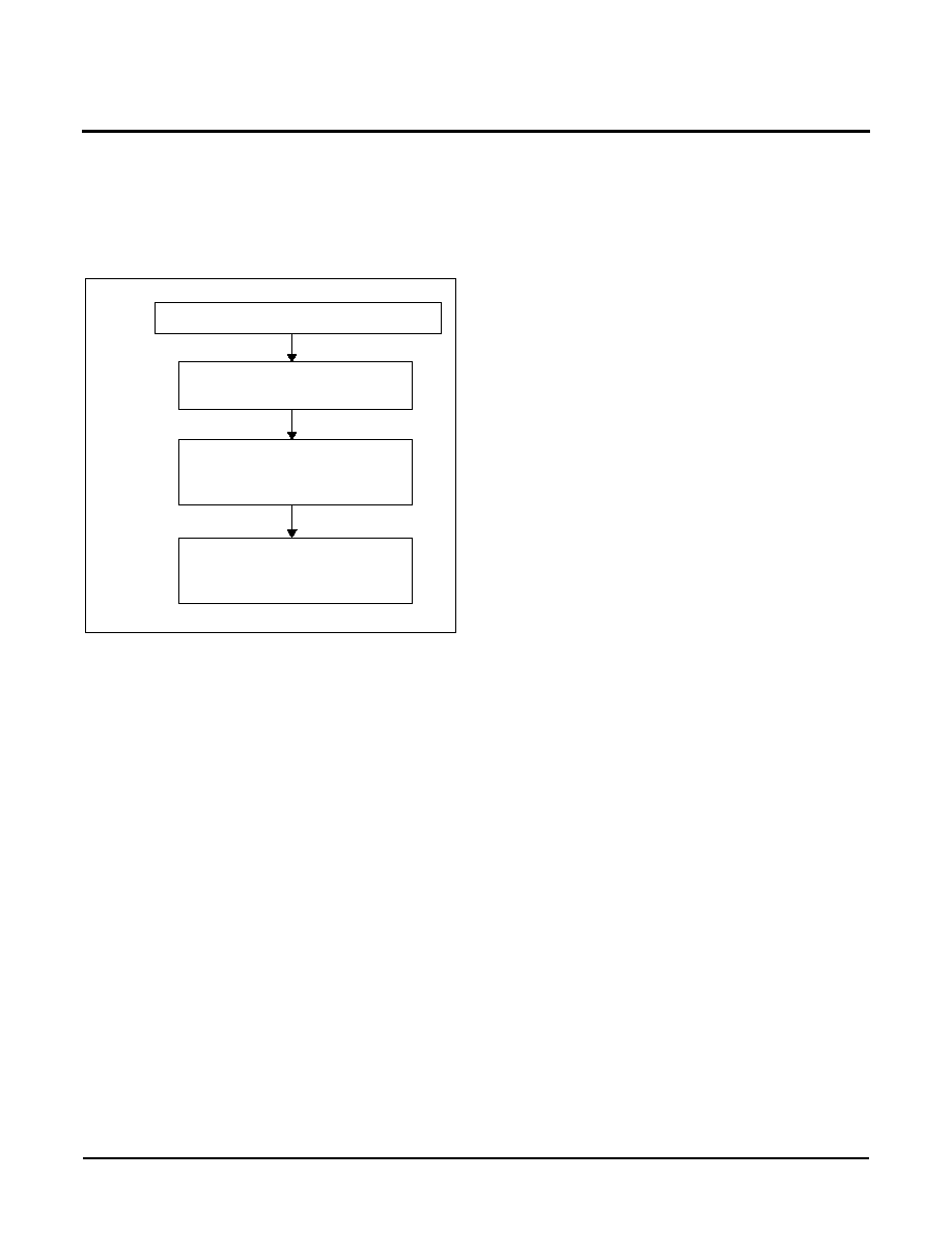
The basic method of communication for the device is
established by first enabling the device (CS LOW),
generating a start condition, then transmitting a
command, followed by the correct password. All parts will
be shipped from the factory with all passwords equal to
`0'. The user must perform ACK Polling to determine the
validity of the password, before starting a data transfer
(see Acknowledge Polling.) Only after the correct
password is accepted and a ACK polling has been
performed, can the data transfer occur.
To ensure the correct communication, RST must remain
LOW under all conditions except when running a
"Response to Reset sequence".
Data is transferred in 8-bit segments, with each transfer
being followed by an ACK, generated by the receiving
device.
If the X76F101 is in a nonvolatile write cycle a "no ACK"
(SDA=High) response will be issued in response to
loading of the command byte. If a stop is issued prior to
the nonvolatile write cycle the write operation will be
terminated and the part will reset and enter into a
standby mode.
The basic sequence is illustrated in Figure 1.
PIN NAMES
PIN CONFIGURATION
Symbol
Description
CS
Chip Select Input
SDA
Serial Data Input/Output
SCL
Serial Clock Input
RST
Reset Input
Vcc
Supply Voltage
Vss
Ground
NC
No Connect
CS
SDA
V
CC
RST
SCL
NC
1
2
3
4
7
8
6
5
SOIC
V
CC
RST
SCL
V
SS
NC
SDA
Smart Card
CS
NC
NC
GND
CS
SDA
VCC
RST
SCL
NC
1
2
3
4
7
8
6
5
MSOP
VSS
NC
NC
RST
SCL
SDA
Vss
1
2
3
4
7
8
6
5
PDIP
V
CC
CS
NC
X76F101
3
After each transaction is completed, the X76F101 will
reset and enter into a standby mode. This will also be the
response if an unsuccessful attempt is made to access a
protected array.
Figure 1. X76F101 Device Operation
Device Protocol
The X76F101 supports a bidirectional bus oriented
protocol.
The protocol defines any device that sends data
onto the bus as a transmitter and the receiving device as
a receiver. The device controlling the transfer is a master
and the device being controlled is the slave. The master
will always initiate data transfers and provide the clock for
both transmit and receive operations. Therefore, the
X76F101 will be considered a slave in all applications.
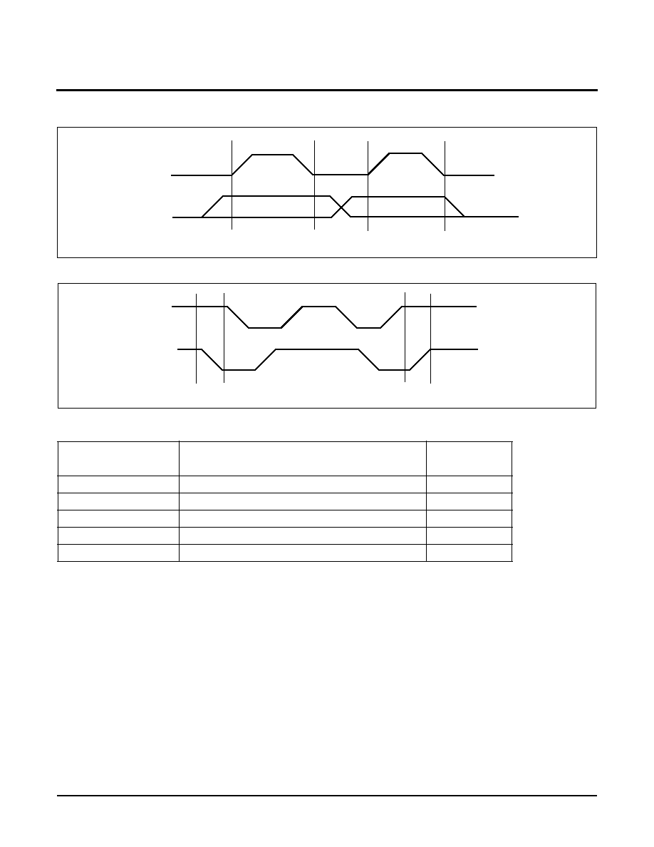
Clock and Data Conventions
Data states on the SDA line can change only during SCL
LOW. SDA changes during SCL HIGH are reserved for
indicating start and stop conditions. Refer to Figure 2 and
Figure 3.
Start Condition
All commands are preceeded by the start condition,
which is a HIGH to LOW transition of SDA when SCL is
HIGH. The X76F101 continuously monitors the SDA and
SCL lines for the start condition and will not respond to
any command until this condition is met.
A start may be issued to terminate the input of a control
byte or the input data to be written. This will reset the
device and leave it ready to begin a new read or write
command. Because of the push/pull output, a start
cannot be generated while the part is outputting data.
Starts are inhibited while a write is in progress.
Stop Condition
All communications must be terminated by a stop
condition.
The stop condition is a LOW to HIGH transition
of SDA when SCL is HIGH. The stop condition is also
used to reset the device during a command or data input
sequence and will leave the device in the standby power
mode. As with starts, stops are inhibited when outputting
data and while a write is in progress.
Acknowledge
Acknowledge is a software convention used to indicate
successful data transfer. The transmitting device, either
master or slave, will release the bus after transmitting
eight bits. During the ninth clock cycle the receiver will
pull the SDA line LOW to acknowledge that it received
the eight bits of data.
The X76F101 will respond with an acknowledge after
recognition of a start condition and its slave address. If
both the device and a write condition have been
selected, the X76F101 will respond with an acknowledge
after the receipt of each subsequent eight-bit word.
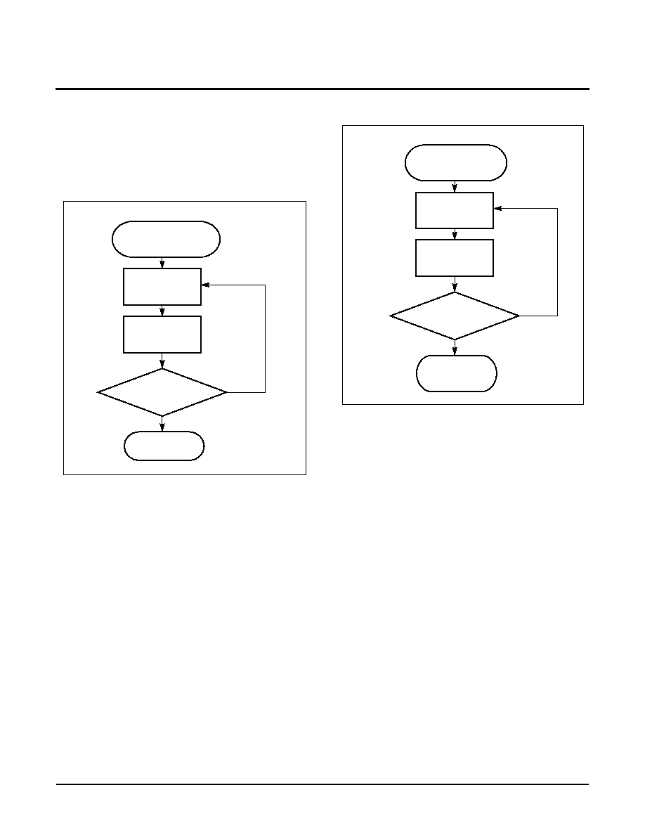
LOAD COMMAND/ADDRESS BYTE
LOAD 8-BYTE
PASSWORD
VERIFY PASSWORD
ACCEPTANCE BY
USE OF ACK POLLING
READ/WRITE
DATA
BYTES
X76F101
4
Figure 2. Data Validity
Figure 3. Definition of Start and Stop Conditions
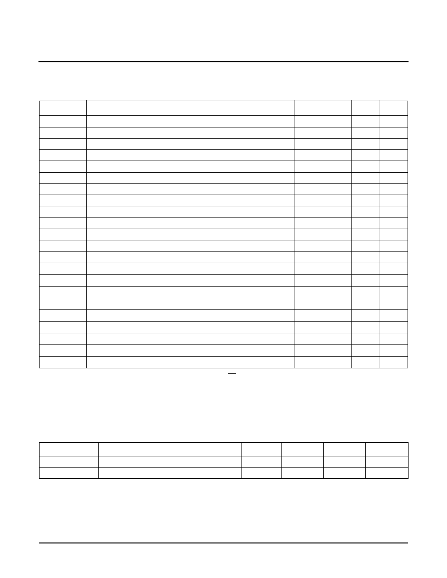
Table 1. X76F101 Instruction Set
Illegal command codes will be disregarded. The part will respond with a "no-ACK" to the illegal byte and then return to
the standby mode. All write/read operations require a password.
Command
after Start
Command Description
Password
used
1 0 0 S
3
S
2
S
1
S
0
0
Sector Write
Write
1 0 0 S
3
S
2
S
1
S
0
1
Sector Read
Read
1 1 1 1 1 1 0 0
Change Write Password
Write
1 1 1 1 1 1 1 0
Change Read Password
Write
0 1 0 1 0 1 0 1
Password ACK Command
None
SCL
SDA
Data Stable
Data
Change
SCL
SDA
Start Condition
Stop Condition
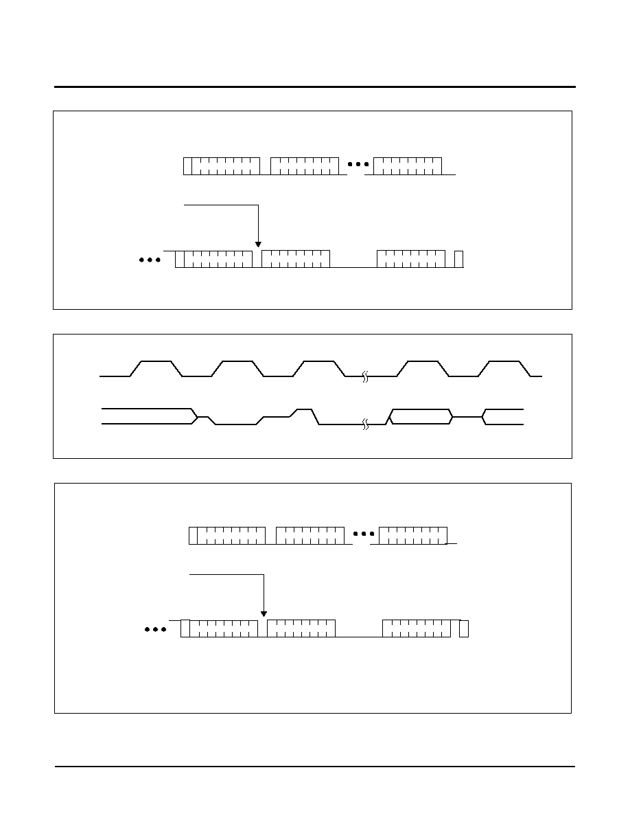
PROGRAM OPERATIONS
Sector Write
The sector write mode requires issuing the 8-bit write
command followed by the password and then the data
bytes transferred as illustrated in figure 4. The write
command byte contains the address of the sector to be
written. Data is written starting at the first address of a
sector and eight bytes must be transferred. After the last
byte to be transferred is acknowledged a stop condition is
issued which starts the nonvolatile write cycle. If more or
less than 8 bytes are transferred, the data in the sector
remains unchanged.
ACK Polling
Once a stop condition is issued to indicate the end of the
host's write sequence, the X76F101 initiates the internal
nonvolatile write cycle. In order to take advantage of the
typical 5ms write cycle, ACK polling can begin
immediately. This involves issuing the start condition
X76F101
5
followed by the new command code of 8 bits (1st byte of
the protocol.) If the X76F101 is still busy with the
nonvolatile write operation, it will issue a "no-ACK" in
response. If the nonvolatile write operation has
completed, an "ACK" will be returned and the host can
then proceed with the rest of the protocol.
After the password sequence, there is always a nonvola-
tile write cycle. This is done to discourage random
guesses of the password if the device is being tampered
with. In order to continue the transaction, the X76F101
requires the master to perform a password ACK polling
sequence with the specific command code of 55h. As
with regular Acknowledge polling the user can either time
out for 10ms, and then issue the ACK polling once, or
continuously loop as described in the flow.
If the password that was inserted was correct, then an
"ACK" will be returned once the nonvolatile cycle in
response to the passwrod ACK polling sequence is over.
If the password that was inserted was incorrect, then a
"no ACK" will be returned even if the nonvolatile cycle is
over. Therefore, the user cannot be certain that the pass-
word is incorrect until the 10ms write cycle time has
elapsed.
READ OPERATIONS
Read operations are initiated in the same manner as
write operations but with a different command code.
Sector Read
With sector read, a sector address is supplied with the
read command. Once the password has been
acknowledged data may be read from the sector. An
acknowledge must follow each 8-bit data transfer. A read
operation always begins at the first byte in the sector, but
may stop at any time. Random accesses to the array are
not possible. Continuous reading from the array will
return data from successive sectors. After reading the
last sector in the array, the address is automatically set to
the first sector in the array and data can continue to be
read out. After the last bit has been read, a stop condition
is generated without sending a preceding acknowledge.
Data ACK Polling Sequence
ACK
RETURNED
?
ISSUE NEW
COMMAND
CODE
WRITE SEQUENCE
COMPLETED
ENTER ACK POLLING
ISSUE START
NO
YES
PROCEED
Password ACK Polling Sequence
ACK
RETURNED
?
ISSUE
PASSWORD
ACK COMMAND
PASSWORD LOAD
COMPLETED
ENTER ACK POLLING
ISSUE START
NO
YES
PROCEED
X76F101
6
Figure 4. Sector Write Sequence (Password Required)
Figure 5. Acknowledge Polling
Figure 6. Sector Read Sequence (Password Required)
A
CK
ST
AR
T
WRITE
A
CK
A
CK
A
CK
A
CK
Write
Password
7
Write
Password
0
A
CK
S
SDA
. . .
Wait t
WC
OR
ACK
Password
Command
ST
AR
T
Password ACK
A
CK
S
COMMAND
no-A
CK
If ACK, Then
Password Matches
COMMAND
ST
OP
Host
Commands
Host
Commands
X76F101
Responce
X76F101
Response
A
CK
A
CK
A
CK
Wait t
WC
Data ACK Polling
P
8th clk.
of 8th
pwd. byte
`ACK'
clk
8th
clk
`ACK'
clk
`ACK'
START
condition
8th bit
ACK or
no ACK
SCL
SDA
Data n
A
CK
ST
AR
T
READ
A
CK
A
CK
A
CK
A
CK
Read
Password
7
Read
Password
0
A
CK
Data 0
S
SDA
. . .
Wait t
WC
OR
ACK
Password
Command
ST
AR
T
Password ACK
A
CK
S
COMMAND
no-A
CK
If ACK, Then
Password Matches
COMMAND
ST
OP
Host
Commands
Host
Commands
X76F101
Responce
X76F101
Response
P
X76F101
7
PASSWORDS
Passwords are changed by sending the "change read
password" or "change write password" commands in a
normal sector write operation. A full eight bytes
containing the new password must be sent, following
successful transmission of the current write password
and a valid password ACK response. The user can use a
repeated ACK Polling command to check that a new
password has been written correctly. An ACK indicates
that the new password is valid.
There is no way to read any of the passwords.
RESPONSE TO RESET (DEFAULT = 19 01 AA 55)
The ISO Response to reset is controlled by the RST, CS
and CLK pins. When RST is pulsed high, while CS is low,
the device will output 32 bits of data, one bit per clock.
This conforms to the ISO standard for "synchronous
response to reset". CS must remain LOW and the part
must not be in a write cycle for the response to reset to
occur.
After initiating a nonvolatile write cycle the RST pin must
not be pulsed until the nonvolatile write cycle is complete.
If not, the ISO response will not be activated. Also, any
attempt to pulse the RST pin in the middle of an ISO
transaction will stop the transaction with the SDA pin in
high impedance. The user will have to issue a stop
condition and start the transaction again. If at any time
during the Response to Reset CS goes HIGH, the
response to reset will be aborted and the part will return
to the standby state. A Response to Reset is not
available during a nonvolatile write cycle.
Continued clocks after the 32 bits, will output the 32 bit
sequence again, starting at byte 0.
Figure 7. Response to RESET (RST)
CS
SCK
SO
RST
Byte
0
MSB
LSB
LSB
MSB
1
LSB
MSB LSB
MSB
2
3
ABSOLUTE MAXIMUM RATINGS*
Temperature under Bias ..................... ≠65∞C to +135∞C
Storage Temperature ..........................≠65∞C to +150∞C
Voltage on any Pin with
Respect to V
SS
.......................................≠1V to +7V
D.C. Output Current..................................................5mA
Lead Temperature
(Soldering, 10 seconds).................................. 300∞C
*COMMENT
Stresses above those listed under "Absolute Maximum
Ratings" may cause permanent damage to the device.
This is a stress rating only and the functional operation of
the device at these or any other conditions above those
listed in the operational sections of this specification is
not implied. Exposure to absolute maximum rating
conditions for extended periods may affect device
reliability.
X76F101
8
RECOMMENDED OPERATING CONDITIONS
Temp
Min.
Max.
Commercial
0∞C
+70∞C
Industrial
≠40∞C
+85∞C
Supply Voltage
Limits
X76F101
4.5V to 5.5V
X76F101 ≠ 3
3.0V to 5.5V
D.C. OPERATING CHARACTERISTICS
(Over the recommended operating conditions unless otherwise specified.)
CAPACITANCE
T
A
= +25∞C, f = 1MHz, V
CC
= 5V
NOTES:
(1)
Must perform a stop command after a read command prior to measurement
(2)
V
IL
min. and V
IH
max. are for reference only and are not tested.
(3)
This parameter is periodically sampled and not 100% tested.
Symbol
Parameter
Limits
Units
Test Conditions
Min.
Max.
I
CC1
V
CC
Supply Current
(Read)
1
mA
f
SCL
= V
CC
x 0.1/V
CC
x 0.9 Levels @ 400 KHz,
SDA = Open
RST = CS = V
SS
I
CC2
(3)
V
CC
Supply Current
(Write)
3
mA
f
SCL
= V
CC
x 0.1/V
CC
x 0.9 Levels @ 400 KHz,
SDA = Open
RST = CS = V
SS
I
SB1
(1)
V
CC
Supply Current
(Standby)
1
µA
V
IL
= V
CC
x 0.1, V
IH
= V
CC
x 0.9
f
SCL
= 400 KHz, f
SDA
= 400 KHz
I
SB2
(1)
V
CC
Supply Current
(Standby)
1
µA
V
SDA
= V
SCC
= V
CC
Other = GND or V
CC
≠0.3V
I
LI
Input Leakage Current
10
µA
V
IN
= V
SS
to V
CC
I
LO
Output Leakage Current
10
µA
V
OUT
= V
SS
to V
CC
V
IL
(2)
Input LOW Voltage
≠0.5
V
CC
x 0.3
V
V
IH
(2)
Input HIGH Voltage
V
CC
x 0.7 V
CC
+ 0.5
V
V
OL
Output LOW Voltage
0.4
V
I
OL
= 3mA
Symbol
Test
Max.
Units
Conditions
C
OUT
(3)
Output Capacitance (SDA)
8
pF
V
I/O
= 0V
C
IN
(3)
Input Capacitance (RST, SCL, CS)
6
pF
V
IN
= 0V
EQUIVALENT A.C. LOAD CIRCUIT
A.C. TEST CONDITIONS
3V
1.3K
OUTPUT
100pF
5V
1.53K
OUTPUT
100pF
Input Pulse Levels
V
CC
x 0.1 to V
CC
x 0.9
Input Rise and Fall Times
10ns
Input and Output Timing Level
V
CC
x 0.5
Output Load
100pF
X76F101
9
AC CHARACTERISTICS
(T
A
= -40∞C to +85∞C, V
CC
= +3.0V to +5.5V, unless otherwise specified.)
Notes: 1.
These Specs are not defined in the ISO 7816-3 Standard, since CS is not defined.
2.
C
b
= total capacitance of one bus line in pF
3.
t
AA
= 1.1µs Max below V
CC
= 3.0V.
RESET AC SPECIFICATIONS
Power Up Timing
Notes: 1.
Delays are measured from the time V
CC
is stable until the specified operation can be initiated. These parameters are periodically sampled
and not 100% tested.
2.
Typical values are for T
A
= 25∞C and V
CC
= 5.0V
Symbol
Parameter
Min
Max
Units
f
SCL
SCL Clock Frequency
0
1
MHz
t
AA
(3)
SCL LOW to SDA Data Out Valid
0.1
0.9
µ
s
t
BUF
Time the Bus Must Be Free Before a New Transmission Can Start
1.2
µ
s
t
HD:STA
Start Condition Hold Time
0.6
µ
s
t
LOW
Clock LOW Period
1.2
µ
s
t
HIGH
Clock HIGH Period
0.6
µ
s
t
SU:STA
Start Condition Setup Time (for a Repeated Start Condition)
0.6
µ
s
t
HD:DAT
Data In Hold Time
0
µ
s
t
SU:DAT
Data In Setup Time
100
ns
t
R
SDA and SCL Rise Time
20+0.1XC
b
(2)
300
ns
t
F
SDA and SCL Fall Time
20+0.1XC
b
(2)
300
ns
t
SU:STO
Stop Condition Setup Time
0.6
µ
s
t
DH
Data Out Hold Time
0.1
µ
s
t
NOL
RST to SCL Non-Overlap
500
ns
t
RDV
RST LOW to SDA Valid During Response to Reset
0
450
ns
t
CDV
CLK LOW to SDA Valid During Response to Reset
0
450
ns
t
DHZ
(1)
Device Deselect to SDA high impedance
0
450
ns
t
SR
(1)
Device Select to RST active
0
ns
t
RST
RST High Time
1.5
µ
s
t
SU:RST
RST Setup Time
500
ns
t
SU:CS
CS
Setup Time
200
ns
t
SU:CS
CS
Hold Time
100
ns
Symbol
Parameter
Min.
Typ
(2)
Max.
Units
t
PUR
(1)
Time from Power Up to Read
1
mS
t
PUW
(1)
Time from Power Up to Write
5
mS
X76F101
10
Nonvolatile Write Cycle Timing
Notes: 1.
t
WC
is the time from a valid stop condition at the end of a write sequence to the end of the self-timed internal nonvolatile write cycle.
It is the minimum cycle time to be allowed for any nonvolatile write by the user, unless Acknowledge Polling is used.
BUS TIMING
Write Cycle Timing
CS Timing Diagram (Selecting/Deselecting the Part)
Symbol
Parameter
Min.
Typ.(1)
Max.
Units
t
WC
(1)
Write Cycle Time
5
10
mS
tSU:STA
t HD:STA
tHD:DAT
t SU:DAT
tLOW
t SU:STO
t R
t BUF
SCL
SDA IN
SDA OUT
t DH
tAA
tF
tHIGH
SCL
SDA
t
WC
8th bit of last byte
ACK
Stop
Condition
Start
Condition
t
SU:CS
t
HD:CS
SCL
CS
from
master
X76F101
11
RST Timing Diagram ≠ Response to a Synchronous Reset
GUIDELINES FOR CALCULATING TYPICAL VALUES OF BUS PULL UP RESISTORS
t
RST
t
NOL
t
HIGH_RST
t
LOW_RST
t
CDV
t
RDV
t
SU:RST
DATA BIT (1)
DATA BIT (2)
1st
clk
pulse
2nd
clk
pulse
3rd
clk
pulse
CS
I/O
CLK
RST
t
NOL
t
SR
DATA BIT (N)
DATA BIT (N+1)
CS
I/O
CLK
RST
t
DHZ
(N+2)
100
80
60
40
20
Bus capacitance in pF
Pull Up Resistance in K
R
MIN
R
MAX
20
40
60
80
100
R
MIN
V
CCMAX
I
OLMIN
--------------------------
1.8
K
=
=
R
MAX
t
R
C
BUS
------------------
=
t
R
= maximum allowable SDA rise time
X76F101
12
NOTE:
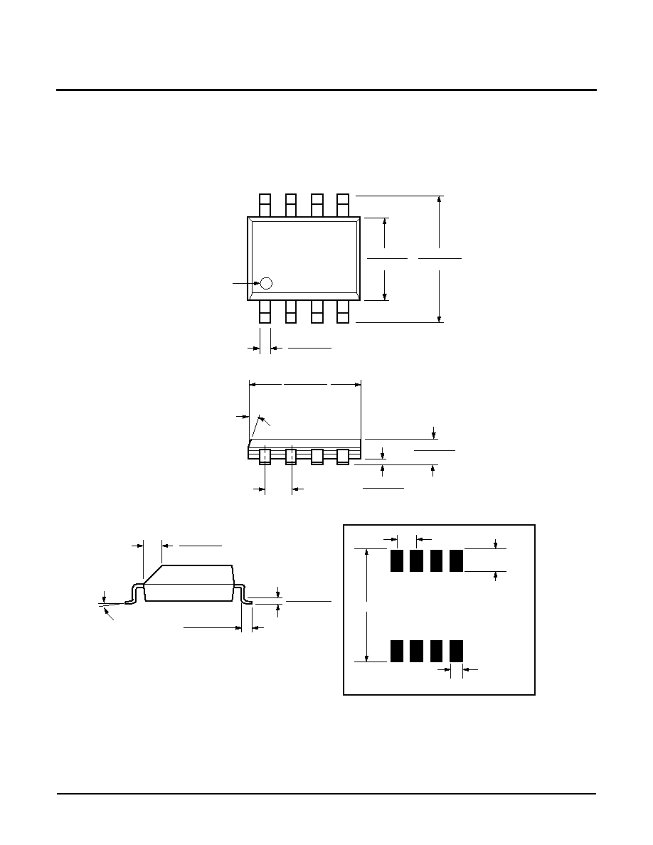
1. ALL DIMENSIONS IN INCHES (IN PARENTHESES IN MILLIMETERS)
2. PACKAGE DIMENSIONS EXCLUDE MOLDING FLASH
0.020 (0.51)
0.016 (0.41)
0.150 (3.81)
0.125 (3.18)
0.110 (2.79)
0.090 (2.29)
0.430 (10.92)
0.360 (9.14)
0.300
(7.62) REF.
PIN 1 INDEX
0.145 (3.68)
0.128 (3.25)
0.025 (0.64)
0.015 (0.38)
PIN 1
SEATING
PLANE
0.065 (1.65)
0.045 (1.14)
0.260 (6.60)
0.240 (6.10)
0.060 (1.52)
0.020 (0.51)
TYP .0.010 (0.25)
0∞
15∞
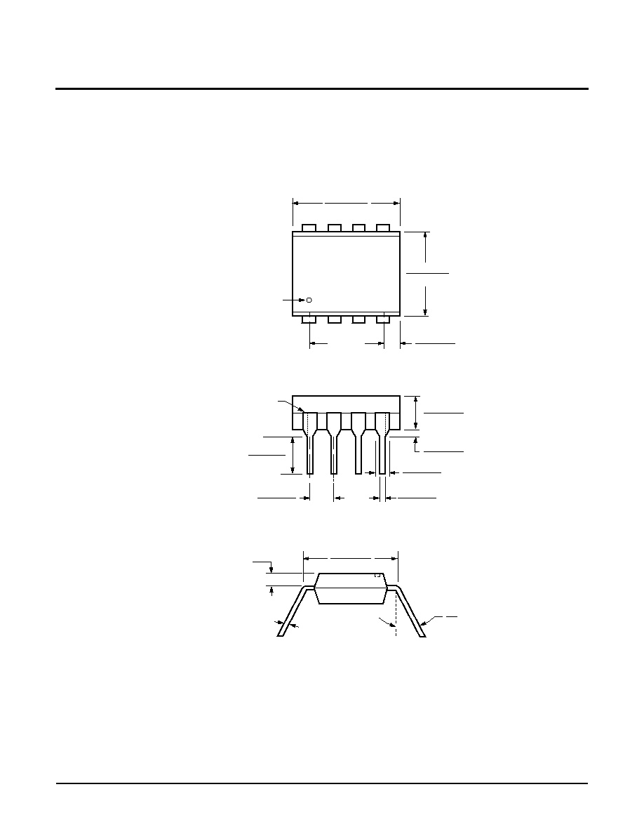
8-LEAD PLASTIC DUAL IN-LINE PACKAGE TYPE P
HALF SHOULDER WIDTH ON
ALL END PINS OPTIONAL
.073 (1.84)
MAX.
0.325 (8.25)
0.300 (7.62)
X76F101
13
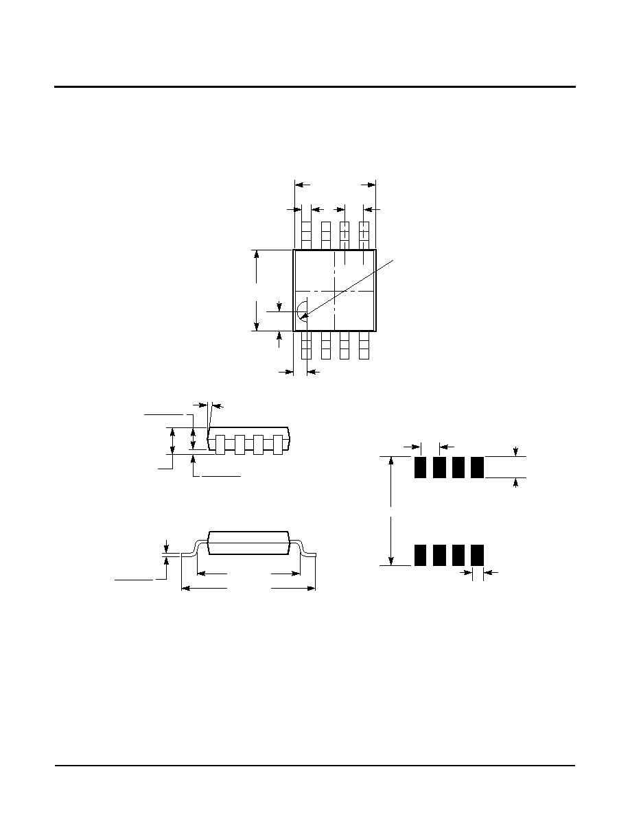
NOTE:
1. ALL DIMENSIONS IN INCHES (IN P
ARENTHESES IN MILLIMETERS)
2. PACKAGE DIMENSIONS EXCLUDE MOLDING FLASH
0.020 (.508)
0.012 (.305)
.080 (2.03)
.070 (1.78)
.213 (5.41)
.205 (5.21)
0
8
.330 (8.38)
.300 (7.62)
.212 (5.38)
.203 (5.16)
.035 (.889)
.020 (.508)
.010 (.254)
.007 (.178)
REF
PIN 1 ID
.050 (1.27) BSC
.013 (.330)
.004 (.102)
7025 FM 24
0.150 (3.80)
0.158 (4.00)
0.228 (5.80)
0.244 (6.20)
0.014 (0.35)
0.019 (0.49)
PIN 1
PIN 1 INDEX
0.010 (0.25)
0.020 (0.50)
0.050 (1.27)
0.188 (4.78)
0.197 (5.00)
0.004 (0.19)
0.010 (0.25)
0.053 (1.35)
0.069 (1.75)
(4X) 7
∞
0.016 (0.410)
0.037 (0.937)
0.0075 (0.19)
0.010 (0.25)
0
∞
≠ 8
∞
X 45
∞
8-LEAD PLASTIC SMALL OUTLINE GULL WING PACKAGE TYPE S
NOTE: ALL DIMENSIONS IN INCHES (IN PARENTHESES IN MILLIMETERS)
0.250"
0.050" TYPICAL
0.050"
TYPICAL
0.030"
TYPICAL
8 PLACES
FOOTPRINT
PACKAGING INFORMATION
X76F101
14
0.118 ± 0.002
(3.00 ± 0.05)
0.040 ± 0.002
(1.02 ± 0.05)
0.150 (3.81)
REF.
0.193 (4.90)
REF.
0.030 (0.76)
0.036 (0.91)
0.032 (0.81)
0.007 (0.18)
0.005 (0.13)
0.008 (0.20)
0.004 (0.10)
0.0216 (0.55)
7∞ TYP
R 0.014 (0.36)
0.118 ± 0.002
(3.00 ± 0.05)
0.012 + 0.006 / -0.002
(0.30 + 0.15 / -0.05)
0.0256 (0.65) TYP
8-LEAD MINIATURE SMALL OUTLINE GULL WING PACKAGE TYPE M
NOTE:
1. ALL DIMENSIONS IN INCHES AND (MILLIMETERS)
3003 ILL 01
0.220"
0.0256" TYPICAL
0.025"
TYPICAL
0.020"
TYPICAL
8 PLACES
FOOTPRINT
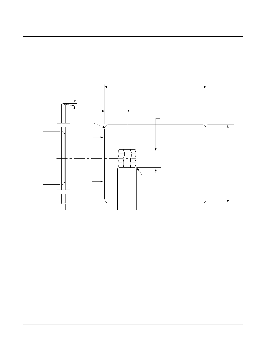
X76F101
15
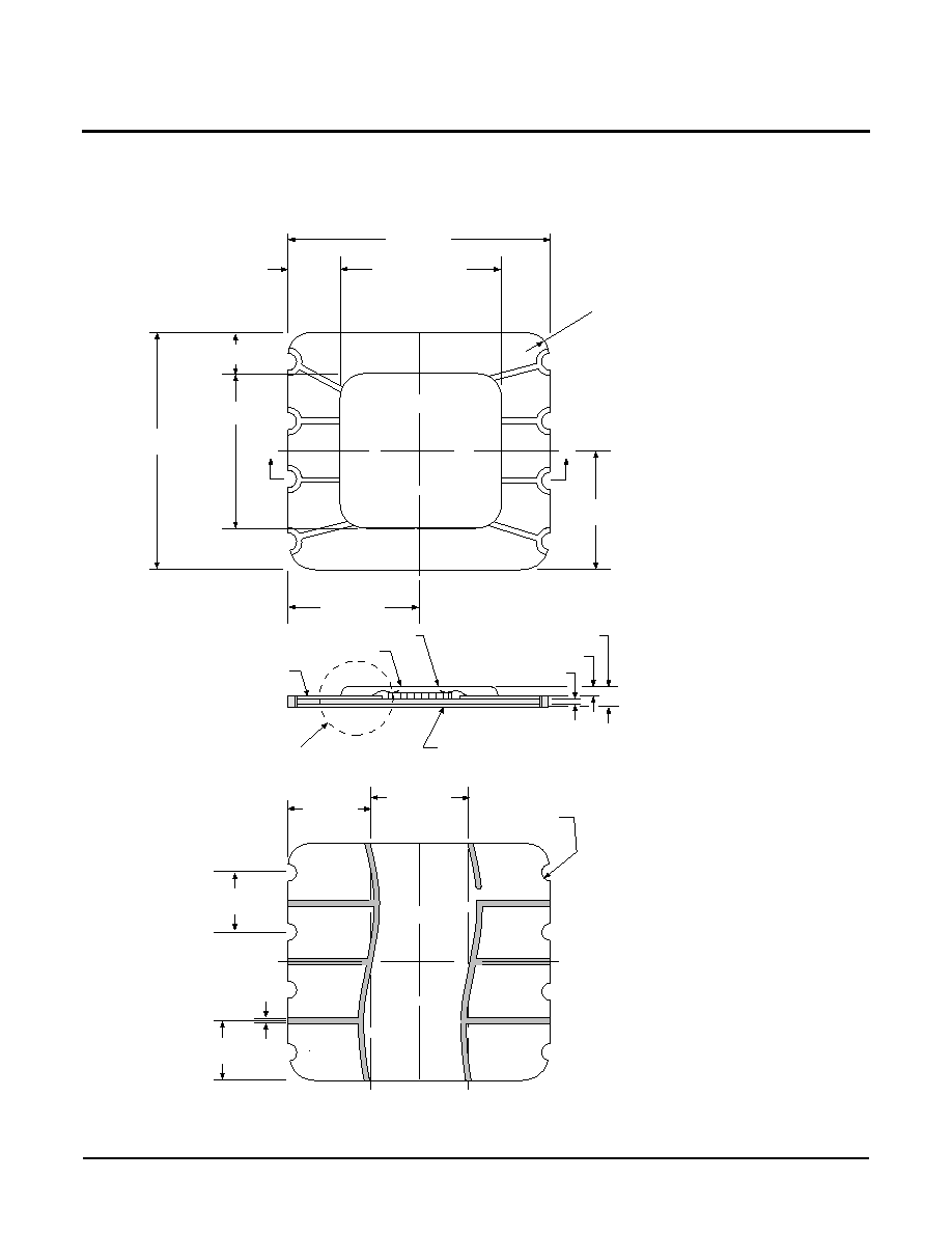
8 PAD CHIP ON BOARD SMART CARD MODULE TYPE X
3.369
±
0.002
(85.57
±
0.05)
2.125
±
0.002
(53.98
±
0.05
0.593
±
0.002
(15.06
±
0.05)
3
∞
MAX.
DRAFT ANGLE
(ALL AROUND)
0.430
±
0.002
(10.92
±
0.05)
0.010
0.25)
R. 0.125
(3.18) (4x)
A
A
R. 0.030 (0.76) (4x)
SMART CARD TYPE Y
X76F101
16
0.465
±
0.002
(11.81
±
0.05)
A
SECTION A-A
A
R. 0.078 (2.00)
0.285 (7.24) MAX.
SEE NOTE 7 SHT. 2
0.420
±
0.002
(10.67
±
0.05)
0.210
±
0.002
(5.33
±
0.05)
0.105
±
0.002
(2.67
±
0.05) TYP.
(8x)
(8x)
0.105
±
0.002
(2.67
±
0.05)
0.008
±
0.001
(0.20
±
0.03)
0.233
±
0.002
(5.92
±
0.05)
0.174
±
0.002
(4.42
±
0.05)
0.146
±
0.002
(3.71
±
0.05)
DIE
0.0235 (0.60) MAX.
0.015 (0.38) MAX.
0.008 (0.20) MAX.
GLOB SIZE
FR4 TAPE
SEE DETAIL SHEET 3
COPPER, NICKEL PLATED, GOLD FLASH
R. 0.013 (0.33) (8x)
0.270 (6.86) MAX.
SEE NOTE 7 SHT. 2
0.069 (1.75) MIN EPOXY
FREE AREA (TYP.)
0.088 (2.24) MIN EPOXY
FREE AREA (TYP.)
X76F041 8 PAD CHIP ON BOARD SMART CARD MODULE TYPE X
NOTE:
1. ALL DIMENSIONS IN INCHES AND (MILLIMETERS)
SC Type X ILL 1.0
Vcc
RST
SCL
NC
Vss
CS
SDA
NC
X76F101
17
ORDERING INFORMATION
V
CC
Limits
Blank = 5V ±10%
3.0 = 3.0V to 5.5V
Temperature Range
Blank = Commercial = 0∞C to +70∞C
I = Industrial= ≠40∞C to +85∞C
Package
S = 8-Lead SOIC
M = 8- Lead MSOP
P = 8-Lead PDIP
H = Die in Waffle Packs
W = Die in Wafer Form
X = Smart Card Module
Y = Smart Card
Device
X76F101
X
X
≠X
Part Mark Convention
8-Lead MSOP
AAQ = 3.0 to 5.5V, 0 to +76∞C
EYWW
XXX
AAR = 3.0 to 5.5V, -40 to +85∞C
AAS = 4.5 to 5.5V, 0 to +76∞C
AAT = 4.5 to 5.5V, -40 to +85∞C
8-Lead SOIC/PDIP
X76F101 X
XX
A = 8-Lead SOIC
D = 3.0 to 5.5V, 0 to +70∞C
E = 3.0 to 5.5V, -40 to +85∞C
Blank = 4.5 to 5.5V, 0 to +70∞C
I = 4.5 to 5.5V, -40 to +85∞C
LIMITED WARRANTY
Devices sold by Xicor, Inc. are covered by the warranty and patent indemnification provisions appearing in its Terms of Sale only. Xicor, Inc. makes no warranty,
express, statutory, implied, or by description regarding the information set forth herein or regarding the freedom of the described devices from patent infringement.
Xicor, Inc. makes no warranty of merchantability or fitness for any purpose. Xicor, Inc. reserves the right to discontinue production and change specifications and
prices at any time and without notice.
Xicor, Inc. assumes no responsibility for the use of any circuitry other than circuitry embodied in a Xicor, Inc. product. No other circuits, patents, licenses are implied.
U.S. PATENTS
Xicor products are covered by one or more of the following U.S. Patents: 4,263,664; 4,274,012; 4,300,212; 4,314,265; 4,326,134; 4,393,481; 4,404,475;
4,450,402; 4,486,769; 4,488,060; 4,520,461; 4,533,846; 4,599,706; 4,617,652; 4,668,932; 4,752,912; 4,829, 482; 4,874, 967; 4,883, 976. Foreign patents and
additional patents pending.
LIFE RELATED POLICY
In situations where semiconductor component failure may endanger life, system designers using this product should design the system with appropriate error
detection and correction, redundancy and back-up features to prevent such an occurence.
Xicor's products are not authorized for use in critical components in life support devices or systems.
1. Life support devices or systems are devices or systems which, (a) are intended for surgical implant into the body, or (b) support or sustain life, and whose failure
to perform, when properly used in accordance with instructions for use provided in the labeling, can be reasonably expected to result in a significant injury to the
user.
2. A critical component is any component of a life support device or system whose failure to perform can be reasonably expected to cause the failure of the life
support device or system, or to affect its safety or effectiveness.