Document Outline
- Table of Contents
- Product Selection
- Data Sheet Alpha
- Ap Note Alpha

©
Xicor, Inc. 1994, 1997Patents Pending
7008-1.2 8/26/97 T2/C0/D0 SH
1
Characteristics subject to change without notice
A
PPLICATION
N
OTE
A V A I L A B L E
16K/64K/128K
MPS
TM
EEPROM
µ
Port Saver EEPROM
FEATURES
∑ Up to 10MHz data transfer rate
∑ 25ns Read Access Time
∑ Direct Interface to Microprocessors and
Microcontrollers
--Eliminates I/O port requirements
--No interface glue logic required
--Eliminates need for parallel to serial converters
∑ Low Power CMOS
--1.8V≠3.6V, 2.5V≠5.5V and 5V
±
10% Versions
--Standby Current Less than 1
µ
A
--Active Current Less than 1mA
∑ Byte or Page Write Capable
--32-Byte Page Write Mode
∑ Typical Nonvolatile Write Cycle Time: 2ms
∑ High Reliability
--100,000 Endurance Cycles
--Guaranteed Data Retention: 100 Years
DESCRIPTION
The
µ
Port Saver memories need no serial ports or spe-
cial hardware and connect to the processor memory bus.
Replacing bytewide data memory, the
µ
Port Saver uses
bytewide memory control functions, takes a fraction of
the board space and consumes much less power.
Replacing serial memories, the
µ
Port Saver provides all
the serial benefits, such as low cost, low power, low volt-
age, and small package size while releasing I/Os for
more important uses.
The
µ
Port Saver memory outputs data within 25ns of an
active read signal. This is less than the read access time
of most hosts and provides "no-wait-state" operation.
This prevents bottlenecks on the bus. With rates to 10
MHz, the
µ
Port Saver supplies data faster than required
by most host read cycle specifications. This eliminates
the need for software NOPs.
The
µ
Port Saver memories communicate over one line of
the data bus using a sequence of standard bus read and
write operations. This "bit serial" interface allows the
µ
Port Saver to work well in 8-bit, 16 bit, 32-bit, and 64-bit
systems.
A Write Protect (WP) pin prevents inadvertent writes to
the memory.
Xicor EEPROMs are designed and tested for applica-
tions requiring extended endurance. Inherent data reten-
tion is greater than 100 years.
BLOCK DIAGRAM
CE
I/O
H.V. GENERATION
TIMING & CONTROL
EEPROM
COMMAND
DECODE
AND
CONTROL
LOGIC
X
DEC
Y DECODE
DATA REGISTER
WP
7008 FRM F02.1
OE
WE
ARRAY
16K x 8
P0/CS
P1/CLK
P2/DI
P3/DO
System Connection
Internal Block Diagram
µ
P
µ
C
Ports
8K x 8
2K x 8
Saved
DSP
ASIC
A15
A0
D7
D0
OE
WE
MPS
RISC
X84161/641/129
AN95 ∑ AN103 ∑ AN107
X84161/641/129
2
PIN DESCRIPTIONS
Chip Enable (CE)
The Chip Enable input must be LOW to enable all read/
write operations. When CE is HIGH, the chip is dese-
lected, the I/O pin is in the high impedance state, and
unless a nonvolatile write operation is underway, the
device is in the standby power mode.
Output Enable (OE)
The Output Enable input must be LOW to enable the out-
put buffer and to read data from the device on the I/O line.
Write Enable (WE)
The Write Enable input must be LOW to write either data
or command sequences to the device.
Data In/Data Out (I/O)
Data and command sequences are serially written to or
serially read from the device through the I/O pin.
Write Protect (WP)
When the Write Protect input is LOW, nonvolatile writes
to the device are disabled. When WP is HIGH, all func-
tions, including nonvolatile writes, operate normally. If a
nonvolatile write cycle is in progress, WP going LOW will
have no effect on the cycle already underway, but will
inhibit any additional nonvolatile write cycles.
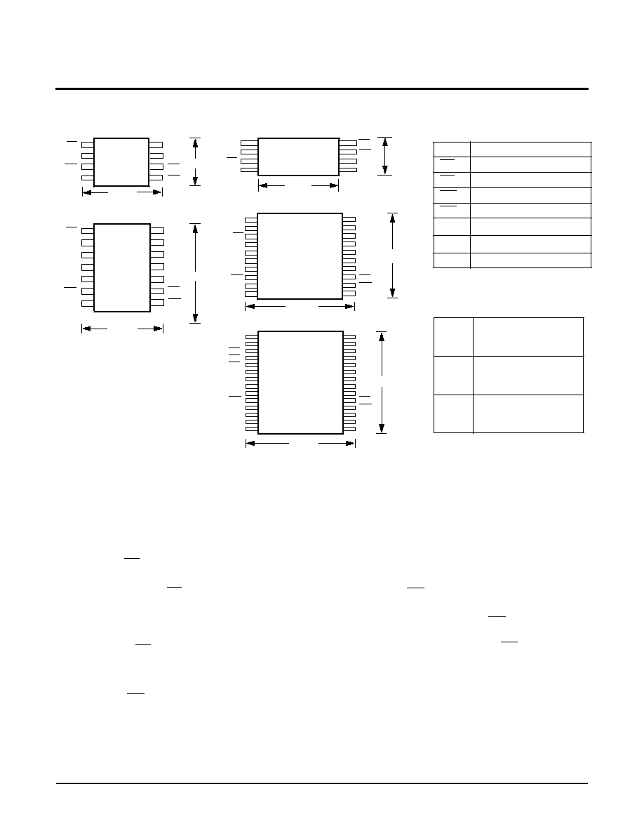
PIN CONFIGURATIONS:
Drawings are to the same scale, actual package sizes are shown in inches:
VCC
NC
OE
WE
CE
I/O
WP
VSS
1
2
3
4
8
7
6
5
8-LEAD SOIC
7008 FRM F01
1
2
3
4
5
6
7
8
14
13
12
11
10
9
14-LEAD SOIC
CE
I/O
NC
NC
NC
WP
VSS
V CC
NC
NC
NC
NC
OE
WE
PIN NAMES
7008 FRM T01
I/O
Data Input/Output
CE
Chip Enable Input
OE
Output Enable Input
WE
Write Enable Input
WP
Write Protect Input
V
CC
Supply Voltage
V
SS
Ground
NC
No Connect
PACKAGE
SELECTION GUIDE
7008 FRM T0A
84161
8-Lead PDIP
8-Lead SOIC
8-Lead TSSOP
84641
8-Lead PDIP
8-Lead SOIC
20-Lead TSSOP
84129
8-Lead PDIP
14-Lead SOIC
28-Lead TSSOP
1
2
3
4
5
6
7
20
19
18
17
16
15
14
20-LEAD TSSOP
CE
I/O
NC
NC
NC
WP
VSS
VCC
NC
NC
NC
NC
OE
WE
8
9
10
13
12
11
NC
NC
NC
NC
NC
NC
1
2
3
4
5
6
7
20
19
18
17
16
15
28-LEAD TSSOP
NC
NC
WP
V
SS
NC
NC
NC
OE
WE
NC
NC
8
9
10
I/O
CE
NC
V
CC
NC
NC
CE
CE
NC
NC
NC
NC
NC
NC
11
12
13
14
21
22
23
24
25
26
27
28
X84161
X84641
X84129
.190 in.
.230 in.
.230 in.
.390 in.
.250 in.
.394 in.
.252 in.
. 252 in.
X84129
X84641
NC
NC
NC
OE
NC
V
CC
CE
I/O
1
2
3
4
8
7
6
5
8-LEAD TSSOP
X84161
.114 in.
.252 in.
WE
WP
VSS
8-LEAD PDIP
X84161/641/129
3
DEVICE OPERATION
The X84161/641/129 are serial EEPROMs designed to
interface directly with most microprocessor buses. Stan-
dard CE, OE, and WE signals control the read and write
operations, and a single l/O line is used to send and
receive data and commands serially.
Data Timing
Data input on the l/O line is latched on the rising edge of
either WE or CE, whichever occurs first. Data output on
the l/O line is active whenever both OE and CE are LOW.
Care should be taken to ensure that WE and OE are
never both LOW while CE is LOW.
Read Sequence
A read sequence consists of sending a 16-bit address
followed by the reading of data serially. The address is
written by issuing 16 separate write cycles (WE and CE
LOW, OE HIGH) to the part without a read cycle between
the write cycles. The address is sent serially, most signifi-
cant bit first, over the I/O line. Note that this sequence is
fully static, with no special timing restrictions, and the pro-
cessor is free to perform other tasks on the bus when-
ever the device CE pin is HIGH. Once the 16 address
bits are sent, a byte of data can be read on the I/O line by
issuing 8 separate read cycles (OE and CE LOW, WE
HIGH). At this point, writing a `1' will terminate the read
sequence and enter the low power standby state, other-
wise the device will await further reads in the sequential
read mode.
Sequential Read
The byte address is automatically incremented to the
next higher address after each byte of data is read. The
data stored in the memory at the next address can be
read sequentially by continuing to issue read cycles.
When the highest address in the array is reached, the
address counter rolls over to address $0000 and reading
may be continued indefinitely.
Reset Sequence
The reset sequence resets the device and sets an inter-
nal write enable latch. A reset sequence can be sent at
any time by performing a read/write "0"/read operation
(see Figs. 1 and 2). This breaks the multiple read or write
cycle sequences that are normally used to read from or
write to the part. The reset sequence can be used at any
time to interrupt or end a sequential read or page load.
As soon as the write "0" cycle is complete, the part is
reset (unless a nonvolatile write cycle is in progress). The
second read cycle in this sequence, and any further read
cycles, will read a HIGH on the l/O pin until a valid read
sequence (which includes the address) is issued. The
reset sequence must be issued at the beginning of both
read and write sequences to be sure the device initiates
these operations properly.
Figure 1. Read Sequence
CE
OE
WE
I/O (IN)
"0"
RESET
WHEN ACCESSING:
X84161 ARRAY: A15≠A11=0
X84641 ARRAY: A15≠A13=0
X84129 ARRAY: A15≠A14=0
LOAD ADDRESS
READ DATA
A15 A14 A13 A12 A11 A10 A9 A8
A7 A6
A5 A4
A3 A2
A1 A0
I/O (OUT)
7008 FRM F04.1
D7 D6 D5 D4 D3 D2 D1 D0
X84161/641/129
4
Write Sequence
A nonvolatile write sequence consists of sending a reset
sequence, a 16-bit address, up to 32 bytes of data, and
then a special "start nonvolatile write cycle" command
sequence.
The reset sequence is issued first (as described in the
Reset Sequence section) to set an internal write enable
latch. The address is written serially by issuing 16
separate write cycles (WE and CE LOW, OE HIGH) to
the part without any read cycles between the writes. The
address is sent serially, most significant bit first, on the
l/O pin. Up to 32 bytes of data are written by issuing a
multiple of 8 write cycles. Again, no read cycles are
allowed between writes.
The nonvolatile write cycle is initiated by issuing a special
read/write "1"/read sequence. The first read cycle ends
the page load, then the write "1" followed by a read starts
the nonvolatile write cycle. The device recognizes 32-
byte pages (e.g., beginning at addresses XXXXXX00000
for X84161).
When sending data to the part, attempts to exceed the
upper address of the page will result in the address
counter "wrapping-around" to the first address on the
page, where data loading can continue. For this reason,
sending more than 256 consecutive data bits will result in
overwriting previous data.
A nonvolatile write cycle will not start if a partial or incom-
plete write sequence is issued. The internal write enable
latch is reset when the nonvolatile write cycle is com-
pleted and after an invalid write to prevent inadvertent
writes. Note that this sequence is fully static, with no spe-
cial timing restrictions. The processor is free to perform
other tasks on the bus whenever the chip enable pin (CE)
is HIGH.
Nonvolatile Write Status
The status of a nonvolatile write cycle can be determined
at any time by simply reading the state of the l/O pin on
the device. This pin is read when OE and CE are LOW
and WE is HIGH. During a nonvolatile write cycle the l/O
pin is LOW. When the nonvolatile write cycle is complete,
the l/O pin goes HIGH. A reset sequence can also be
issued during a nonvolatile write cycle with the same
result: I/O is LOW as long as a nonvolatile write cycle is
in progress, and l/O is HIGH when the nonvolatile write
cycle is done.
Figure 2: Write Sequence
CE
OE
WE
I/O (IN)
"0"
"0"
"1"
RESET
LOAD ADDRESS
LOAD DATA
START
NONVOLATILE
WRITE
A8
A7
A6 A5 A4 A3 A2
A1 A0
D7 D6 D5 D4 D3 D2 D1 D0
I/O (OUT)
7008 FRM F05.1
WHEN ACCESSING:
X84161 ARRAY: A15≠A11=0
X84641 ARRAY: A15≠A13=0
X84129 ARRAY: A15≠A14=0
A15 A14 A13 A12 A11 A10 A9
X84161/641/129
5
Low Power Operation
The device enters an idle state, which draws minimal cur-
rent when:
--an illegal sequence is entered. The following are the
more common illegal sequences:
∑ Read/Write/Write--any time
∑ Read/Write `1'--When writing the address or
writing data.
∑ Write `1'--when reading data
∑ Read/Read/Write `1'--after data is written to
device, but before entering the NV write sequence.
--the device powers-up;
--a nonvolatile write operation completes.
While a sequential read is in progress, the device
remains in an active state. This state draws more current
than the idle state, but not as much as during a read
itself. To go back to the lowest power condition, an invalid
condition is created by writing a `1' after the last bit of a
read operation.
Write Protection
The following circuitry has been included to prevent
inadvertent nonvolatile writes:
--The internal Write Enable latch is reset upon
power-up.
--A reset sequence must be issued to set the internal
write enable latch before starting a write sequence.
--A special "start nonvolatile write" command sequence
is required to start a nonvolatile write cycle.
--The internal Write Enable latch is reset automatically
at the end of a nonvolatile write cycle.
--The internal Write Enable latch is reset and remains
reset as long as the WP pin is LOW, which blocks all
nonvolatile write cycles.
--The internal Write Enable latch resets on an invalid
write operation.
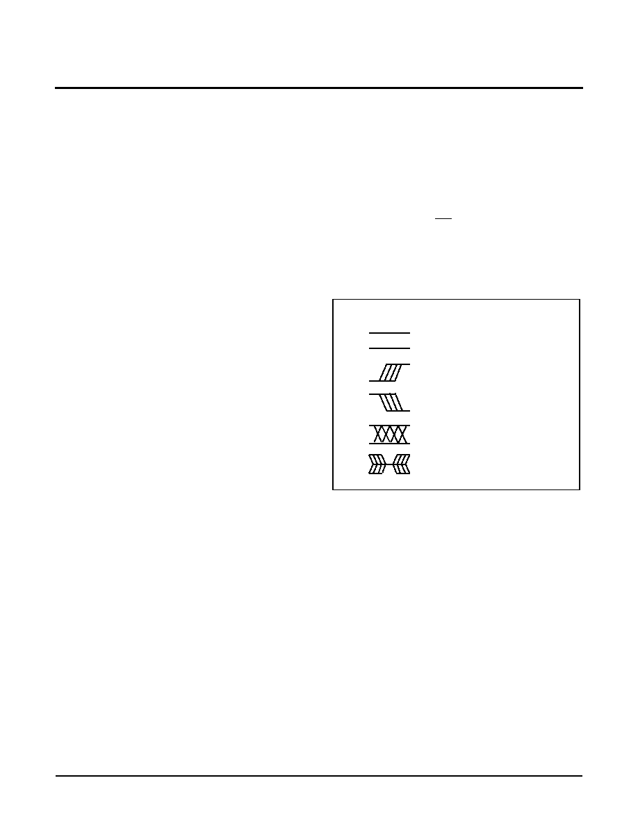
SYMBOL TABLE
WAVEFORM
INPUTS
OUTPUTS
Must be
steady
Will be
steady
May change
from LOW to
HIGH
Will change
from LOW to
HIGH
May change
from HIGH to
LOW
Will change
from HIGH to
LOW
Don't Care:
Changes
Allowed
Changing:
State Not
Known
N/A
Center Line
is High
Impedance

X84161/641/129
6
ABSOLUTE MAXIMUM RATINGS*
Temperature under Bias ...................... ≠65
∞
C to +135
∞
C
Storage Temperature ........................... ≠65
∞
C to +150
∞
C
Terminal Voltage with
Respect to V
SS
.......................................≠1V to +7V
DC Output Current................................................... 5mA
Lead Temperature (Soldering, 10 seconds)..........300
∞
C
RECOMMENDED OPERATING CONDITIONS
7008 FRM T02
*COMMENT
Stresses above those listed under "Absolute Maximum
Ratings" may cause permanent damage to the device.
This is a stress rating only and the functional operation
of the device at these or any other conditions above
those indicated in the operational sections of this speci-
fication is not implied. Exposure to absolute maximum
rating conditions for extended periods may affect device
reliability.
7008 FRM T03
Temperature
Min.
Max.
Commercial
0
∞
C
+70
∞
C
Industrial
≠40
∞
C
+85
∞
C
Military
≠55
∞
C
+125
∞
C
Supply Voltage
Limits
X84161/641/129
5V
±
10%
X84161/641/129 ≠ 2.5
2.5V to 5.5V
X84161/641/129 ≠ 1.8
1.8V to 3.6V
D.C. OPERATING CHARACTERISTICS (V
CC
= 5V
±
10%)
(Over the recommended operating conditions, unless otherwise specified.)
7008 FRM T04.2
Notes:
(1) V
IL
Min. and V
IH
Max. are for reference only and are not tested.
Symbol
Parameter
Limits
Units
Test Conditions
Min.
Max.
I
CC1
V
CC
Supply Current (Read)
1
mA
OE = V
IL
, WE = V
IH
,
I/O = Open, CE clocking @ 10MHz
I
CC2
V
CC
Supply Current (Write)
2
mA
I
CC
During Nonvolatile Write Cycle
All Inputs at CMOS Levels
I
SB1
V
CC
Standby Current
1
µ
A
CE = V
CC
, Other Inputs = V
CC
or V
SS
I
LI
Input Leakage Current
10
µ
A
V
IN
= V
SS
to V
CC
I
LO
Output Leakage Current
10
µ
A
V
OUT
= V
SS
to V
CC
V
lL
(1)
Input LOW Voltage
≠0.5
V
CC
x 0.3
V
V
IH
(1)
Input HIGH Voltage
V
CC
x 0.7
V
CC
+ 0.5
V
V
OL
Output LOW Voltage
0.4
V
I
OL
= 2.1mA
V
OH
Output HIGH Voltage
V
CC
≠ 0.8
V
I
OH
= ≠1mA
Notes:
Contact factory for Military availability

X84161/641/129
7
D.C. OPERATING CHARACTERISTICS (V
CC
= 2.5V to 5.5V)
(Over the recommended operating conditions, unless otherwise specified.)
7008 FRM T05.1
D.C. OPERATING CHARACTERISTICS (V
CC
= 1.8V to 3.6V)
(Over the recommended operating conditions, unless otherwise specified.)
7008 FRM T05.1
Notes: (1) V
IL
Min. and V
IH
Max. are for reference only and are not tested.
Symbol
Parameter
Limits
Units
Test Conditions
Min.
Max.
I
CC1
V
CC
Supply Current (Read)
500
µ
A
OE = V
IL
, WE = V
IH
,
I/O = Open, CE clocking @ 5MHz
I
CC2
V
CC
Supply Current (Write)
2
mA
I
CC
During Nonvolatile Write Cycle
All Inputs at CMOS Levels
I
SB1
V
CC
Standby Current
1
µ
A
CE = V
CC
, Other Inputs = V
CC
or V
SS
I
LI
Input Leakage Current
10
µ
A
V
IN
= V
SS
to V
CC
I
LO
Output Leakage Current
10
µ
A
V
OUT
= V
SS
to V
CC
V
lL
(1)
Input LOW Voltage
≠0.5
V
CC
x 0.3
V
V
IH
(1)
Input HIGH Voltage
V
CC
x 0.7
V
CC
+ 0.5
V
V
OL
Output LOW Voltage
0.4
V
I
OL
= 1mA, V
CC
= 3V
V
OH
Output HIGH Voltage
V
CC
≠ 0.4
V
I
OH
= ≠400
µ
A, V
CC
= 3V
Symbol
Parameter
Limits
Units
Test Conditions
Min.
Max.
I
CC1
V
CC
Supply Current (Read)
300
µ
A
OE = V
IL
, WE = V
IH
,
I/O = Open, CE clocking @ 3MHz
I
CC2
V
CC
Supply Current (Write)
1
mA
I
CC
During Nonvolatile Write Cycle
All Inputs at CMOS Levels
I
SB1
V
CC
Standby Current
1
µ
A
CE = V
CC
, Other Inputs = V
CC
or V
SS
I
LI
Input Leakage Current
10
µ
A
V
IN
= V
SS
to V
CC
I
LO
Output Leakage Current
10
µ
A
V
OUT
= V
SS
to V
CC
V
lL
(1)
Input LOW Voltage
≠0.5
V
CC
x 0.3
V
V
IH
(1)
Input HIGH Voltage
V
CC
x 0.7
V
CC
+ 0.5
V
V
OL
Output LOW Voltage
0.4
V
I
OL
= 0.5mA, V
CC
= 2V
V
OH
Output HIGH Voltage
V
CC
≠ 0.2
V
I
OH
= ≠250
µ
A, V
CC
= 2V
X84161/641/129
8
CAPACITANCE
T
A
= +25
∞
C, f = 1MHz, V
CC
= 5V
7008 FRM T06
Notes: (2) Periodically sampled, but not 100% tested.
POWER-UP TIMING
7008 FRM T07
Notes: (3) Time delays required from the time the V
CC
is stable until the specific operation can be initiated.
Periodically sampled, but not 100% tested.
A.C. CONDITIONS OF TEST
7008 FRM T08
EQUIVALENT A.C. LOAD CIRCUITS
Symbol
Parameter
Max.
Units
Test Conditions
C
I/O
(2)
Input/Output Capacitance
8
pF
V
I/O
= 0V
C
IN
(2)
Input Capacitance
6
pF
V
IN
= 0V
Symbol
Parameter
Max.
Units
t
PUR
(3)
Power-up to Read Operation
2
ms
t
PUW
(3)
Power-up to Write Operation
5
ms
Input Pulse Levels
V
CC
x 0.1 to V
CC
x 0.9
Input Rise and Fall Times
5ns
Input and Output Timing Levels
V
CC
x 0.5
5V
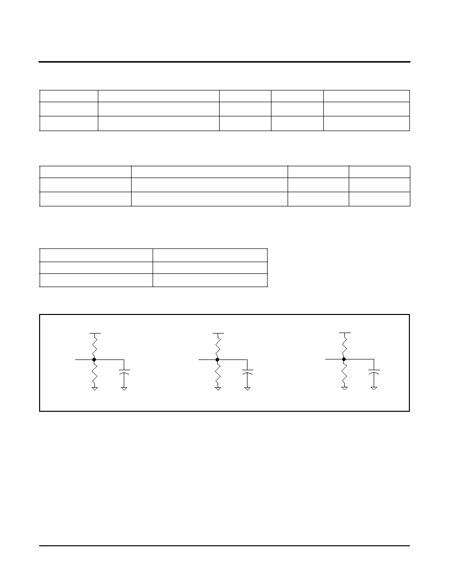
30pF
2.06K
3.03K
OUTPUT
7008 FRM F06
3V
30pF
2.39K
4.58K
OUTPUT
7008 FRM F07
2V
30pF
2.8K
5.6K
OUTPUT
X84161/641/129
9
A.C. CHARACTERISTICS
(Over the recommended operating conditions, unless otherwise specified.)
Read Cycle Limits ≠ X84161/641/129
Notes: (4) Periodically sampled, but not 100% tested. t
HZ
and t
OHZ
are measured from the point where CE or OE goes HIGH (whichever occurs
first) to the time when I/O is no longer being driven into a 5pF load.
Contact factory for 10MHz X84129 availabilityRead Cycle
Symbol
Parameter
V
CC
= 5V
±
10%
V
CC
= 2.5V ≠ 5.5V V
CC
= 1.8V ≠ 3.6V
Units
Min.
Max
Min.
Max.
Min.
Max.
t
RC
Read Cycle Time
100
200
330
ns
t
CE
CE Access Time
25
50
70
ns
t
OE
OE Access Time
25
50
70
ns
t
OEL
OE Pulse Width
50
60
90
ns
t
OEH
OE High Recovery Time
50
60
90
ns
t
LOW
CE LOW Time
50
70
90
ns
t
HIGH
CE HIGH Time
50
120
180
ns
t
LZ
(4)
CE LOW to Output In Low Z
0
0
0
ns
t
HZ
(4)
CE HIGH to Output In High Z
0
25
0
30
0
35
ns
t
OLZ
(4)
OE LOW to Output In Low Z
0
0
0
ns
t
OHZ
(4)
OE HIGH to Output In High Z
0
25
0
30
0
35
ns
t
OH
Output Hold from CE or OE HIGH
0
0
0
ns
t
WES
WE HIGH Setup Time
25
25
25
ns
t
WEH
WE HIGH Hold Time
25
25
25
ns
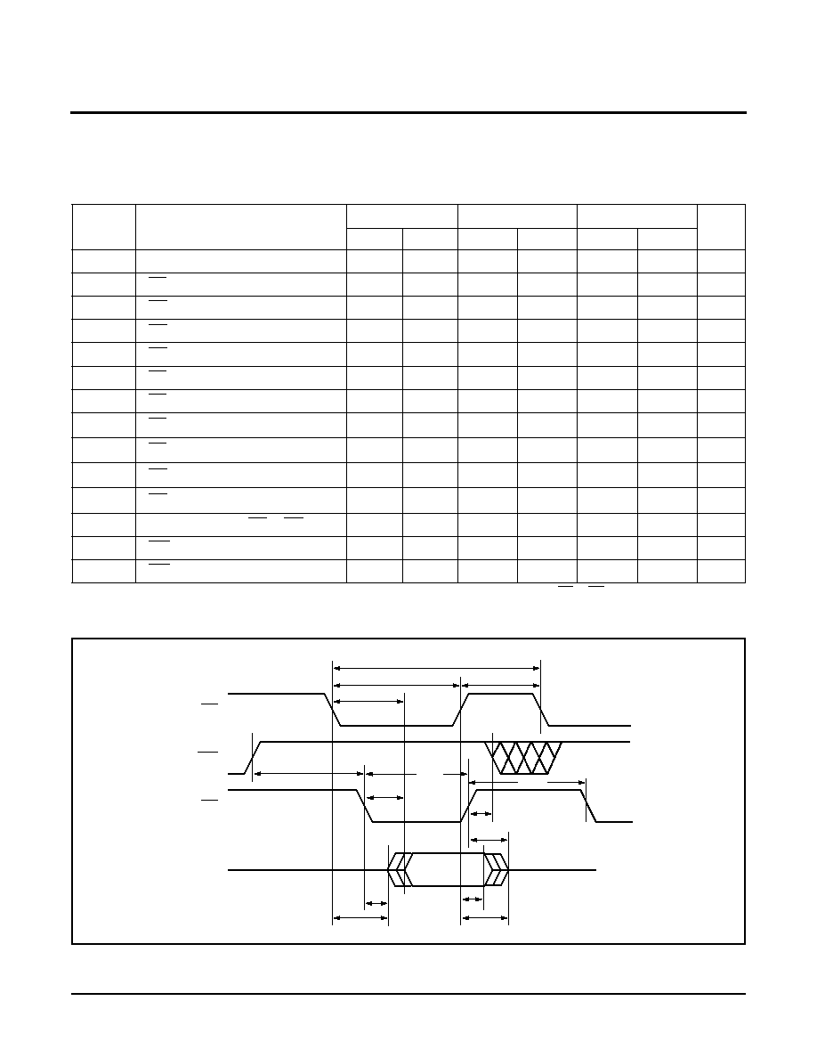
CE
WE
tWES
OE
7008 FRM F08
tHIGH
tCE
tOE
t OLZ
tOH
tWEH
HIGH Z
DATA
t OHZ
t HZ
t LZ
tLOW
tRC
I/O
OEL
t
tOEH

X84161/641/129
10
Write Cycle Limits ≠ X84161/641/129
7008 FRM T10
Notes: (5) t
NVWC
is the time from the falling edge of OE or CE (whichever occurs last) of the second read cycle in the "start nonvolatile write cycle"
sequence until the self-timed, internal nonvolatile write cycle is completed.
(6) Data is latched into the X84161/641/129 on the rising edge of CE or WE, whichever occurs first.
(7) Periodically sampled, but not 100% tested.
Symbol
Parameter
V
CC
= 5V
±
10%
V
CC
= 2.5V ≠ 5.5V V
CC
= 1.8V ≠ 3.6V
Units
Min.
Max.
Min.
Max.
Min.
Max.
t
NVWC
(5)
Nonvolatile Write Cycle Time
5
5
5
ms
t
WC
Write Cycle Time
100
200
330
ns
t
WP
WE Pulse Width
25
40
70
ns
t
WPH
WE HIGH Recovery Time
65
150
200
ns
t
CS
Write Setup Time
0
0
0
ns
t
CH
Write Hold Time
0
0
0
ns
t
CP
CE Pulse Width
25
40
70
ns
t
CPH
CE HIGH Recovery Time
65
150
200
ns
t
OES
OE HIGH Setup Time
25
25
50
ns
t
OEH
OE HIGH Hold Time
25
25
50
ns
t
DS
(6)
Data Setup Time
12
20
30
ns
t
DH
(6)
Data Hold Time
5
5
5
ns
t
WPSU
(7)
WP HIGH Setup
100
100
150
ns
t
WPHD
(7)
WP HIGH Hold
100
100
150
ns
X84161/641/129
11
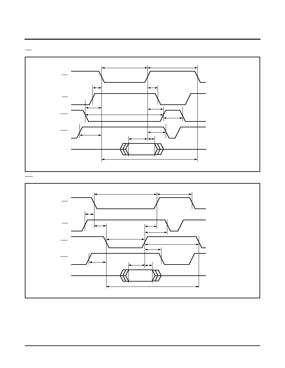
CE Controlled Write Cycle
WE Controlled Write Cycle
CE
OE
tWPH
WE
7008 FRM F09
WP
I/O
tOES
tCPH
tOEH
tCH
tWPHD
HIGH Z
DATA
tDS
tDH
tCP
tWP
tWPSU
tCS
tWC
CE
OE
tWPH
WE
7008 FRM F10
WP
I/O
tOES
tCPH
tCH
tOEH
t WPHD
HIGH Z
DATA
tDS
t DH
tCP
tWP
tWPSU
t CS
tWC
X84161/641/129
12
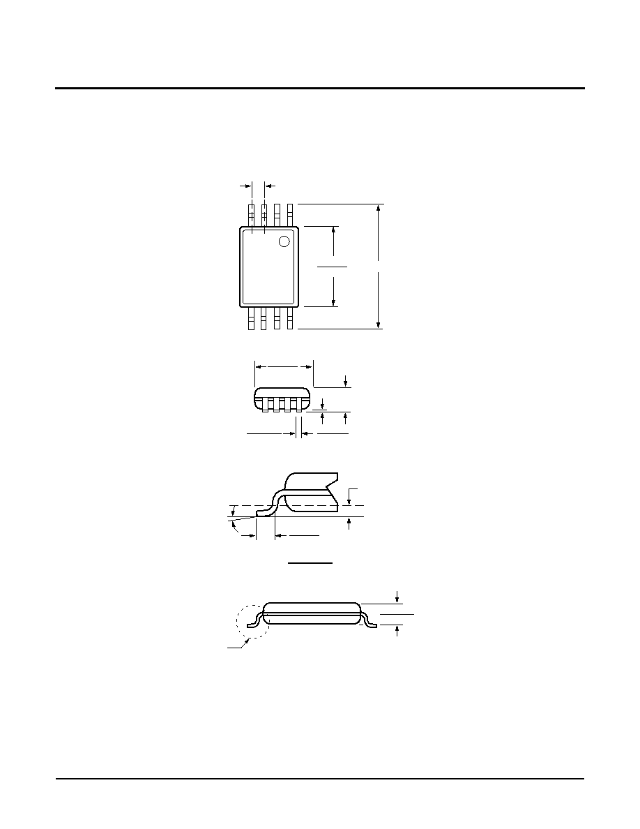
NOTE:
1. ALL DIMENSIONS IN INCHES (IN PARENTHESES IN MILLIMETERS)
2. PACKAGE DIMENSIONS EXCLUDE MOLDING FLASH
0.020 (0.51)
0.016 (0.41)
0.150 (3.81)
0.125 (3.18)
0.110 (2.79)
0.090 (2.29)
0.430 (10.92)
0.360 (9.14)
0.300
(7.62) REF.
PIN 1 INDEX
0.145 (3.68)
0.128 (3.25)
0.025 (0.64)
0.015 (0.38)
PIN 1
SEATING
PLANE
0.065 (1.65)
0.045 (1.14)
0.260 (6.60)
0.240 (6.10)
0.060 (1.52)
0.020 (0.51)
TYP .0.010 (0.25)
0
∞
15
∞
8-LEAD PLASTIC DUAL IN-LINE PACKAGE TYPE P
HALF SHOULDER WIDTH ON
ALL END PINS OPTIONAL
.073 (1.84)
MAX.
0.325 (8.25)
0.300 (7.62)

X84161/641/129
13
0.150 (3.80)
0.158 (4.00)
0.228 (5.80)
0.244 (6.20)
0.014 (0.35)
0.019 (0.49)
PIN 1
PIN 1 INDEX
0.010 (0.25)
0.020 (0.50)
0.050 (1.27)
0.188 (4.78)
0.197 (5.00)
0.004 (0.19)
0.010 (0.25)
0.053 (1.35)
0.069 (1.75)
(4X) 7
∞
0.016 (0.410)
0.037 (0.937)
0.0075 (0.19)
0.010 (0.25)
0
∞
≠ 8
∞
X 45
∞
3926 FRM F22.1
8-LEAD PLASTIC SMALL OUTLINE GULL WING PACKAGE TYPE S
0.250"
0.050" TYPICAL
0.050"
TYPICAL
0.030"
TYPICAL
8 PLACES
FOOTPRINT
NOTE: ALL DIMENSIONS IN INCHES (IN PARENTHESES IN MILLIMETERS)

X84161/641/129
14
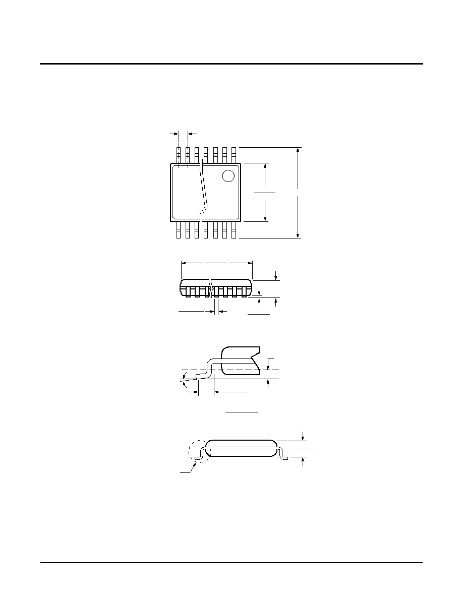
PACKAGING INFORMATION
3926 FRM F26
0.150 (3.80)
0.158 (4.00)
0.228 (5.80)
0.244 (6.20)
0.014 (0.35)
0.020 (0.51)
PIN 1
PIN 1 INDEX
0.050 (1.27)
0.336 (8.55)
0.345 (8.75)
0.004 (0.10)
0.010 (0.25)
0.053 (1.35)
0.069 (1.75)
(4X) 7
∞
14-LEAD PLASTIC SMALL OUTLINE GULL WING PACKAGE TYPE S
NOTE: ALL DIMENSIONS IN INCHES (IN PARENTHESES IN MILLIMETERS)
0.250"
0.050"
T
ypical
0.050"
T
ypical
0.030"
T
ypical
14 Places
FOO
TPRINT
0.010 (0.25)
0.020 (0.50)
0.016 (0.410)
0.037 (0.937)
0.0075 (0.19)
0.010 (0.25)
0
∞
≠ 8
∞
X 45
∞
X84161/641/129
15
PACKAGING INFORMATION
NOTE:
ALL DIMENSIONS IN INCHES (IN PARENTHESES IN MILLIMETERS)
8-LEAD PLASTIC, TSSOP, PACKAGE TYPE V
See Detail "A"
.031 (.80)
.041 (1.05)
.169 (4.3)
.177 (4.5)
.252 (6.4) BSC
.025 (.65) BSC
.114 (2.9)
.122 (3.1)
.002 (.05)
.006 (.15)
.047 (1.20)
.0075 (.19)
.0118 (.30)
0
∞
≠ 8
∞
.010 (.25)
.019 (.50)
.029 (.75)
Gage Plane
Seating Plane
Detail A (20X)
X84161/641/129
16
PACKAGING INFORMATION
NOTE:
ALL DIMENSIONS IN INCHES (IN PARENTHESES IN MILLIMETERS)
20-LEAD PLASTIC, TSSOP P ACKAGE TYPE V
.169 (4.3)
.177 (4.5)
.252 (6.4) BSC
.025 (.65) BSC
.252 (6.4)
.300 (6.6)
.002 (.05)
.006 (.15)
.047 (1.20)
.0075 (.19)
.0118 (.30)
3926 FRM F45
See Detail "A"
.031 (.80)
.041 (1.05)
0
∞
≠ 8
∞
.010 (.25)
.019 (.50)
.029 (.75)
Gage Plane
Seating Plane
Detail A (20X)

X84161/641/129
17
PACKAGING INFORMATION
NOTE:
ALL DIMENSIONS IN INCHES (IN PARENTHESES IN MILLIMETERS)
28-LEAD PLASTIC, TSSOP P ACKAGE TYPE V
.169 (4.3)
.177 (4.5)
.252 (6.4) BSC
.025 (.65) BSC
.394 (10.0)
.002 (.05)
.006 (.15)
.047 (1.20)
.0075 (.19)
.0118 (.30)
3926 FRM F45
See Detail "A"
.031 (.80)
.041 (1.05)
0
∞
≠ 8
∞
.010 (.25)
.019 (.50)
.029 (.75)
Gage Plane
Seating Plane
Detail A (20X)
X84161/641/129
18
ORDERING INFORMATION
*PART MARK CONVENTION
Device
X84161/641/129
X
X
Temperature Range
Blank = Commercial = 0
∞
C to +70
∞
C
I = Industrial = ≠40
∞
C to +85
∞
C
LIMITED WARRANTY
Devices sold by Xicor, Inc. are covered by the warranty and patent indemnification provisions appearing in its Terms of Sale only. Xicor, Inc.
makes no warranty, express, statutory, implied, or by description regarding the information set forth herein or regarding the freedom of the
described devices from patent infringement. Xicor, Inc. makes no warranty of merchantability or fitness for any purpose. Xicor, Inc. reserves the
right to discontinue production and change specifications and prices at any time and without notice.
Xicor, Inc. assumes no responsibility for the use of any circuitry other than circuitry embodied in a Xicor, Inc. product. No other circuits, patents,
licenses are implied.
U.S. PATENTS
Xicor products are covered by one or more of the following U.S. Patents: 4,263,664; 4,274,012; 4,300,212; 4,314,265; 4,326,134; 4,393,481;
4,404,475; 4,450,402; 4,486,769; 4,488,060; 4,520,461; 4,533,846; 4,599,706; 4,617,652; 4,668,932; 4,752,912; 4,829, 482; 4,874, 967;
4,883, 976. Foreign patents and additional patents pending.
LIFE RELATED POLICY
In situations where semiconductor component failure may endanger life, system designers using this product should design the system with
appropriate error detection and correction, redundancy and back-up features to prevent such an occurence.
Xicor's products are not authorized for use in critical components in life support devices or systems.
1. Life support devices or systems are devices or systems which, (a) are intended for surgical implant into the body, or (b) support or sustain
life, and whose failure to perform, when properly used in accordance with instructions for use provided in the labeling, can be reasonably
expected to result in a significant injury to the user.
2. A critical component is any component of a life support device or system whose failure to perform can be reasonably expected to cause the
failure of the life support device or system, or to affect its safety or effectiveness.
≠X
V
CC
Range
Blank = 4.5V to 5.5V, 10 MHz
2.5 = 2.5V to 5.5V, 5 MHz
Military = ≠55
∞
C to +125
∞
C (contact factory)
Packages:
X84161
P = 8-Lead PDIP
S8 = 8-Lead SOIC
V8 = 8-Lead TSSOP
X84641
P = 8-Lead PDIP
S8 = 8-Lead SOIC
V20 = 20-Lead TSSOP
X84129
P = 8-Lead PDIP
S14 = 14-Lead SOIC
V28 = 28-Lead TSSOP
1.8 = 1.8V to 3.6V, 3 MHz
8-Lead TSSOP
AG = 1.8 to 3.6V, 0 to +70
∞
C
EYWW
8161XX
AH = 1.8 to 3.6V, -40 to +85
∞
C
F = 2.5 to 5.5V, 0 to +70
∞
C
G = 2.5 to 5.5V, -40 to +85
∞
C
Blank = 4.5 to 5.5V, 0 to +70
∞
C
I = 4.5 to 5.5V, -40 to +85
∞
C
8-Lead SOIC/PDIP
X84641 X
XX
Blank = 8-Lead SOIC
AG = 1.8 to 3.6V, 0 to +70
∞
C
AH = 1.8 to 3.6V, -40 to +85
∞
C
F = 2.5 to 5.5V, 0 to +70
∞
C
G = 2.5 to 5.5V, -40 to +85
∞
C
Blank = 4.5 to 5.5V, 0 to +70
∞
C
I = 4.5 to 5.5V, -40 to +85
∞
C
P = 8-Lead PDIP
*All parts and package types not included will receive standard marking.