Document Outline
- Table of Contents
- Product Selection
- Data Sheet Alpha
- Ap Note Alpha

iAPX88/188, MCS
196, MCS51 Compatible*
©
Xicor, Inc. 1994, 1995, 1996 Patents Pending
* All other brand and product names may be trademarks or
registered trademarks of their respective companies.
7023-2.3 1/29/97 T0/C2/D0 SH
1
Characteristics subject to change without notice
64K
X88064
8192 x 8 Bit
E
2
Microcontroller Peripheral
∑ Block Lock Write Control
--Eight 1K Byte Blocks
- Lockable Independently or in Combination
∑ Multiplexed Address/Data Bus
--Direct Interface to Popular Microcontrollers
∑ High Performance CMOS
--Fast Access Times, 60ns and 80 ns
--Low Power
- 30mA Active Maximum
- 150
µ
A Standby Maximum
∑ Software Data Protection
∑ Toggle Bit Polling
--Early End of Write Detection
∑ Page Mode Write
--Allows up to 32 Bytes to be Written in
One Write Cycle
DESCRIPTION
The X88064 is a high speed byte wide microperipheral
device with eight 1K byte blocks of E
2
PROM and can be
directly connected to industry standard high performance
microprocessors. This peripheral provides two levels of
memory write control, the standard Software Data Pro-
gram (SDP) control and Block Lock.
Block Lock provides a higher level of memory write con-
trol above SDP. This allows the software developer to
partition any or all of the eight 1K byte blocks as In-Circuit
Programmable ROM (ICPROM). Once locked, a block of
memory must first be unlocked before being written. Not
even a write operation using the SDP sequence will
change the contents of a locked block. Since a distinct, 6
byte, software command sequence locks and unlocks
the memory, the software developer has complete con-
trol of the memory contents.
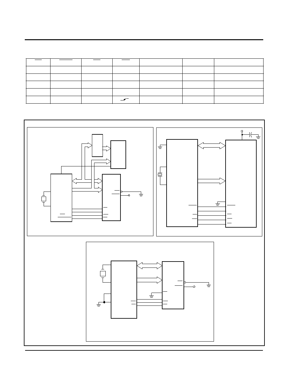
CONTROL
LOGIC
INDIVIDUALLY LOCKABLE
D
E
C
O
D
E
R
L
A
T
C
H
A/D
0
≠A/D
7
A
8
≠A
12
INTERFACE
WR
RD
PSEN
CE
WC
CONTROL
SOFTWARE DATA PROTECT
(SDP)
POWER-ON RESET
AND V
CC
SENSE
WE
OE
BUS TRANSCEIVER
A/D
0
≠A/D
7
1Kx8 BLOCKS
ALE
BLOCK LOCK
E
2
PROM
ARRAY
A
PPLICATION
N
OTE
A V A I L A B L E
Application Brief

X88064
2
Pin configuration
PIN NAMES
PIN NAME
I/O
DESCRIPTION
PSEN
I
Content of E
2
memory can be read by lowering the PSEN and holding both RD and WR
HIGH. The device then places on the data bus (AD
0
≠AD
7
) the contents of E
2
memory at the
latched address.
A
8
≠A
12
I
Non-multiplexed high-order Address Bus inputs for the upper byte of the address.
AD
0
≠AD
7
I/O
Multiplexed low-order Address and Data Bus. The addresses are latched when ALE makes a
HIGH to LOW transition.
WR
I
During a byte/page write cycle WR is brought LOW while RD is held HIGH and the data is
placed on the bus. The rising edge of
WR
latches data into the device.
RD
I
The RD input is active LOW and is used to read content of the E
2
memory at the latched
address. Both PSEN an WR signals must be held HIGH during RD controlled read operation.
WC
I
WC input has to be held LOW during a write cycle. It can be permanently tied HIGH in order
to disable write to the E
2
memory. Taking WC HIGH prior to t
BLC
(100ns, the time delay from
the last write cycle to the start of internal programming cycle) will inhibit the write operation.
CE
I
The device select (CE) is an active LOW input. This signal has to be asserted prior to ALE
HIGH to LOW transition in order to generate a valid internal device select signal. Holding this
pin HIGH and ALE LOW will place the device in standby mode.
ALE
I
Address Latch Enable input is used to latch the addresses present on the address lines
A
8
≠A
12
and AD
0
≠AD
7
into the device. The addresses are latched when ALE transitions from
HIGH to LOW.
7023 FRM F02
NC
A
12
NC
NC
WC
PSEN
A/D
0
A/D
1
A/D
2
A/D
3
A/D
4
V
SS
1
2
3
4
5
6
7
8
9
10
11
12
24
23
22
21
20
19
18
17
16
15
14
13
V
CC
WR
ALE
A
8
A
9
A
11
RD
A
10
CE
A/D
7
A/D
6
A/D
5
X88064
DIP/SOIC
Software Data Program Control provides a lower level of
memory write management. SDP controls write opera-
tions to the entire memory. When enabled, the host micro-
processor must send a special 3 byte command sequence
before any byte or page writes to unlocked locations in the
memory.

X88064
3
PRINCIPLES OF OPERATION
The X88064 is a highly integrated peripheral device for a
wide variety of single-chip microcontrollers. The X88064
provides 8K bytes of E
2
PROM which can be used either
for Program Storage, Data Storage, or a combination of
both, in systems based upon Harvard (80XX) architec-
tures. The X88064 incorporates the interface circuitry
normally needed to decode the control signals and
demultiplex the Address/Data bus to provide a "Seam-
less" interface.
The interface inputs on the X88064 are configured such
that it is possible to directly connect them to the proper
interface signals of the appropriate single-chip microcon-
troller. In the Harvard type system, the reading of data
from the chip is controlled either by the PSEN or the RD
signal, which essentially maps the X88064 into both the
Program and the Data Memory address map.
The X88064 also features an advanced implementation
of the Software Data Protection scheme, called Block
Lock, which allows the device to be broken into 8 inde-
pendent sections of 1K bytes. Each of these sections can
be independently enabled for write operations; thereby
allowing certain sections of the device to be secured so
that updates can only occur in a controlled environment
(e.g. in an automotive application, only at an authorized
service center). The desired set-up configuration is
stored in a nonvolatile register, ensuring the configuration
data will be maintained after the device is powered down.
The X88064 also features a Write Control input (WC),
which serves as an external control over the completion
of a previously initiated page load cycle.
The X88064 also features the industry standard
E
2
PROM characteristics such as byte or page mode
write and Toggle Bit Polling.
DEVICE OPERATION MODES
Mixed Program/Data Memory
By properly assigning the address space, a single
X88064 can be used as both the Program and Data
Memory. This would be accomplished by connecting all
of the Microcontroller control outputs to the correspond-
ing inputs of the X88064.
The Data Storage can be fully protected by enabling
Block Lock Control.
Program Memory Mode
This mode of operation is read-only. The PSEN and ALE
inputs of the X88064 are tied directly to the PSEN and
ALE outputs of the microcontroller. The RD and WR
inputs are tied HIGH.
When ALE is HIGH, the A/D
0
≠A/D
7
and A
8
≠A
12
addresses flow into the device. The addresses, both low
and high order, are latched when ALE transitions LOW
(V
IL
). PSEN will then go LOW and after t
PLDV
, valid data
is presented on the A/D
0
≠A/D
7
pins. CE must be LOW
during the entire operation.
Data Memory Mode
This mode of operation allows both read and write func-
tions. The PSEN input is tied to V
IH
or to V
CC
through a
pull-up resistor. The ALE, RD, and WR inputs are tied
directly to the microcontroller's ALE, RD, and WR out-
puts.
Read
This operation is quite similar to the Program Memory
read. A HIGH to LOW transition on ALE latches the
addresses and the data will be output on the A/D pins
after RD goes LOW (t
RLDV
).
Write
A write is performed by latching the addresses on the fall-
ing edge of ALE. Then WR is strobed LOW followed by
valid data being presented at the A/D
0
≠A/D
7
pins. The
data will be latched into the X88064 on the rising edge of
WR. To write to the X88064, with the SDP feature
enabled, a three-byte command sequence must precede
the byte(s) being written. (See Software Data Protec-
tion.)
X88064
4
MODE SELECTION
7023 FRM T02
CE
PSEN
RD
WR
Mode
I/O
Power
V
CC
X
X
X
Standby
High Z
Standby (CMOS)
HIGH
X
X
X
Standby
High Z
Standby (TTL)
LOW
LOW
HIGH
HIGH
Program Fetch
D
OUT
Active
LOW
HIGH
LOW
HIGH
Data Read
D
OUT
Active
LOW
HIGH
HIGH
Write
D
IN
Active
TYPICAL APPLICATIONS
A
8
≠
A
12
WC
PSEN
ALE
RD
WR
CE
V
CC
PSEN
ALE
RD
WR
P2.7
80C51
µ
C Family
EA/VP
X1
X2
X88064
196 Interface
188 Interface
7023 FRM F03
X1
EA
A/D
0
≠
A/D
7
A/D
8
≠
A/D
15
ALE
WR
RD
U2
8X196 KC/KD
A/D
0
≠
A/D
7
CE
WC
PSEN
VCC
X88064
BUSWIDTH
ALE
WR
RD
X2
A
8
≠
A
12
U1
X1
A/D
0
≠
A/D
7
A/D
8
≠
A/D
15
ALE/QS0
WR/QS1
RD/QSMD
U2
A/D
0
≠
A/D
7
WC
PSEN
VCC
X88064
ALE
WR
RD
X2
A
8
≠
A
12
U1
UCS
CE
RAM
LATCH
U4
U3
80188
LCS
A/D
0
≠
A/D
7
A
8
≠
A
12
A/D
0
≠
A/D
7

X88064
5
PAGE WRITE OPERATION
Regardless of the microcontroller employed, the X88064
supports page mode write operations. This allows the
microcontroller to write from one to thirty-two bytes of
data to the X88064. Each individual write within a page
write operation must conform to the byte write timing
requirements. The falling edge of WR starts a timer
delaying the internal programming cycle 100
µ
s. There-
fore, each successive write operation must begin within
100
µ
s of the last byte written. The following waveforms
illustrate the sequence and timing requirements.
Page Write Timing Sequence for WR Controller Operation
Notes:
(1) For each successive write within a page write cycle A
5
≠A
12
must be the same.
t
BLC
CE
ALE
A/D
0
≠A/D
7
A
8
≠A
12
WR
PSEN(RD)
A
IN
D
IN
A12=n
OPERATION
BYTE 0
BYTE 1
BYTE 2
LAST BYTE
READ (1)
AFTER t
WC
READY FOR
NEXT WRITE OPERATION
t
WC
7023 FRM F04
A
IN
D
IN
A12=n
A
IN
D
IN
A12=n
A
IN
D
IN
A12=n
A
IN
D
OUT
A12=x
A
IN
ADDR
A
IN
Next Address

X88064
6
TOGGLE BIT POLLING
Because the X88064 typical nonvolatile write cycle time
is less than the specified 5ms, Toggle Bit Polling has
been provided to determine the early completion of write.
During the internal programming cycle I/O
6
will toggle
from HIGH to LOW and LOW to HIGH on subsequent
attempts to read the device. When the internal cycle is
complete, the toggling will cease and the device will be
accessible for additional read or write operations.
Toggle Bit Polling RD/WR Control
Symbol Table
RD
LAST BYTE ∑
WRITTEN
CE
ALE
A/D
0
≠A/D
7
A
8
≠A
12
WR
AIN
D IN
OPERATION
AIN
DOUT
AIN
DOUT
AIN
DOUT
AIN
D OUT
AIN
ADDR
I/O6=X
X88064 READ Y FOR
NEXT OPERATION
7023 FRM F05
I/O6=X
I/O6=X
I/O6=X
A12=n
A12=n
A12=n
A12=n
A12=n
WAVEFORM
INPUTS
OUTPUTS
Must be
steady
Will be
steady
May change
from LOW
to HIGH
Will change
from LOW
to HIGH
May change
from HIGH
to LOW
Will change
from HIGH
to LOW
Don't Care:
Changes
Allowed
Changing:
State Not
Known
N/A
Center Line
is High
Impedance
X88064
7
DATA PROTECTION
The X88064 provides two levels of data protection
through software control. There is a global software data
protection feature similar to the industry standard for
E
2
PROMs and a new Block Lock Control providing a
secondary level of data security.
SOFTWARE DATA PROTECTION
The X88064 offers a software controlled data protection
feature. The X88064 is shipped from Xicor with the soft-
ware data protection NOT ENABLED; that is, the device
will be in the standard operating mode. In this mode data
should be protected during power-up/down operations
through the use of external circuits. The host then has
open read and write access of the device once V
CC
is
stable.
The X88064 can be automatically protected during
power-up/down without the need for external circuits by
employing the software data protection feature. The inter-
nal software data protection circuit is enabled after the
first write operation utilizing the software algorithm. This
circuit is nonvolatile and will remain set for the life of the
device unless the SDP deactivation command is issued.
Once the software protection is enabled, the X88064 is
also protected from inadvertent and accidental writes in
the powered-up state. That is, the SDP software algo-
rithm must be issued prior to writing additional data to the
device.
Writing with SDP Enabled
SEQUENCE TO DEACTIVATE SOFTWARE DATA
PROTECTION
WRITE AA
TO X555
WRITE 55
TO XAAA
WRITE A0
TO X555
PERFORM BYTE
OR PAGE WRITE
OPERATIONS
WAIT t
WC
EXIT ROUTINE
X = Address bit (A12) of
7023 FRM F06
the byte being updated.
WRITE AA to 555
EXIT ROUTINE
WRITE 55 to AAA
WRITE A0 to 555
WRITE AA to 555
WRITE 80 to AAA
WAIT OF t
wc

X88064
8
Block Lock Write Control
The X88064 provides a secondary level of data security
referred to as Block Lock Control. This is accessed
through an extension of the SDP command sequence.
Block Lock allows the user to inhibit writes to any 1K x 8
blocks of memory. Unlike SDP which prevents inadvert-
ent writes, but still allows easy system access to writing
the memory, Block Lock will inhibit all attempts unless it is
specifically disabled by the host. This could be used to
set a higher level of protection in a system where a por-
tion of the memory is used for Program Storage and
another portion is used as Data Storage.
Setting write lockout is accomplished by writing a five-
byte command sequence, opening access to the Block
Lock Register (BLR). After the fifth byte is written, the
user writes to the BLR, selecting which blocks to protect
or unprotect. All write operations, both the command
sequence and writing the data to the BLR, must conform
to the page write timing requirements.
Block Lock Register Format
Setting Block Lock Register Sequence
6
5
4
3
2
1
0
7
0000≠03FF
0400≠07FF
0800≠0BFF
0C00≠0FFF
1000≠13FF
1400≠17FF
1800≠1BFF
1C00≠1FFF
BLOCK
ADDRESS
1 = Locked, 0 = Unlocked
MSB
LSB
7023 FRM F07
WRITE AA
TO 555
WRITE BLR
MASK VALUE TO
XXXX
WAIT t
WC
WRITE 55
TO AAA
WRITE C0
TO AAA
(BLR SET)
7023 FRM F08
WRITE AA
TO 555
WRITE A0
TO 555
EXIT ROUTINE

X88064
9
D.C. OPERATING CHARACTERISTICS (Over recommended operating conditions unless otherwise specified.)
7023 FRM T05
CAPACITANCE T
A
= +25
∞
C, f = 1MHz, V
CC
= 5V
7023 FRM T06
POWER-UP TIMING
7032 FRM T07
Notes: (3) V
IL
min. and V
IH
max. are for reference only and are not tested.
(4) This parameter is periodically sampled and not 100% tested.
Limits
Symbol
Parameter
Min.
Max.
Units
Test Conditions
I
CC
V
CC
Current (Active)
30
mA
CE = RD = V
IL
, All I/O's = Open,
Other Inputs = V
CC
I
SB1(CMOS)
V
CC
Current (Standby)
150
µ
A
CE = V
CC
≠ 0.3V,
All I/O's = Open,
Other Inputs = V
CC
≠ 0.3V, ALE = V
IL
I
SB2(TTL)
V
CC
Current (Standby)
2.5
mA
CE = V
IH
, All I/O's = Open,
Other Inputs = V
IH
, ALE = V
IL
I
LI
Input Leakage Current
10
µ
A
V
IN
= V
SS
to V
CC
I
LO
Output Leakage Current
10
µ
A
V
OUT
= V
SS
to V
CC
, RD = V
IH
= PSEN
V
lL(3)
Input LOW Voltage
≠1
0.8
V
V
IH(3)
Input HIGH Voltage
2
V
CC
+ 0.5
V
V
OL
Output LOW Voltage
0.4
V
I
OL
= 2.1 mA
V
OH
Output HIGH Voltage
2.4
V
I
OH
= ≠400
µ
A
Symbol
Test
Max.
Units
Conditions
C
I/O(4)
Input/Output Capacitance
10
pF
V
I/O
= 0V
C
IN(4)
Input Capacitance
6
pF
V
IN
= 0V
Symbol
Parameter
Max.
Units
t
PUR(4)
Power-Up to Read
1
ms
t
PUW(4)
Power-Up to Write
5
ms
ABSOLUTE MAXIMUM RATINGS*
Temperature under Bias.......................≠65
∞
C to +135
∞
C
Storage Temperature ...........................≠65
∞
C to +150
∞
C
Voltage on any Pin with
Respect to V
SS
.......................................... ≠1V to +7V
D.C. Output Current.................................................5 mA
Lead Temperature
(Soldering, 10 seconds)300
∞
C
*COMMENT
Stresses above those listed under "Absolute Maximum Rat-
ings" may cause permanent damage to the device. This is a
stress rating only and the functional operation of the device
at these or any other conditions above those indicated in the
operational sections of this specification is not implied. Ex-
posure to absolute maximum rating conditions for extended
periods may affect device reliability.
RECOMMENDED OPERATING CONDITIONS
7023 FRM T03
7023 FRM T04
Temperature
Min.
Max.
Commercial
0
∞
C
+70
∞
C
Industrial
≠40
∞
C
+85
∞
C
Supply Voltage
Limits
X88064
5V
±
10%
X88064-60
5V
±
10%
X88064
10
PSEN Controlled Read Cycle
7023 FRM T09
PSEN Controlled Read Timing Diagram
X88064 ≠ 60
X88064
Symbol
Parameter
Min.
Max.
Min.
Max.
Units
t
LHLL
ALE Pulse Width
60
80
ns
t
AVLL
Address Setup Time
10
10
ns
t
LLAX
Address Hold Time
20
20
ns
t
PLDV
PSEN Read Access Time
45
80
ns
t
PHDX
Data Hold Time
0
0
ns
t
ELLL
Chip Enable Setup Time
7
7
ns
PW
PL
PSEN Pulse Width
100
140
ns
t
PS
PSEN Setup Time
20
30
ns
t
PH
PSEN Hold Time
20
20
ns
t
PHDZ
(5)
PSEN Disable to Output in High Z
20
30
ns
t
PLDX
(5)
PSEN to Output in Low Z
10
10
ns
ALE
A/D
0
≠A/D
7
A
8
≠A
12
PSEN
A
IN
t
PLDV
D
OUT
7023 FRM F10
t
PH
t
PH
t
LHLL
t
AVLL
t
LLAX
t
PS
P
WPL
ADDRESS
CE
t
PLDX
t
PHDZ
t
PHDX
t
ELLL
A.C. CONDITIONS OF TEST
7023 FRM T08
Input Pulse Levels
0V to 3V
Input Rise and Fall Times
10ns
Input and Output Timing Levels
1.5V
7023 FRM F09
5V
1.92K
100pF
OUTPUT
1.37K
EQUIVALENT A.C. TEST CIRCUIT
X88064
11
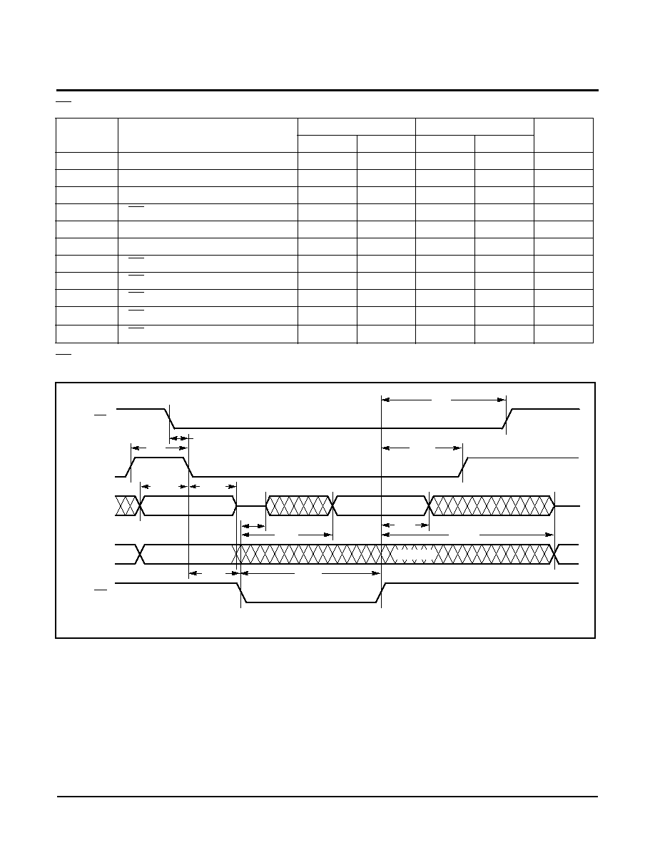
RD Controlled Read Cycle
7023 FRM T10
RD Controlled Read Timing Diagram
Notes: (6) This parameter is periodically sampled and not 100% tested.
X88064 ≠ 60
X88064
Symbol
Parameter
Min.
Max.
Min.
Max.
Units
t
LHLL
ALE Pulse Width
60
80
ns
t
AVLL
Address Setup Time
10
10
ns
t
LLAX
Address Hold Time
20
20
ns
t
RLDV
RD Read Access Time
60
80
ns
t
RHDX
Data Hold Time
0
0
ns
t
ELLL
Chip Enable Setup Time
7
7
ns
PW
RL
RD Pulse Width
120
150
ns
t
RDS
RD Setup Time
20
30
ns
t
RDH
RD Hold Time
20
20
ns
t
RHDZ
(6)
RD Disable to Output in High Z
20
30
ns
t
RLDX
(6)
RD to Output in Low Z
0
0
ns
ALE
A/D
0
≠A/D
7
A
8
≠A
12
RD
A
IN
t
RLDV
D
OUT
7023 FRM F11
t
RDH
t
RDH
t
LHLL
t
AVLL
t
LLAX
t
RDS
PW
RL
ADDRESS
CE
t
RLDX
t
RHDZ
t
RHDX
t
ELLL

X88064
12
WR Controlled Write Cycle
7023 FRM T11
WR Controlled Write Timing Diagram
Notes: (7) TWC is the minimum cycle time to be allowed from the system perspective unless polling techniques are used. It is the maximum time
the device requires to automatically complete the internal write operation.
X88064 ≠ 60
X88064
Symbol
Parameter
Min.
Max.
Min.
Max.
Units
t
LHLL
ALE Pulse Width
60
80
ns
t
AVLL
Address Setup Time
10
10
ns
t
LLAX
Address Hold Time
20
20
ns
t
DVWH
Data Setup Time
50
50
ns
t
WHDX
Data Hold Time
30
30
ns
t
ELLL
Chip Enable Setup Time
7
7
ns
t
WLWH
WR Pulse Width
100
120
ns
t
WRS
WR Setup Time
20
30
ns
t
WRH
WR Hold Time
20
20
ns
t
BLC
Byte Load Time (Page Write)
0.5
100
0.5
100
µ
s
t
WC (7)
Write Cycle Time
5
5
ms
ALE
A/D
0
≠A/D
7
A
8
≠A
12
WR
A
IN
t
DVWH
D
IN
t
WHDX
t
WRH
t
WRH
t
LHLL
t
AVLL
t
LLAX
t
WRS
t
WLWH
ADDRESS
CE
t
ELLL
7023 FRM T12

X88064
13
PACKAGING INFORMATION
7023 FRM F13
NOTE:
1. ALL DIMENSIONS IN INCHES (IN PARENTHESES IN MILLIMETERS)
2. PACKAGE DIMENSIONS EXCLUDE MOLDING FLASH
0.022 (0.56)
0.014 (0.36)
0.150 (3.81)
0.125 (3.18)
0.625 (15.87)
0.600 (15.24)
0.110 (2.79)
0.090 (2.29)
1.265 (32.13)
1.230 (31.24)
1.100 (27.94)
REF.
PIN 1 INDEX
0.162 (4.11)
0.140 (3.56)
0.030 (0.76)
0.015 (0.38)
PIN 1
SEATING
PLANE
0.065 (1.65)
0.040 (1.02)
0.557 (14.15)
0.530 (13.46)
0.080 (2.03)
0.065 (1.65)
0
∞
15
∞
24-LEAD PLASTIC DUAL IN-LINE PACKAGE TYPE P
TYP. 0.010 (0.25)

X88064
14
PACKAGING INFORMATION
0.290 (7.37)
0.299 (7.60)
0.393 (10.00)
0.420 (10.65)
0.014 (0.35)
0.020 (0.50)
PIN 1
PIN 1 INDEX
0.050 (1.27)
0.598 (15.20)
0.610 (15.49)
0.003 (0.10)
0.012 (0.30)
0.092 (2.35)
0.105 (2.65)
(4X) 7
∞
7023 FRM F14
24-LEAD PLASTIC SMALL OUTLINE GULL WING PACKAGE TYPE S
NOTE: ALL DIMENSIONS IN INCHES (IN PARENTHESES IN MILLIMETERS)
0.420"
0.050" TYPICAL
0.050"
TYPICAL
0.030" TYPICAL
24 PLACES
FOOTPRINT
0.010 (0.25)
0.020 (0.50)
0.015 (0.40)
0.050 (1.27)
0.009 (0.22)
0.013 (0.33)
0
∞
≠ 8
∞
X 45
∞

X88064
15
ORDERING INFORMATION
Device
X88064
X
X
Temperature Range
Blank = Commercial = 0
∞
C to +70
∞
C
I = Industrial = ≠40
∞
C to +85
∞
C
LIMITED WARRANTY
Devices sold by Xicor, Inc. are covered by the warranty and patent indemnification provisions appearing in its Terms of Sale only. Xicor, Inc.
makes no warranty, express, statutory, implied, or by description regarding the information set forth herein or regarding the freedom of the
described devices from patent infringement. Xicor, Inc. makes no warranty of merchantability or fitness for any purpose. Xicor, Inc. reserves the
right to discontinue production and change specifications and prices at any time and without notice.
Xicor, Inc. assumes no responsibility for the use of any circuitry other than circuitry embodied in a Xicor, Inc. product. No other circuits, patents,
licenses are implied.
U.S. PATENTS
Xicor products are covered by one or more of the following U.S. Patents: 4,263,664; 4,274,012; 4,300,212; 4,314,265; 4,326,134; 4,393,481;
4,404,475; 4,450,402; 4,486,769; 4,488,060; 4,520,461; 4,533,846; 4,599,706; 4,617,652; 4,668,932; 4,752,912; 4,829, 482; 4,874, 967;
4,883, 976. Foreign patents and additional patents pending.
LIFE RELATED POLICY
In situations where semiconductor component failure may endanger life, system designers using this product should design the system with
appropriate error detection and correction, redundancy and back-up features to prevent such an occurence.
Xicor's products are not authorized for use in critical components in life support devices or systems.
1. Life support devices or systems are devices or systems which, (a) are intended for surgical implant into the body, or (b) support or sustain
life, and whose failure to perform, when properly used in accordance with instructions for use provided in the labeling, can be reasonably
expected to result in a significant injury to the user.
2. A critical component is any component of a life support device or system whose failure to perform can be reasonably expected to cause the
failure of the life support device or system, or to affect its safety or effectiveness.
Packages:
P = 24-Lead Plastic DIP
S = 24-Lead SOIC
XX
Access Time
Blank = 80 ns
-60 = 60 ns