 | –≠–ª–µ–∫—Ç—Ä–æ–Ω–Ω—ã–π –∫–æ–º–ø–æ–Ω–µ–Ω—Ç: X88C64SI | –°–∫–∞—á–∞—Ç—å:  PDF PDF  ZIP ZIP |
Document Outline
- Table of Contents
- Product Selection
- Data Sheet Alpha
- Ap Note Alpha

X88C64
1
© Xicor, Inc. 1994, 1995, 1996 Patents Pending
Characteristics subject to change without notice
3867-1.5 7/9/96 T0/C2/D0 NS
E
2
Micro-Peripheral
3867 FHD F02
8051 Microcontroller Family Compatible
CONCURRENT READ WRITE
TM
is a trademark of Xicor, Inc.
DESCRIPTION
The X88C64 is an 8K x 8 E
2
PROM fabricated with
advanced CMOS Textured Poly Floating Gate Tech-
nology. The X88C64 features a Multiplexed Address
and Data bus allowing a direct interface to a variety of
popular single-chip microcontrollers operating in ex-
panded multiplexed mode without the need for addi-
tional interface circuitry.
The X88C64 is internally configured as two indepen-
dent 4K x 8 memory arrays. This feature provides the
ability to perform nonvolatile memory updates in one
array and continue operation out of code stored in the
other array; effectively eliminating the need for an
auxiliary memory device for code storage.
To write to the X88C64, a three-byte command
sequence must precede the byte(s) being written. The
X88C64 also provides a second generation software
data protection scheme called Block Protect. Block
Protect can provide write lockout of the entire device
or selected 1K blocks. There are eight 1K x 8 blocks
that can be write protected individually in any combi-
nation required by the user. Block Protect, in addition
to Write Control input, allows the different segments
of the memory to have varying degrees of alterability
in normal system operation.
FEATURES
∑
CONCURRENT READ WRITE
TM
--Dual Plane Architecture
--Isolates Read/Write Functions
Between Planes
--Allows Continuous Execution of Code
From One Plane While Writing in
the Other Plane
∑
Multiplexed Address/Data Bus
--Direct Interface to Popular 8051 Family
∑
High Performance CMOS
--Fast Access Time, 120ns
--Low Power
--60mA Active Maximum
--500
µ
A Standby Maximum
∑
Software Data Protection
∑
Block Protect Register
--Individually Set Write Lock Out in 1K Blocks
∑
Toggle Bit Polling
--Early End of Write Detection
∑
Page Mode Write
--Allows up to 32 Bytes to be Written in
One Write Cycle
∑
High Reliability
--Endurance: 100,000 Write Cycle
--Data Retention: 100 Years
CONTROL
LOGIC
SOFTWARE
DATA
PROTECT
CE
WR
RD
PSEN
A8≠A11
ALE
L
A
T
C
H
E
S
D
E
C
O
D
E
A12
A12
M
U
X
1K BYTES
1K BYTES
1K BYTES
1K BYTES
Y DECODE
I/O & ADDRESS LATCHES AND BUFFERS
A/D0≠A/D7
WC
1K BYTES
1K BYTES
1K BYTES
1K BYTES
A12
X
FUNCTIONAL DIAGRAM
S L I C
64K
X88C64
8192 x 8 Bit
A
PPLICATION
N
OTE
A V A I L A B L E
AN63
X88C64
2
PIN DESCRIPTIONS
Address/Data (A/D
0
≠A/D
7
)
Multiplexed low-order addresses and data. The Ad-
dresses flow into the device while ALE is HIGH. After
ALE transitions from a HIGH to LOW the addresses
are latched. Once the addresses are latched these
pins input data or output data depending on
RD
,
WR
,
PSEN
, and
CE
.
Addresses (A
8
≠A
12
)
High order addresses flow into the device when ALE
is HIGH and are latched when ALE goes LOW.
Chip Enable (
CE
)
The Chip Enable input must be LOW to enable all
read/write operations. When
CE
is HIGH and ALE is
LOW, the X88C64 is placed in the low power standby
mode.
Program Store Enable (
PSEN
)
When the X88C64 is to be used in a 8051 based
system,
PSEN
is tied directly to the microcontroller's
PSEN
output.
Read (
RD
)
When the X88C64 is to be used in a 8051 based
system,
RD
is tied directly to the microcontroller's
RD
output.
Write (
WR
)
When the X88C64 is to be used in a 8051 based
system,
WR
is tied directly to the microcontroller's
WR
output.
Address Latch Enable (ALE)
Addresses flow through the latches to address de-
coders when ALE is HIGH and are latched when ALE
transitions from a HIGH to LOW.
Write Control (
WC
)
The Write Control allows external circuitry to abort a
page load cycle once it has been initiated. This input
is useful in applications in which a power failure or
processor RESET could interrupt a page load cycle.
In this case, the microcontroller might drive all signals
HIGH, causing bad data to be latched into the
E
2
PROM. If the Write Control input is driven HIGH
(before t
BLC
Max) after Write (
WR
) goes HIGH, the
write cycle will be aborted.
When
WC
is LOW (tied to V
SS
) the X88C64 will be
enabled to perform write operations. When
WC
is
HIGH normal read operations may be performed, but
all attempts to write to the device will be disabled.
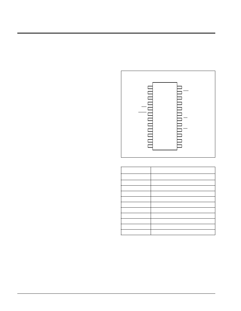
PIN CONFIGURATION
3867 FHD F01
PIN NAMES
Symbol
Description
ALE
Address Latch Enable
A/D
0
≠A/D
7
Address Inputs/Data I/O
A
8
≠A
12
Address Inputs
RD
Read Input
WR
Write Input
PSEN
Program Store Enable Input
CE
Chip Enable
WC
Write Control
V
SS
Ground
V
CC
Supply Voltage
NC
No Connect
3867 PGM T01.1
NC
A12
NC
NC
WC
PSEN
A/D0
A/D1
A/D2
A/D3
A/D4
VSS
1
2
3
4
5
6
7
8
9
10
11
12
24
23
22
21
20
19
18
17
16
15
14
13
VCC
WR
ALE
A8
A9
A11
RD
A10
CE
A/D7
A/D6
A/D5
X88C64
DIP/SOIC
X88C64
3
PRINCIPLES OF OPERATION
The X88C64 is a highly integrated peripheral device for
a wide variety of single-chip microcontrollers. The
X88C64 provides 8K bytes of E
2
PROM which can be
used either for Program Storage, Data Storage, or a
combination of both in systems based upon Harvard
(80XX) architectures. The X88C64 incorporates the
interface circuitry normally needed to decode the control
signals and demultiplex the Address/Data bus to pro-
vide a "Seamless" interface.
The interface inputs on the X88C64 are configured such
that it is possible to directly connect them to the proper
interface signals of the appropriate single-chip
microcontroller. In the Harvard type system, the reading
of data from the chip is controlled either by the
PSEN
or
the
RD
signal, which essentially maps the X88C64 into
both the Program and the Data Memory address map.
The X88C64 is internally organized as two independent
planes of 4K bytes of memory with the A
12
input select-
ing which of the two planes of memory are to be
accessed. While the processor is executing code out of
one plane, write operations can take place in the other
plane, allowing the processor to continue execution of
code out of the X88C64 during a byte or page write to the
device.
The X88C64 also features an advanced implementation
of the Software Data Protection scheme, called Block
Protect, which allows the device to be broken into 8
independent sections of 1K bytes. Each of these sec-
tions can be independently enabled for write operations;
thereby allowing certain sections of the device to be
secured so that updates can only occur in a controlled
environment (e.g. in an automotive application, only at
an authorized service center). The desired set-up con-
figuration is stored in a nonvolatile register, ensuring the
configuration data will be maintained after the device is
powered down.
The X88C64 also features a Write Control input (
WC
),
which serves as an external control over the completion
of a previously initiated page load cycle.
The X88C64 also features the industry standard
E
2
PROM characteristics such as byte or page mode
write and Toggle Bit Polling.
DEVICE OPERATION
MODES
Mixed Program/Data Memory
By properly assigning the address spaces, a single
X88C64 can be used as both the Program and Data
Memory. This would be accomplished by connecting all
of the 8051 control outputs to the corresponding inputs
of the X88C64.
In this configuration, one plane of memory could be
dedicated to Program Storage and the other plane
dedicated to Data Storage. The Data Storage can be
fully protected by enabling block protect write lockout.
Program Memory Mode
This mode of operation is read-only. The
PSEN
and
ALE
inputs of the X88C64 are tied directly to the
PSEN
and
ALE outputs of the microcontroller. The
RD
and
WR
inputs are tied HIGH.
When ALE is HIGH, the A/D
0
≠A/D
7
and A
8
≠A
12
ad-
dresses flow into the device. The addresses, both low
and high order, are latched when ALE transitions LOW
(V
IL
).
PSEN
will then go LOW and after t
PLDV
, valid data
is presented on the A/D
0
≠A/D
7
pins.
CE
must be LOW
during the entire operation.
3867 FHD F03
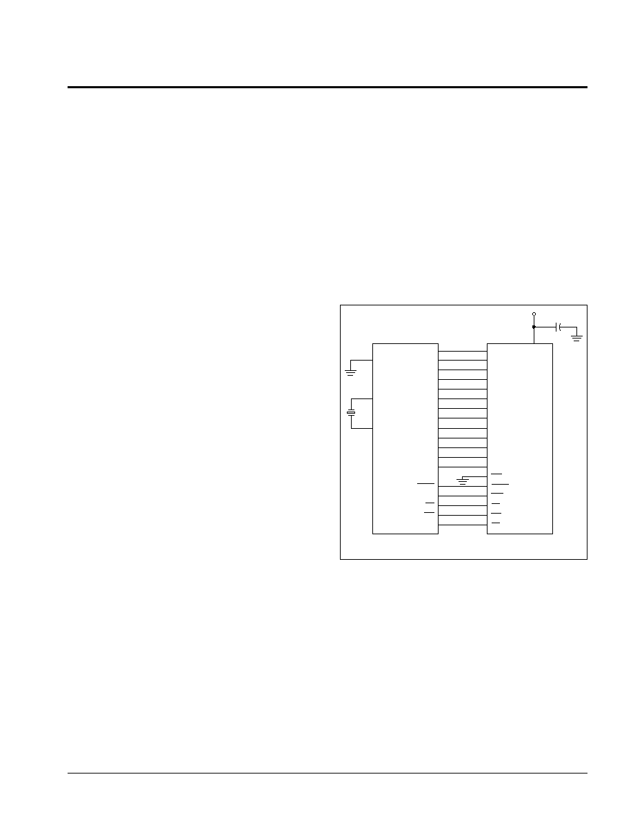
TYPICAL APPLICATION
P0.0
P0.1
P0.2
P0.3
P0.4
P0.5
P0.6
P0.7
P2.0
P2.1
P2.2
P2.3
P2.4
PSEN
ALE
RD
WR
P2.7
39
38
37
36
35
34
33
32
21
22
23
24
25
29
30
17
16
7
8
9
10
11
13
14
15
21
20
17
19
2
5
6
22
18
23
16
A/D0
A/D1
A/D2
A/D3
A/D4
A/D5
A/D6
A/D7
A8
A9
A10
A11
A12
WC
PSEN
ALE
RD
WR
CE
VCC
24
X1
X2
EA/VP
31
19
18
X88C64
80C31
X88C64
4
Data Memory Mode
This mode of operation allows both read and write
functions. The
PSEN
input is tied to V
IH
or to V
CC
through a pull-up resistor. The ALE,
RD
, and
WR
inputs
are tied directly to the microcontroller's ALE,
RD
, and
WR
outputs.
Read
This operation is quite similar to the Program Memory
read. A HIGH to LOW transition on ALE latches the
addresses and the data will be output on the AD pins
after
RD
goes LOW (t
RLDV
).
Write
A write is performed by latching the addresses on the
falling edge of ALE. Then
WR
is strobed LOW followed
by valid data being presented at the A/D
0
≠A/D
7
pins.
The data will be latched into the X88C64 on the rising
edge of
WR
. To write to the X88C64, a three-byte
command sequence must precede the byte(s) being
written. (See Software Data Protection.)
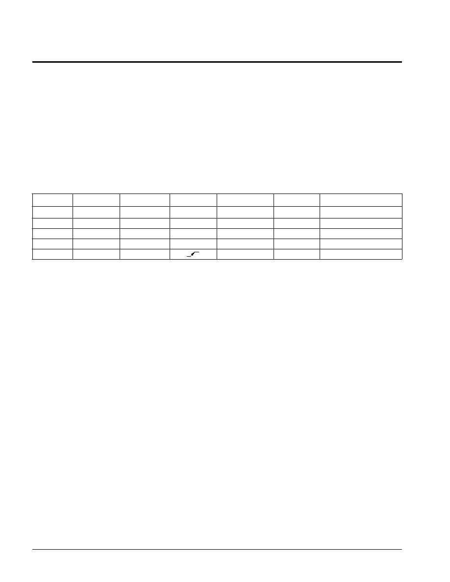
MODE SELECTION
CE
PSEN
RD
WR
Mode
I/O
Power
V
CC
X
X
X
Standby
High Z
Standby (CMOS)
HIGH
X
X
X
Standby
High Z
Standby (TTL)
LOW
LOW
HIGH
HIGH
Program Fetch
D
OUT
Active
LOW
HIGH
LOW
HIGH
Data Read
D
OUT
Active
LOW
HIGH
HIGH
Write
D
IN
Active
3867 PGM T02.2
X88C64
5
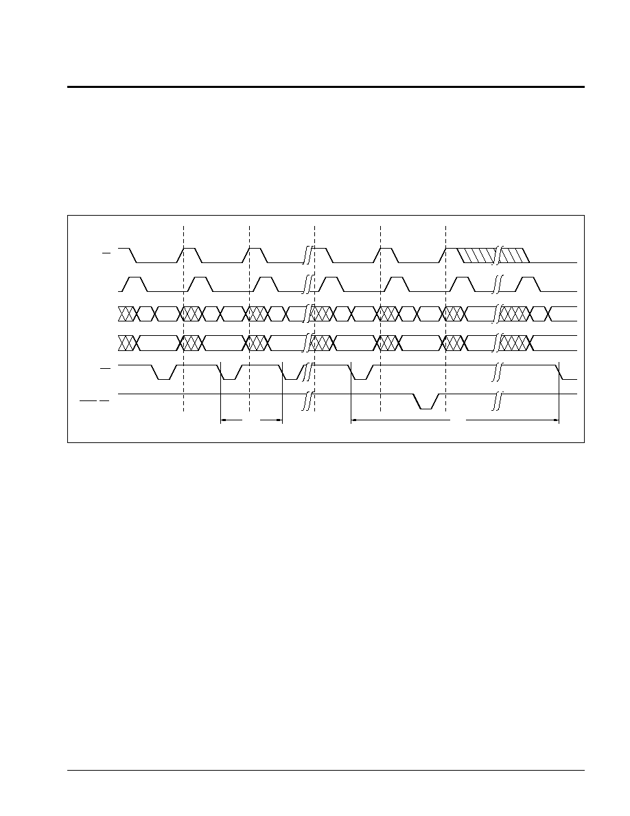
Page Write Timing Sequence for
WR
Controlled Operation
Notes: (1) For each successive write within a page write cycle A
5
≠A
12
must be the same.
(2) Although it is not illustrated, the microcontroller may interleave read operations between the individual byte writes within the page
write operation. Two responses are possible:
a. Reading from the same plane being written (A
12
of Read = A
12
of Write) is effectively a Toggle Bit Polling operation.
b. Reading from the opposite plane being written (A
12
of Read
A
12
of Write) true data will be returned, facilitating the use of a
single memory component as both program and data storage.
PAGE WRITE OPERATION
Regardless of the microcontroller employed, the X88C64
supports page mode write operations. This allows the
microcontroller to write from one to thirty-two bytes of
data to the X88C64. Each individual write within a page
write operation must conform to the byte write timing
requirements. The falling edge of
WR
starts a timer
delaying the internal programming cycle 100
µ
s. There-
fore, each successive write operation must begin within
100
µ
s of the last byte written. The following waveforms
illustrate the sequence and timing requirements.
3867 FHD F08
tBLC
CE
ALE
A/D0≠A/D7
A8≠A12
WR
PSEN(RD)
AIN
DIN
A12=n
OPERATION
BYTE 0
BYTE 1
BYTE 2
LAST BYTE
READ (1)(2)
AFTER tWC READY FOR
NEXT WRITE OPERATION
tWC
AIN
DIN
A12=n
AIN
DIN
A12=n
AIN
DIN
A12=n
AIN DOUT
A12=x
AIN
ADDR
AIN
Next Address
X88C64
6
Toggle Bit Polling
RD
/
WR
Control
TOGGLE BIT POLLING
Because the X88C64 typical nonvolatile write cycle time
is less than the specified 5ms, Toggle Bit Polling has
been provided to determine the early completion of
write. During the internal programming cycle I/O
6
will
toggle from HIGH to LOW and LOW to HIGH on subse-
quent attempts to read the device. When the internal
cycle is complete, the toggling will cease and the device
will be accessible for additional read or write operations.
Due to the dual plane architecture, reads for polling
must occur in the plane that was written; that is, the state
of A
12
during a write must match the state of A
12
during
Toggle Bit Polling.
3867 FHD F09
RD
LAST BYTE
WRITTEN
CE
ALE
A/D0≠A/D7
A8≠A12
WR
AIN
DIN
A12=n
OPERATION
AIN DOUT
A12=n
AIN DOUT
A12=n
AIN DOUT
A12=n
AIN DOUT
A12=x
AIN
ADDR
I/O6=X
X88C64 READY FOR
NEXT OPERATION
I/O6=X
I/O6=X
I/O6=X
SYMBOL TABLE
WAVEFORM
INPUTS
OUTPUTS
Must be
steady
Will be
steady
May change
from LOW
to HIGH
Will change
from LOW
to HIGH
May change
from HIGH
to LOW
Will change
from HIGH
to LOW
Don't Care:
Changes
Allowed
Changing:
State Not
Known
N/A
Center Line
is High
Impedance

X88C64
7
DATA PROTECTION
The X88C64 provides two levels of data protection
through software control. There is a global software data
protection feature similar to the industry standard for
E
2
PROMs and a new Block Protect write lockout protec-
tion providing a secondary level of data security.
SOFTWARE DATA PROTECTION
Software Data Protection (SDP) is employed to protect
the entire array against inadvertent writes. To write to the
X88C64, a three-byte command sequence must precede
the byte(s) being written. All write operations, both the
command sequence and any data write operations, must
conform to the page write timing requirements.
Setting write lockout is accomplished by writing a five-
byte command sequence, opening access to the Block
Protect Register (BPR). After the fifth byte is written, the
user writes to the BPR, selecting which blocks to protect
or unprotect. All write operations, both the command
sequence and writing the data to the BPR, must conform
to the page write timing requirements.
Block Protect Write Lockout
The X88C64 provides a secondary level of data security
referred to as Block Protect write lockout. This is ac-
cessed through an extension of the SDP command
sequence. Block Protect allows the user to lockout
writes to any 1K x 8 blocks of memory. Unlike SDP which
prevents inadvertent writes, but still allows easy system
access to writing the memory, Block Protect will lockout
all attempts unless it is specifically disabled by the host.
This could be used to set a higher level of protection in
a system where a portion of the memory is used for
Program Storage and another portion is used as Data
Storage.
Writing with SDP
3867 FHD F10
Block Protect Register Format
3867 FHD F12
6
5
4
3
2
1
0
7
0000≠03FF
0400≠07FF
0800≠0BFF
0C00≠0FFF
1000≠13FF
1400≠17FF
1800≠1BFF
1C00≠1FFF
BLOCK
ADDRESS
1 = Protect, 0 = Unprotect Block Specified
MSB
LSB
Setting BPR Sequence
3867 FHD F13
WRITE AA
TO X555
WRITE 55
TO XAAA
WRITE A0
TO X555
PERFORM BYTE
OR PAGE WRITE
OPERATIONS
WAIT tWC
EXIT ROUTINE
X = A
12
:
A12 = 1 IF DATA TO BE
WRITTEN IS WITHIN
ADDRESS 1000 TO 1FFF.
A12 = 0 IF DATA TO BE
WRITTEN IS WITHIN
ADDRESS 0000 TO 0FFF.
WRITE AA
TO X555
WRITE BPR
MASK VALUE TO
ANY ADDRESS
WAIT tWC
EXIT ROUTINE
WRITE 55
TO XAAA
WRITE C0
TO XAAA
(BPR REGISTER SET)
WRITE AA
TO X555
WRITE A0
TO X555
X = A
12
:
A
12
= 1 IF PROGRAM BEING EXECUTED
RESIDES WITHIN ADDRESS 0000 TO 0FFF.
A
12
= 0 IF PROGRAM BEING EXECUTED
RESIDES WITHIN ADDRESS 1000 TO 1FFF.

X88C64
8
*COMMENT
Stresses above those listed under "Absolute Maximum
Ratings" may cause permanent damage to the device.
This is a stress rating only and the functional operation of
the device at these or any other conditions above those
indicated in the operational sections of this specification is
not implied. Exposure to absolute maximum rating condi-
tions for extended periods may affect device reliability.
ABSOLUTE MAXIMUM RATINGS*
Temperature under Bias .................. ≠65
∞
C to +135
∞
C
Storage Temperature ....................... ≠65
∞
C to +150
∞
C
Voltage on any Pin with
Respect to V
SS
.................................. ≠1V to +7V
D.C. Output Current ............................................ 5 mA
Lead Temperature
(Soldering, 10 seconds) .............................. 300
∞
C
D.C. OPERATING CHARACTERISTICS (Over recommended operating conditions unless otherwise specified.)
Limits
Symbol
Parameter
Min.
Max.
Units
Test Conditions
I
CC
V
CC
Current (Active)
60
mA
CE
=
RD
= V
IL
, All I/O's =
Open,Other Inputs = V
CC
I
SB1(CMOS)
V
CC
Current (Standby)
500
µ
A
CE
= V
CC
≠ 0.3V,
All I/O's =
Open,Other Inputs = V
CC
≠
0.3V, ALE = V
IL
I
SB2(TTL)
V
CC
Current (Standby)
6
mA
CE
= V
IH
, All I/O's = Open, Other
Inputs = V
IH
, ALE = V
IL
I
LI
Input Leakage Current
10
µ
A
V
IN
= V
SS
to V
CC
I
LO
Output Leakage Current
10
µ
A
V
OUT
= V
SS
to V
CC
,
RD
= V
IH
=
PSEN
V
lL(3)
Input LOW Voltage
≠1
0.8
V
V
IH(3)
Input HIGH Voltage
2
V
CC
+ 0.5
V
V
OL
Output LOW Voltage
0.4
V
I
OL
= 2.1 mA
V
OH
Output HIGH Voltage
2.4
V
I
OH
= ≠400
µ
A
3867 PGM T05.2
Notes: (3) V
IL
min. and V
IH
max. are for reference only and are not tested.
(4) This parameter is periodically sampled and not 100% tested.
CAPACITANCE T
A
= +25
∞
C, f = 1MHz, V
CC
= 5V
Symbol
Test
Max.
Units
Conditions
C
I/O(4)
Input/Output Capacitance
10
pF
V
I/O
= 0V
C
IN(4)
Input Capacitance
6
pF
V
IN
= 0V
3867 PGM T06
POWER-UP TIMING
Symbol
Parameter
Max.
Units
t
PUR(4)
Power-Up to Read
1
ms
t
PUW(4)
Power-Up to Write
5
ms
3867 PGM T07
RECOMMENDED OPERATING CONDITIONS
Temperature
Min.
Max.
Commercial
0
∞
C
+70
∞
C
Industrial
≠40
∞
C
+85
∞
C
Military
≠55
∞
C
+125
∞
C
3867 PGM T03.1
Supply Voltage
Limits
X88C64
5V
±
10%
3867 PGM T04.1
X88C64
9
A.C. CONDITIONS OF TEST
Input Pulse Levels
0V to 3V
Input Rise and
Fall Times
10ns
Input and Output
Timing Levels
1.5V
3867 PGM T08.1
Note: (5) This parameter is periodically sampled and not 100% tested.
EQUIVALENT A.C. TEST CIRCUIT
PSEN
Controlled Read Timing Diagram
3867 FHD F05
ALE
A/D0≠A/D7
A8≠A12
PSEN
AIN
tPLDV
DOUT
tPH
tPH
tLHLL
tAVLL
tLLAX
tPS
PWPL
ADDRESS
CE
tPLDX
tPHDZ
tPHDX
tELLL
PSEN
Controlled Read Cycle
Symbol
Parameter
Min.
Max.
Units
t
LHLL
ALE Pulse Width
80
ns
t
AVLL
Address Setup Time
20
ns
t
LLAX
Address Hold Time
30
ns
t
PLDV
PSEN
Read Access Time
120
ns
t
PHDX
Data Hold Time
0
ns
t
ELLL
Chip Enable Setup Time
7
ns
PW
PL
PSEN
Pulse Width
150
ns
t
PS
PSEN
Setup Time
30
ns
t
PH
PSEN
Hold Time
20
ns
t
PHDZ
(5)
PSEN
Disable to Output in High Z
50
ns
t
PLDX
(5)
PSEN
to Output in Low Z
10
ns
3867 PGM T09
A.C. CHARACTERISTICS (Over the recommended operating conditions unless otherwise specified.)
3867 FHD F04.3
5V
1.92K
100pF
OUTPUT
1.37K
X88C64
10
RD
Controlled Read Cycle
Symbol
Parameter
Min.
Max.
Units
t
LHLL
ALE Pulse Width
80
ns
t
AVLL
Address Setup Time
20
ns
t
LLAX
Address Hold Time
30
ns
t
RLDV
RD
Read Access Time
120
ns
t
RHDX
Data Hold Time
0
ns
t
ELLL
Chip Enable Setup Time
7
ns
PW
RL
RD
Pulse Width
150
ns
t
RDS
RD
Setup Time
30
ns
t
RDH
RD
Hold Time
20
ns
t
RHDZ
(6)
RD
Disable to Output in High Z
50
ns
t
RLDX
(6)
RD
to Output in Low Z
0
ns
3867 PGM T10
RD
Controlled Read Timing Diagram
Note: (6) This parameter is periodically sampled and not 100% tested.
3867 FHD F06
ALE
A/D0≠A/D7
A8≠A12
RD
AIN
tRLDV
DOUT
tRDH
tRDH
tLHLL
tAVLL
tLLAX
tRDS
PWRL
ADDRESS
CE
tRLDX
tRHDZ
tRHDX
tELLL
X88C64
11
WR
Controlled Write Cycle
Symbol
Parameter
Min.
Max.
Units
t
LHLL
ALE Pulse Width
80
ns
t
AVLL
Address Setup Time
20
ns
t
LLAX
Address Hold Time
30
ns
t
DVWH
Data Setup Time
50
ns
t
WHDX
Data Hold Time
30
ns
t
ELLL
Chip Enable Setup Time
7
ns
t
WLWH
WR
Pulse Width
120
ns
t
WRS
WR
Setup Time
30
ns
t
WRH
WR
Hold Time
20
ns
t
BLC
Byte Load Time (Page Write)
0.5
100
µ
s
t
WC (7)
Write Cycle Time
5
ms
3867 PGM T11
WR
Controlled Write Timing Diagram
Note: (7) t
WC
is the minimum cycle time to be allowed from the system perspective unless polling techniques are used. It is the maximum
time the device requires to automatically complete the internal write operation.
3867 FHD F07
ALE
A/D0≠A/D7
A8≠A12
WR
AIN
tDVWH
DIN
tWHDX
tWRH
tWRH
tLHLL
tAVLL
tLLAX
tWRS
tWLWH
ADDRESS
CE
tELLL
X88C64
12
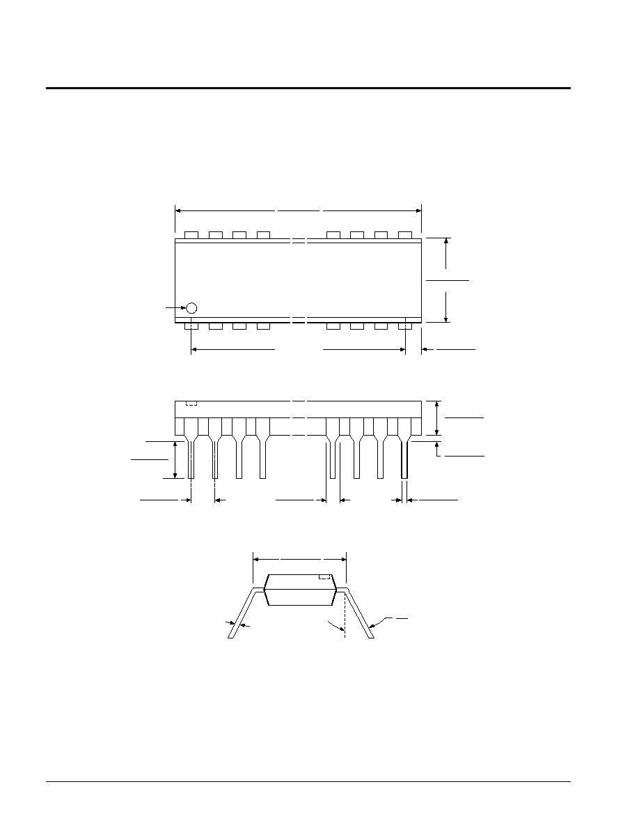
PACKAGING INFORMATION
3926 FHD F03
NOTE:
1. ALL DIMENSIONS IN INCHES (IN PARENTHESES IN MILLIMETERS)
2. PACKAGE DIMENSIONS EXCLUDE MOLDING FLASH
0.022 (0.56)
0.014 (0.36)
0.150 (3.81)
0.125 (3.18)
0.625 (15.87)
0.600 (15.24)
0.110 (2.79)
0.090 (2.29)
1.265 (32.13)
1.230 (31.24)
1.100 (27.94)
REF.
PIN 1 INDEX
0.162 (4.11)
0.140 (3.56)
0.030 (0.76)
0.015 (0.38)
PIN 1
SEATING
PLANE
0.065 (1.65)
0.040 (1.02)
0.557 (14.15)
0.530 (13.46)
0.080 (2.03)
0.065 (1.65)
0
∞
15
∞
24-LEAD PLASTIC DUAL IN-LINE PACKAGE TYPE P
TYP. 0.010 (0.25)
X88C64
13
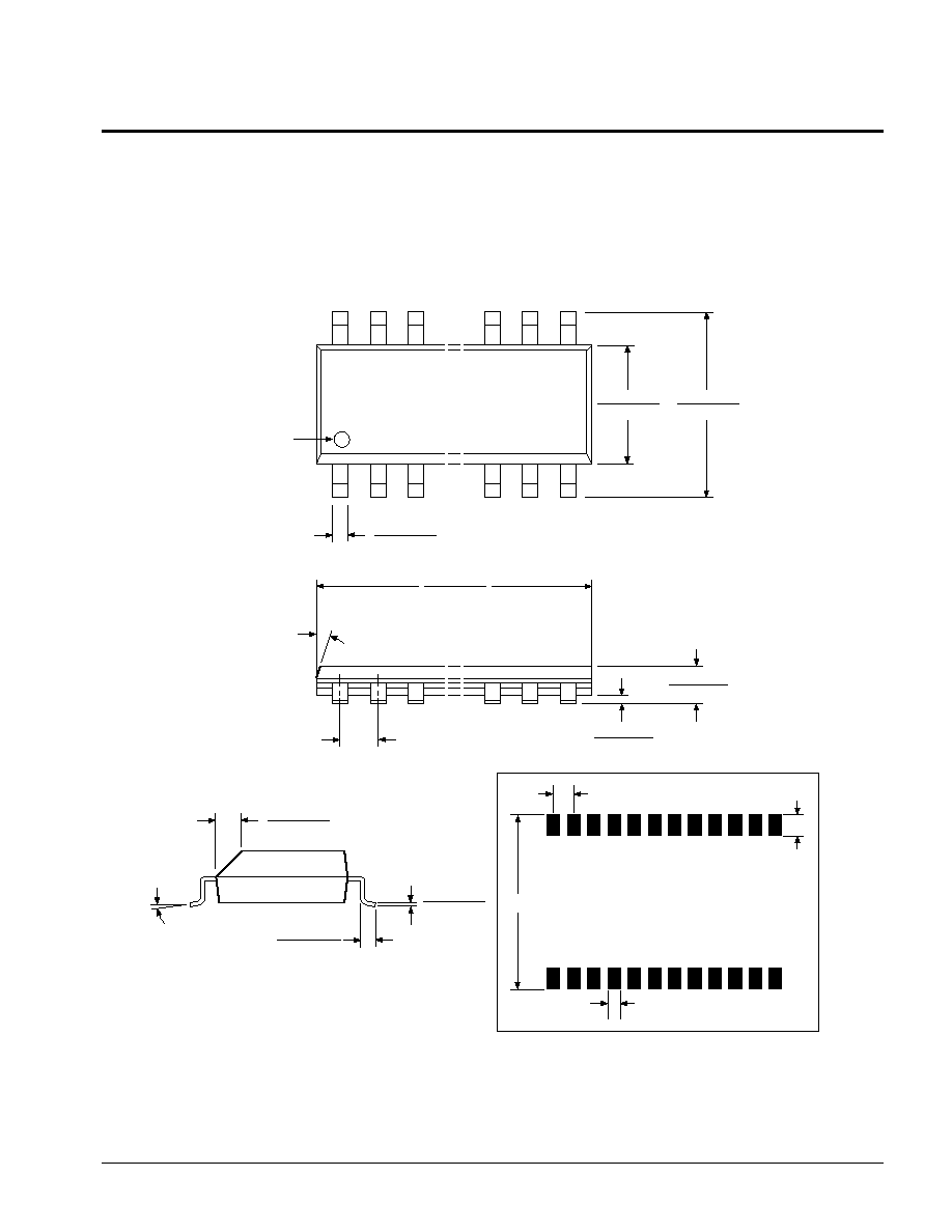
PACKAGING INFORMATION
0.290 (7.37)
0.299 (7.60)
0.393 (10.00)
0.420 (10.65)
0.014 (0.35)
0.020 (0.50)
PIN 1
PIN 1 INDEX
0.010 (0.25)
0.020 (0.50)
0.050 (1.27)
0.598 (15.20)
0.610 (15.49)
0.003 (0.10)
0.012 (0.30)
0.092 (2.35)
0.105 (2.65)
(4X) 7
∞
0.015 (0.40)
0.050 (1.27)
0.009 (0.22)
0.013 (0.33)
0
∞
≠ 8
∞
X 45
∞
3926 FHD F24
24-LEAD PLASTIC SMALL OUTLINE GULL WING PACKAGE TYPE S
NOTE: ALL DIMENSIONS IN INCHES (IN PARENTHESES IN MILLIMETERS)
0.420"
0.050" TYPICAL
0.050"
TYPICAL
0.030" TYPICAL
24 PLACES
FOOTPRINT

X88C64
14
ORDERING INFORMATION
LIMITED WARRANTY
Devices sold by Xicor, Inc. are covered by the warranty and patent indemnification provisions appearing in its Terms of Sale only. Xicor, Inc. makes
no warranty, express, statutory, implied, or by description regarding the information set forth herein or regarding the freedom of the described
devices from patent infringement. Xicor, Inc. makes no warranty of merchantability or fitness tor any purpose. Xicor, Inc. reserves the right to
discontinue production and change specifications and prices at any time and without notice.
Xicor, Inc. assumes no responsibility for the use of any circuitry other than circuitry embodied in a Xicor, Inc. product. No other circuits, patents,
licenses are implied.
US. PATENTS
Xicor products are covered by one or more of the following U.S. Patents: 4,263,664; 4,274,012; 4,300,212; 4,314,265; 4,326,134; 4,393,481;
4,404,475; 4,450,402; 4,486,769; 4,488,060; 4,520,461; 4,533,846; 4,599,706; 4,617,652; 4,668,932; 4,752,912; 4,829,482; 4,874,967; 4,883,976;
4,980,859; 5,012,132; 5,003,197; 5,023,694. Foreign patents and additional patents pending.
LIFE RELATED POLICY
In situations where semiconductor component failure may endanger life, system designers using this product should design the system with
appropriate error detection and correction, redundancy and back-up features to prevent such an occurrence.
Xicor's products are not authorized for use as critical components in life support devices or systems.
1. Life support devices or systems are devices or systems which, (a) are intended for surgical implant into the body, or (b) support or sustain life,
and whose failure to perform, when properly used in accordance with instructions for use provided in the labeling, can be reasonably expected
to result in a significant injury to the user.
2. A critical component is any component of a life support device or system whose failure to perform can be reasonably expected to cause the failure
of the life support device or system, or to affect its satety or effectiveness.
Device
Temperature Range
Blank = Commercial = 0
∞
C to +70
∞
C
I = Industrial = ≠40
∞
C to +85
∞
C
M = Military = ≠55
∞
C to +125
∞
C
MB = MIL-STD-883
Package
P = 24-Lead Plastic DIP
S = 24-Lead SOIC
X88C64 X X