 | –≠–ª–µ–∫—Ç—Ä–æ–Ω–Ω—ã–π –∫–æ–º–ø–æ–Ω–µ–Ω—Ç: X90100M8I | –°–∫–∞—á–∞—Ç—å:  PDF PDF  ZIP ZIP |

REV 1.4.7 9/8/03
1 of 10
www.xicor.com
NV Electronically Programmable Capacitor
X90100
FEATURES
∑ Non-volatile EEPROM storage of programmed
trim codes
∑ Power On Recall of capacitance setting
∑ High-Performance Electronically Trimmable
Capacitance
∑ Excellent Linearity: <0.5 LSB error
∑ Very Simple Digital Interface
∑ Fast Adjustments: 5µs max incremental change
∑ Eliminates the need for mechanical tuning
∑ Capacitance trimmable from 7.5 pF to 14.5 pF
(single-ended mode)
∑ Packages:
--MSOP (1.1mm x 3.0mm x 3.0mm)
--FCP (1.35mm x 1.32mm x 0.50mm)
APPLICATIONS
∑ Post-trim of low-cost regenerative receivers
∑ Tunable RF stages
∑ Low-cost, Low temperature drift oscillators
∑ Garage door openers
∑ Keyless entry
∑ Industrial wireless control
∑ Capacitive sensor trimming
∑ RFID tags
DESCRIPTION
The Xicor X90100 is a non-volatile electronically pro-
grammable capacitor. The device is programmed
through a simple digital interface. After programming,
the chosen setting for the device is retained by inter-
nal EEPROM storage whether or not DC power is
maintained. There are 32 programmable capacitance
values selectable, ranging from 7.5 pF to 14.5 pF in
0.23 pF increments, in single-ended mode. The dielec-
tric is highly stable, and the capacitance exhibits a very
low voltage coefficient. It has virtually no dielectric
absorbtion and has a very low temperature drift coeffi-
cient in differential mode (<50ppm/∞C).
The X90100 is programmed through three digital inter-
face pins, which have Schmitt triggers and pullup
resistors to secure code retention. The three pins,
INC, U/D, and CS, are identical in operation to other
Xicor chips with up/down interface, such as the x9315
5-bit Digitally Controlled Potentiometer (DCP).
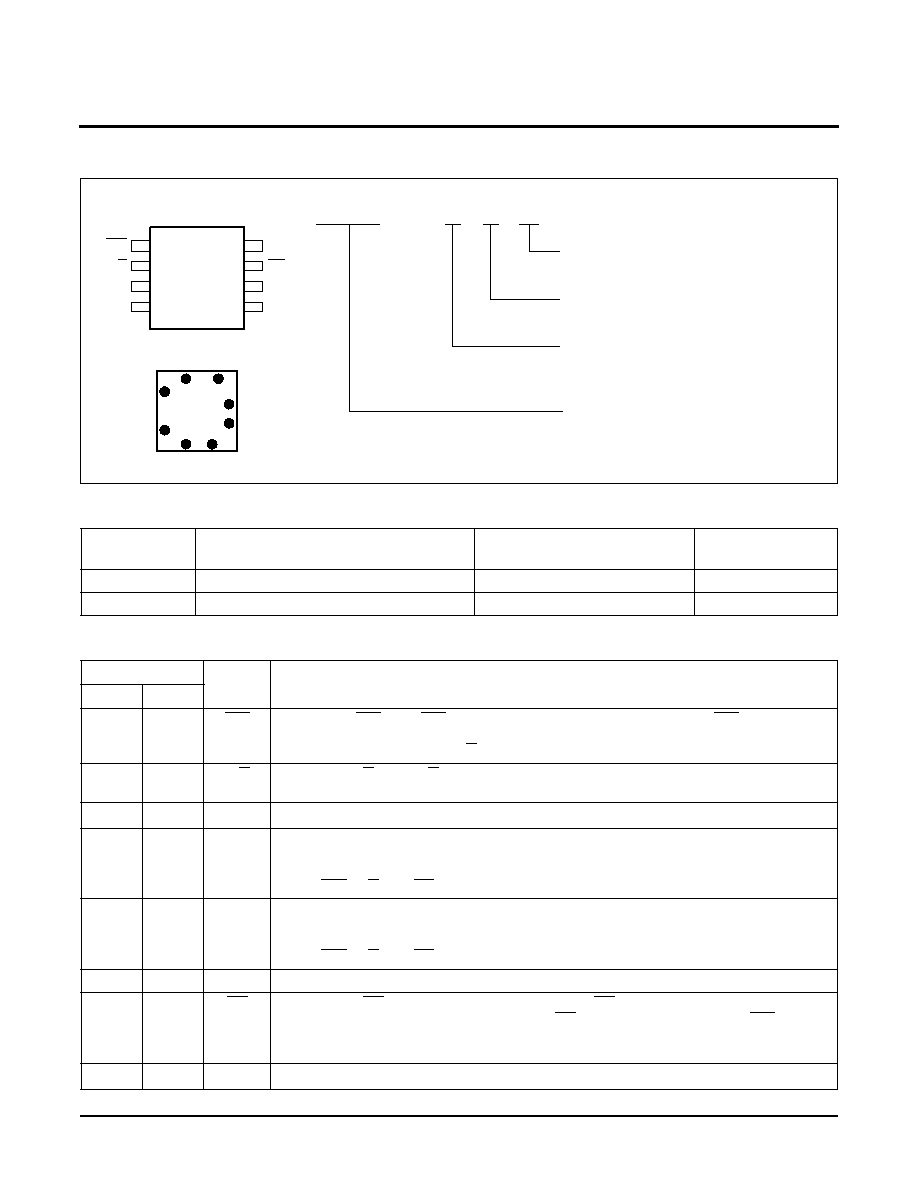
BLOCK DIAGRAM
Cm
C
PAD
U/D
INC
CS
V
SS
C
PAD
Cp
1*C
U
2*C
U
4*C
U
8*C
U
16*C
U
Logic and E
2
Power On Reset
V
CC
Small Packages
MSOP
Flipchip
2 of 10
REV 1.4.7 9/8/03
www.xicor.com
X90100
PIN CONFIGURATION
X90100 ORDERING CODES
PIN DESCRIPTIONS
Ordering
Number
Ctotal
Package
Temperature
Range
X90100M8I
7.5pF to 14.5pF, Single Ended
8-lead MSOP
-40C to +85C
X90100X8I
7.5pF to 14.5pF, Single Ended
8-lead FCP
-40C to +85C
Pin Number
Symbol
Brief Description
MSOP
FCP
1
6
INC
Increment (INC)
. The INC input is negative-edge triggered. Toggling INC will move the
capacitance value and either increment or decrement the counter in the direction indicat-
ed by the logic level on the U/D input.
2
7
U/D
Up/Down (U/D)
. The U/D input controls the direction of the trimmed capacitor value and
whether the counter is incremented or decremented.
3
8
V
SS
Ground
.
4
5
Cp
Cp
. The high (Cp) and low (Cm) terminals of the X90100 are equivalent to the fixed ter-
minals of a mechanical trimmable capacitor. The minimum dc voltage is V
SS
and the
maximum is V
CC
. The value of capacitance across the terminals is determined by digital
inputs INC, U/D, and CS.
5
4
Cm
Cm
. The high (Cp) and low (Cm) terminals of the X90100 are equivalent to the fixed ter-
minals of a mechanical trimmable capacitor. The minimum dc voltage is V
SS
and the
maximum is V
CC
. The value of capacitance across the terminals is determined by digital
inputs INC, U/D, and CS.
6
2
N/C
Not Connected
. Must be floating.
7
1
CS
Chip Select (CS)
. The device is selected when the CS input is LOW. The current counter
value is stored in nonvolatile memory when CS is returned HIGH while the INC input is
also HIGH. After the store operation is complete the X90100 will be placed in the low
power standby mode until the device is selected once again.
8
3
V
CC
Positive Supply Voltage
.
V
CC
CS
INC
U/D
1
2
3
4
8
7
6
5
X90100
MSOP
N/C
Cm
Vss
Cp
V
CC
Limits
Blank =2.7V to 5.5V
Temperature Range
I = Industrial = ≠40
∞C to +85∞C
Package
M = 8-Lead MSOP
X = 8-Bump FCP (Flipchip)
Base Part Number
X90100
X
X
X
1 2
3
4
6
5
7
8
X90100
FCP

3 of 10
REV 1.4.7 9/8/03
www.xicor.com
X90100
ABSOLUTE MAXIMUM RATINGS
Temperature under bias ....................≠65
∞
C to +135
∞
C
Storage temperature .........................≠65∞C to +150∞C
Voltage on CS, INC, U/D, C
P
, and
C
M
with respect to V
SS
........................... ≠1V to +7V
V = |V
CP
≠V
CM
| ..................................................... 5V
Lead temperature (soldering 10 seconds)..........300∞C
COMMENT
Stresses above those listed under "Absolute Maximum
Ratings" may cause permanent damage to the device.
This is a stress rating only; the functional operation of
the device (at these or any other conditions above
those listed in the operational sections of this specifi-
cation) is not implied. Exposure to absolute maximum
rating conditions for extended periods may affect
device reliability.
CAPACITOR CHARACTERISTICS
(Vcc=+5V, T
A
=25∞C, single ended mode, C
M
= 0V, unless otherwise stated.)
Notes:
(1) Absolute linearity is used to determine actual capacitance versus expected capacitance = C
(n)
(actual) -- C
(n)
(expected) = ±0.15 Ml.
(2) Relative linearity is a measure of the error in step size between settings = C
(n+1)
--[C
(n)
+ Ml] = ±0.15 Ml.
(3) lsb = least significant bit = C
TOT
/31.
(4) Typical values are for T
A
= 25∞C and nominal supply voltage.
(5) This parameter is not 100% tested
Symbol
Parameter
Limits
Test Conditions/Notes
Min.
Typ
(4)
.
Max.
Unit
Absolute accuracy
±15
%
V
Cp
C
p
terminal voltage
0
V
CC
V
V
Cm
C
m
terminal voltage
0
V
CC
V
C
Capacitance increments
0.23
pF
C
Capacitance range
7
pF
C
TOTAL
Capacitance at Code=0
7.5
pF
C
TOTAL
Capacitance at Code=31
14.5
pF
Q
Quality factor
(5)
7
f=315 MHz
Resolution
5
bits
INL
Absolute linearity error
(1)
±0.15
lsb
DNL
Relative linearity error
(2)
±0.15
lsb
TC
1
C
TOTAL
Temperature Coefficient
(5)
±50
ppm/∞C Differential Mode
V
CC
Supply Voltage
2.7
5.5
V

X90100
4 of 10
REV 1.4.7 9/8/03
www.xicor.com
D.C. OPERATING CHARACTERISTICS
(V
CC
= 5V, T
A
= 25∞C unless otherwise specified)
ENDURANCE AND DATA RETENTION
(V
CC
= 5V, T
A
= 25∞C unless otherwise specified)
Symbol
Parameter
Limits
Unit
Test Conditions
Min.
Typ.
(4)
Max.
I
CC1
V
CC
active current (Increment)
50
100
µA
CS = V
IL
, U/D = V
IL
or V
IH
and
INC = 0.4V @ max. t
CYC
I
CC2
V
CC
active current (Store) (EE-
PROM Store)
250
500
µA
CS = V
IH
, U/D = V
IL
or V
IH
and
INC = V
IH
@ max. t
WR
I
SB
Standby supply current
0.5
2
µA
CS = V
CC
≠ 0.3V, U/D and
INC = V
SS
or V
CC
≠ 0.3V
I
LI
CS, INC, U/D input leakage
current
-15
µA
V
IN
= V
SS
V
IH
CS, INC, U/D input HIGH voltage
V
CC
x 0.7
V
CC
+ 0.5
V
V
IL
CS, INC, U/D input LOW voltage
≠0.5
V
CC
x 0.1
V
C
IN
(5)
CS, INC, U/D input capacitance
10
pF
V
CC
= 5V, V
IN
= V
SS
,
T
A
= 25∞C, f = 1MHz
Parameter
Min.
Unit
Minimum endurance
100,000
Data changes per bit
Data retention
100
Years
A.C. CONDITIONS OF TEST
Input pulse levels
0V to 3V
Input rise and fall times
10ns
Input reference levels
1.5V

5 of 10
REV 1.4.7 9/8/03
www.xicor.com
X90100
A.C. OPERATING CHARACTERISTICS (V
CC
= 5V, T
A
= 25∞C unless otherwise specified)
A.C. TIMING
Notes: (6) MI in the A.C. timing diagram refers to the minimum incremental change in the C
TOTAL
output due to a change in the counter value.
(7) t
IH
+ t
IL
4µs
Symbol
Parameter
Limits
Unit
Min.
Typ.
(4)
Max.
t
Cl
CS to INC setup
100
ns
t
lD
INC HIGH to U/D change
100
ns
t
DI
U/D to INC setup
100
ns
t
lL
(7)
INC LOW period
1
µs
t
lH
(7)
INC HIGH period
1
µs
t
lC
INC Inactive to CS inactive
1
µs
t
CPHNS
(5)
CS Deselect time (NO STORE)
1
µs
t
CPHS
(5)
CS Deselect time (STORE)
10
ms
t
IW
INC to C
TOTAL
change
1
5
µs
t
CYC
INC cycle time
4
µs
t
R,
t
F
(5)
INC input rise and fall time
500
µs
t
PU
(5)
Power up to capacitance stable
5
µs
t
R
V
CC
(5)
V
CC
power-up rate
0.2
50
V/ms
t
WR
(5)
Store cycle
5
10
ms
CS
INC
U/D
C
TOTAL
t
CI
t
IL
t
IH
t
CYC
t
ID
t
IW
MI
(6)
t
IC
t
CPHS
t
F
t
R
10%
90%
90%
(Store)
t
DI
t
CPHNS

6 of 10
REV 1.4.7 9/8/03
www.xicor.com
X90100
POWER UP TIMING (DIGITAL INPUTS FLOATING, INTERNAL PULLUP ACTION SHOWN)
POWER UP AND DOWN REQUIREMENTS
There are no restrictions on the power-up or power-down conditions of V
CC
and the voltages applied to the Cp, Cm
pins provided that V
CC
is always more positive than or equal to V
Cp
, V
Cm
, i.e., V
CC
V
Cp
, V
Cm
. The V
CC
ramp rate
spec is always in effect.
Powerup Requirements
In order to prevent unwanted tap position changes or an inadvertant store, bring the CS and INC high before or
concurrently with the V
CC
pin. The logic inputs have internal active pullups to provide reliable powerup operation.
See powerup timing diagram.
V
CC
CS
INC
U/D
V
CC
= 3.3 or 5.0V
t
R
V
CC

7 of 10
REV 1.4.7 9/8/03
www.xicor.com
X90100
PIN CONFIGURATION
DETAILED PIN DESCRIPTIONS
Cp and Cm
The high (Cp) and low (Cm) terminals of the X90100
are equivalent to the fixed terminals of a mechanical
trimmable capacitor. The minimum dc voltage is V
SS
and the maximum is V
CC
. The value of capacitance
across the terminals is determined by digital inputs
INC, U/D, and CS.
Up/Down (U/D)
The U/D input controls the direction of the trimmed
capacitor value and whether the counter is incre-
mented or decremented. This pin has an active current
source pullup.
Increment (INC)
The INC input is negative-edge triggered. Toggling INC
will move the capacitance value and either increment
or decrement the counter in the direction indicated by
the logic level on the U/D input. This pin has an active
current source pullup.
Chip Select (CS)
The device is selected when the CS input is LOW. The
current counter value is stored in nonvolatile memory
when CS is returned HIGH while the INC input is also
HIGH. After the store operation is complete the
X90100 will be placed in the low power standby mode
until the device is selected once again. This pin has
active circuit source pullup.
N/C - This pin should be left floating.
PIN NAMES
PRINCIPLES OF OPERATION
There are three sections of the X90100: the input con-
trol, counter and decode section; the nonvolatile mem-
ory; and the capacitor array. The input control section
operates just like an up/down counter. The output of
this counter is decoded to turn on electronic switches
connecting internal units to the sum capacitor. Under
the proper conditions the contents of the counter can
be stored in nonvolatile memory and retained for future
use. The capacitor array is comprised of 31 individual
capacitors connected in parallel. At one end of each
element is an electronic switch that connects it to the
sum.
The capacitor, when at either end of the range, acts
like its mechanical equivalent and does not move
beyond the last position. That is, the counter does not
wrap around when clocked to either extreme.
The electronic switches on the device operate in a
"make before break" mode when the counter changes
positions. If the counter is moved several positions,
multiple units are connected to the total for t
IW
(INC to
C
TOTAL
change). The C
TOTAL
value for the device can
temporarily be increased by a significant amount if the
counter is moved several positions.
V
CC
CS
INC
U/D
1
2
3
4
8
7
6
5
X90100
MSOP
N/C (leave floating)
Cm
Vss
Cp
Symbol
Default
Description
Cp
output
Positive capacitor terminal
Cm
output
Negative capacitor terminal
V
SS
supply
Ground
V
CC
supply
Positive supply voltage
U/D
pull up
Up/Down control input
INC
pull up
Increment control input
CS
pull up
Chip Select control input

X90100
8 of 10
REV 1.4.7 9/8/03
www.xicor.com
When the device is powered-down, the last counter
position stored will be maintained in the nonvolatile
memory. When power is restored, the contents of the
memory are recalled and the capacitor is set to the
value last stored.
INSTRUCTIONS AND PROGRAMMING
The INC, U/D and CS inputs control the movement of
the capacitor total value. With CS set LOW the device
is selected and enabled to respond to the U/D and INC
inputs. HIGH to LOW transitions on INC will increment
or decrement (depending on the state of the U/D input)
a five bit counter. The output of this counter is decoded
to select one of thirty two capacitor combinations for
the capacitor array.
The value of the counter is stored in nonvolatile mem-
ory whenever CS transitions HIGH while the INC input
is also HIGH.
The system may select the X90100, move the capaci-
tor value and deselect the device without having to
store the latest count total in nonvolatile memory. After
the count movement is performed as described above
and once the new position is reached, the system must
keep INC LOW while taking CS HIGH. The new C
TO-
TAL
value will be maintained until changed by the sys-
tem or until a power-up/down cycle recalled the
previously stored data.
This procedure allows the system to always power-up
to a preset value stored in nonvolatile memory; then
during system operation minor adjustments can be
made. The adjustments might be based on user prefer-
ence, system parameter changes due to temperature
drift, etc.
The state of U/D may be changed while CS remains
LOW. This allows the host system to enable the device
and then move the counter up and down until the
proper trim is attained.
MODE SELECTION
CS
INC
U/D
Mode
L
H
Cap value Up
L
L
Cap value Down
H
X
Store Cap Position
H
X
X
Standby Current
L
X
No Store, Return to Standby
L
H
Cap value Up
(not recommended)
L
L
Cap value Down
(not recommended)
TABLE OF VALUES
Single-Ended Mode
Differential Mode
C
OUT
=
Code
31
∑ 7.0 + 7.5 (pF)
0
Code 31
C
OUT
= Code ∑ 0.35 + 1.00 (pF)
0
Code 31
C
p
C
m
X90100
X1
X2
Oscillator
Circuit
C
p
C
m
X90100
Oscillator
Circuit
C
p
C
s
Example of a single-ended circuit
Example of a differential mode circuit

9 of 10
REV 1.4.7 9/8/03
www.xicor.com
X90100
PACKAGING INFORMATION
8 Bump FCP Package
Note:
Coordinate (0,0) is at package center
Symbol
Min
Nominal
Max
Millimeters
Package Width
a
1.322
1.352
1.382
Package Length
b
1.297
1.327
1.357
Package Height
c
0.466
0.506
0.546
Body Thickness
d
0.381
0.406
0.431
Ball Height
e
0.085
0.100
0.115
Ball Diameter
f
0.100
0.125
0.140
Bump Name
X coordinate, µm
Y coordinate, µm
1
CS
28.4
478.8
2
NC/Test
352.9
471.8
3
V
CC
-488.6
351.3
4
Cm
491.9
210.8
5
Cp
491.9
-218.2
6
INC
-491.6
-382.7
7
U/D
-40.1
-479.2
8
V
SS
373.4
-488.7
a
b
c
d
f
e
e
Bottom View (Bumped Side)
Side View
Side View
1 2
3
4
6
5
7
8
AGC
YWW

Characteristics subject to change without notice.
10 of 10
LIMITED WARRANTY
Devices sold by Xicor, Inc. are covered by the warranty and patent indemnification provisions appearing in its Terms of Sale only. Xicor, Inc. makes no warranty,
express, statutory, implied, or by description regarding the information set forth herein or regarding the freedom of the described devices from patent infringement.
Xicor, Inc. makes no warranty of merchantability or fitness for any purpose. Xicor, Inc. reserves the right to discontinue production and change specifications and prices
at any time and without notice.
Xicor, Inc. assumes no responsibility for the use of any circuitry other than circuitry embodied in a Xicor, Inc. product. No other circuits, patents, or licenses are implied.
TRADEMARK DISCLAIMER:
Xicor and the Xicor logo are registered trademarks of Xicor, Inc. AutoStore, Direct Write, Block Lock, SerialFlash, MPS, BiasLock and XDCP are also trademarks of
Xicor, Inc. All others belong to their respective owners.
U.S. PATENTS
Xicor products are covered by one or more of the following U.S. Patents: 4,326,134; 4,393,481; 4,404,475; 4,450,402; 4,486,769; 4,488,060; 4,520,461; 4,533,846;
4,599,706; 4,617,652; 4,668,932; 4,752,912; 4,829,482; 4,874,967; 4,883,976; 4,980,859; 5,012,132; 5,003,197; 5,023,694; 5,084,667; 5,153,880; 5,153,691;
5,161,137; 5,219,774; 5,270,927; 5,324,676; 5,434,396; 5,544,103; 5,587,573; 5,835,409; 5,977,585. Foreign patents and additional patents pending.
LIFE RELATED POLICY
In situations where semiconductor component failure may endanger life, system designers using this product should design the system with appropriate error detection
and correction, redundancy and back-up features to prevent such an occurrence.
Xicor's products are not authorized for use in critical components in life support devices or systems.
1. Life support devices or systems are devices or systems which, (a) are intended for surgical implant into the body, or (b) support or sustain life, and whose failure to
perform, when properly used in accordance with instructions for use provided in the labeling, can be reasonably expected to result in a significant injury to the user.
2. A critical component is any component of a life support device or system whose failure to perform can be reasonably expected to cause the failure of the life
support device or system, or to affect its safety or effectiveness.
©Xicor, Inc. 2003 Patents Pending
REV 1.4.7 9/8/03
www.xicor.com
X90100
PACKAGING INFORMATION
0.118 ± 0.002
(3.00 ± 0.05)
0.040 ± 0.002
(1.02 ± 0.05)
0.150 (3.81)
Ref.
0.193 (4.90)
0.030 (0.76)
0.036 (0.91)
0.032 (0.81)
0.007 (0.18)
0.005 (0.13)
0.008 (0.20)
0.004 (0.10)
0.0216 (0.55)
7∞ Typ.
R 0.014 (0.36)
0.118 ± 0.002
(3.00 ± 0.05)
0.012 + 0.006 / -0.002
(0.30 + 0.15 / -0.05)
0.0256 (0.65) Typ.
8-Lead Miniature Small Outline Gull Wing Package Type M
NOTE:
1. ALL DIMENSIONS IN INCHES AND (MILLIMETERS)
0.220"
0.0256" Typical
0.025"
Typical
0.020"
Typical
8 Places
FOOTPRINT
Ref.