 | –≠–ª–µ–∫—Ç—Ä–æ–Ω–Ω—ã–π –∫–æ–º–ø–æ–Ω–µ–Ω—Ç: X9119 | –°–∫–∞—á–∞—Ç—å:  PDF PDF  ZIP ZIP |

REV 1.1.11 3/12/02
Characteristics subject to change without notice.
1 of 22
www.xicor.com
X9119
Single Digitally-Controlled (XDCP
TM
) Potentiometer
FEATURES
∑ 1024 Resistor Taps ≠ 10-Bit Resolution
∑ 2-Wire Serial Interface for write, read, and
transfer operations of the potentiometer
∑ Wiper Resistance, 40
Typical @ V
CC
= 5V
∑ Four Non-Volatile Data Registers
∑ Non-Volatile Storage of Multiple Wiper Positions
∑ Power On Recall. Loads Saved Wiper Position on
Power Up.
∑ Standby Current < 3µA Max
∑ V
CC
: 2.7V to 5.5V Operation
∑ 100K
End to End Resistance
∑ 100 yr. Data Retention
∑ Endurance: 100,000 Data Changes Per Bit Per
Register
∑ 14-Lead TSSOP, 15-Lead XBGA
∑ Low Power CMOS
∑ Single Supply version of the X9118
DESCRIPTION
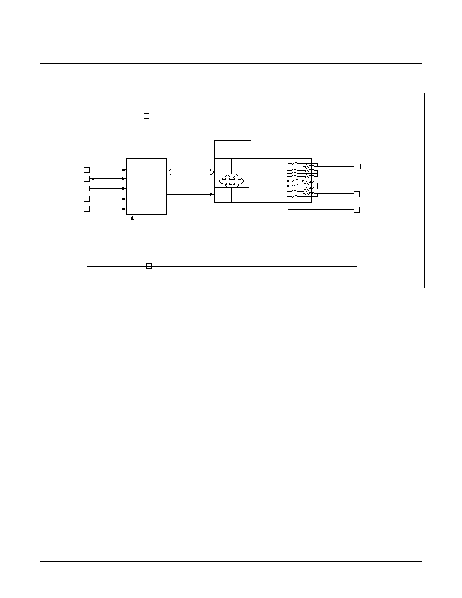
The X9119 integrates a single digitally controlled
potentiometer (XDCP) on a monolithic CMOS
integrated circuit.
The digital controlled potentiometer is implemented
using 1023 resistive elements in a series array.
Between each element are tap points connected to the
wiper terminal through switches. The position of the
wiper on the array is controlled by the user through the
2-wire bus interface. The potentiometer has associated
with it a volatile Wiper Counter Register (WCR) and a
four non-volatile Data Registers that can be directly
written to and read by the user. The contents of the
WCR controls the position of the wiper on the resistor
array though the switches. Powerup recalls the
contents of the default data register (DR0) to the WCR.
The XDCP can be used as a three-terminal
potentiometer or as a two terminal variable resistor in
a wide variety of applications including control,
parameter adjustments, and signal processing.
Single Supply / Low Power / 1024-tap / 2-Wire bus
A
PPLICATION
N
OTES
AND
D
EVELOPMENT
S
YSTEM
A V A I L A B L E
AN99 ∑ AN115 ∑ AN124 ∑AN133 ∑ AN134 ∑ AN135
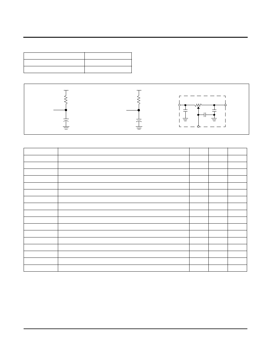
FUNCTIONAL DIAGRAM
R
H
R
L
Bus
R
W
Interface &
Control
POT
V
CC
V
SS
2-Wire
Bus
Address
Data
Status
Write
Read
Wiper
1024-taps
Transfer
NC
NC
100K
Power On Recall
Wiper Counter
Register (WCR)
Data Registers
(DR0-DR3)
Control
Interface
Preliminary Information
X9119
≠ Preliminary Information
Characteristics subject to change without notice.
2 of 22
REV 1.1.11 3/12/02
www.xicor.com
CIRCUIT LEVEL APPLICATIONS
∑ Vary the gain of a voltage amplifier
∑ Provide programmable dc reference voltages for
comparators and detectors
∑ Control the volume in audio circuits
∑ Trim out the offset voltage error in a voltage amplifier
circuit
∑ Set the output voltage of a voltage regulator
∑ Trim the resistance in Wheatstone bridge circuits
∑ Control the gain, characteristic frequency and
Q-factor in filter circuits
∑ Set the scale factor and zero point in sensor signal
conditioning circuits
∑ Vary the frequency and duty cycle of timer ICs
∑ Vary the dc biasing of a pin diode attenuator in RF
circuits
∑ Provide a control variable (I, V, or R) in feedback
circuits
SYSTEM LEVEL APPLICATIONS
∑ Adjust the contrast in LCD displays
∑ Control the power level of LED transmitters in
communication systems
∑ Set and regulate the DC biasing point in an RF
power amplifier in wireless systems
∑ Control the gain in audio and home entertainment
systems
∑ Provide the variable DC bias for tuners in RF
wireless systems
∑ Set the operating points in temperature control
systems
∑ Control the operating point for sensors in industrial
systems
∑ Trim offset and gain errors in artificial intelligent
systems
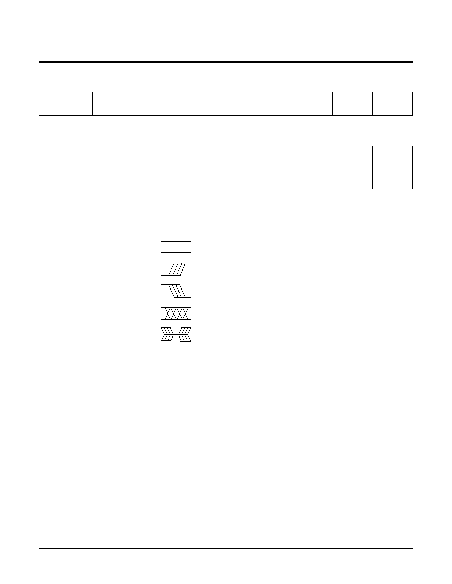
DETAILED FUNCTIONAL DIAGRAM
SCL
A1
SDA
A2
WP
Interface
and
Control
Circuitry
V
CC
V
SS
DR0
DR1
DR2 DR3
Wiper
Counter
Register
(WCR)
R
H
R
L
Data
R
W
1024-taps
100K
Control
Power On
Recall
A0
X9119
≠ Preliminary Information
Characteristics subject to change without notice.
3 of 22
REV 1.1.11 3/12/02
www.xicor.com
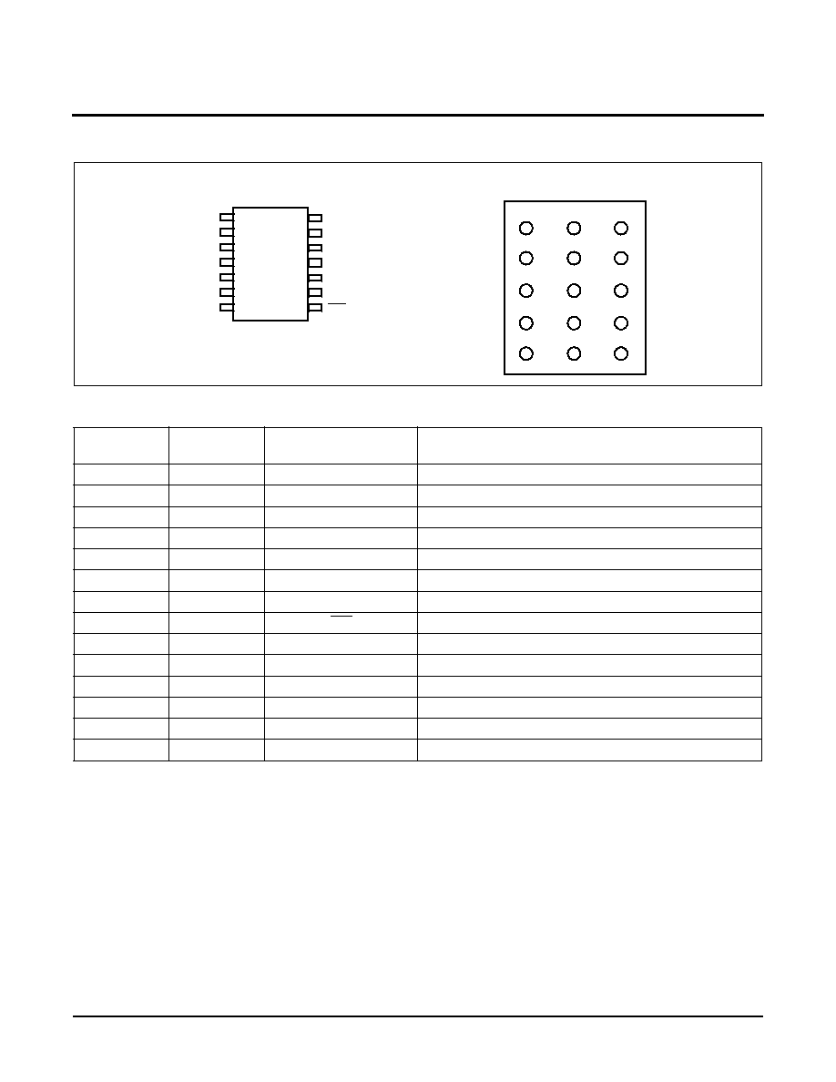
PIN CONFIGURATION
PIN ASSIGNMENTS
Pin
(TSSOP)
Pin
(XBGA) Symbol
Function
1
D1, A3
NC
No Connect
2
B3
A0
Device Address for 2-wire bus
3
B2
NC
No Connect
4
C3
A2
Device Address for 2-wire bus
5
D3
SCL
Serial Clock for 2-wire bus
6
E3
SDA
Serial Data Input/Output for 2-wire bus
7
E2
V
SS
System Ground
8
D2
WP
Hardware Write Protect
9
E1
A1
Device Address for 2-wire bus
10
C2
NC
No Connect
11
C1
R
W
Wiper terminal of the Potentiometer
12
B1
R
H
High terminal of the Potentiometer
13
A1
R
L
Low terminal of the Potentiometer
14
A2
V
CC
System Supply Voltage
V
CC
R
L
V
SS
1
2
3
4
5
6
7
8
14
13
12
11
10
9
NC
R
W
A2
A1
TSSOP
R
H
X9119
XBGA
A0
NC
SDA
NC
SCL
WP
X9119
A1
A2
A3
B1
B2
B3
C1
C2
C3
D1
D2
D3
E1
E2
E3
RL
V
CC
NC
RH
NC
A0
RW
NC
A2
NC
WPN
SCL
A1
V
SS
SDA

X9119 ≠ Preliminary Information
Characteristics subject to change without notice.
4 of 22
REV 1.1.11 3/12/02
www.xicor.com
PIN DESCRIPTIONS
Bus Interface Pins
S
ERIAL
D
ATA
I
NPUT
/O
UTPUT
(SDA)
The SDA is a bidirectional serial data input/output pin
for a 2-wire slave device and is used to transfer data
into and out of the device. It receives device address,
opcode, wiper register address and data sent from an
2-wire master at the rising edge of the serial clock
SCL, and it shifts out data after each falling edge of the
serial clock SCL.
It is an open drain output and may be wire-ORed with
any number of open drain or open collector outputs. An
open drain output requires the use of a pull-up resistor.
For selecting typical values, refer to the guidelines for
calculating typical values on the bus pull-up resistors
graph.
S
ERIAL
C
LOCK
(SCL)
This input is used by 2-wire master to supply 2-wire
serial clock to the X9119.
D
EVICE
A
DDRESS
(A
2
≠A
0
)
The Address inputs are used to set the least significant
3 bits of the 8-bit slave address. A match in the slave
address serial data stream must be made with the
Address input in order to initiate communication with
the X9119. A maximum of 8 devices may occupy the 2-
wire serial bus.
Hardware Write Protect Input (WP)
The WP pin when LOW prevents nonvolatile writes to
the Data Registers.
Potentiometer Pins
R
H
, R
L
The R
H
and R
L
pins are equivalent to the terminal
connections on a mechanical potentiometer.
R
W
The wiper pin are equivalent to the wiper terminal of a
mechanical potentiometer.
Bias Supply Pins
S
YSTEM
S
UPPLY
V
OLTAGE
(V
CC
)
AND
S
UPPLY
G
ROUND
(V
SS
)
The V
CC
pin is the system supply voltage. The V
SS
pin
is the system ground.
Other Pins
N
O
C
ONNECT
No connect pins should be left open. These pins are
used for Xicor manufacturing and testing purposes.
PRINCIPLES OF OPERATION
The X9119 is an integrated microcircuit incorporating a
resistor array and its associated registers and counters
and the serial interface logic providing direct
communication between the host and the digitally
controlled potentiometer. This section provides detail
description of the following:
≠ Resistor Array Description
≠ Serial Interface Description
≠ Instruction and Register Description
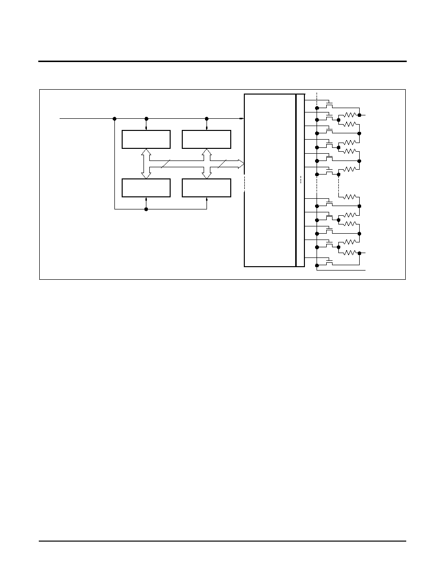
Resistor Array Description
The X9119 is comprised of a resistor array. The array
contains, in effect, 1023 discrete resistive segments
that are connected in series (see Figure 1). The
physical ends of each array are equivalent to the fixed
terminals of a mechanical potentiometer (R
H
and R
L
inputs).
At both ends of each array and between each resistor
segment is a CMOS switch connected to the wiper
(R
W
) output. Within each individual array only one
switch may be turned on at a time. These switches are
controlled by the Wiper Counter Register (WCR). The
10-bits of the WCR (WCR[9:0]) are decoded to select,
and enable, one of 1024 switches.
The WCR may be written directly. The Data Registers
and the WCR can be read and written by the host
system.
X9119 ≠ Preliminary Information
Characteristics subject to change without notice.
5 of 22
REV 1.1.11 3/12/02
www.xicor.com
Figure 1. Detailed Potentiometer Block Diagram
Serial Data Path
From Interface
Register 0
Serial
Bus
Input
Parallel
Bus
Input
Counter
Register
RH
RL
R
W
10
10
C
O
U
N
T
E
R
D
E
C
O
D
E
If WCR = 000[HEX] then R
W
= R
L
If
WCR = 3FF[HEX]
then
R
W
=
R
H
Wiper
(WCR)
(DR0)
Circuitry
Register 1
(DR1)
Register 2
(DR2)
Register 3
(DR3)
Serial Interface Description
S
ERIAL
I
NTERFACE
The X9119 supports a bidirectional bus oriented
protocol. The protocol defines any device that sends
data onto the bus as a transmitter and the receiving
device as the receiver. The device controlling the
transfer is a master and the device being controlled is
the slave. The master will always initiate data transfers
and provide the clock for both transmit and receive
operations. Therefore, the X9119 will be considered a
slave device in all applications.
C
LOCK
AND
D
ATA
C
ONVENTIONS
Data states on the SDA line can change only during
SCL LOW periods. SDA state changes during SCL
HIGH are reserved for indicating start and stop
conditions. See Figure 3.
S
TART
C
ONDITION
All commands to the X9119 are preceded by the start
condition, which is a HIGH to LOW transition of SDA
while SCL is HIGH. The X9119 continuously monitors
the SDA and SCL lines for the start condition and will
not respond to any command until this condition is met.
See Figure 3.
S
TOP
C
ONDITION
All communications must be terminated by a stop
condition, which is a LOW to HIGH transition of SDA
while SCL is HIGH. See Figure 3.
A
CKNOWLEDGE
Acknowledge is a software convention used to provide
a positive handshake between the master and slave
devices on the bus to indicate the successful receipt of
data. The transmitting device, either the master or the
slave, will release the SDA bus after transmitting eight
bits. The master generates a ninth clock cycle and
during this period the receiver pulls the SDA line LOW
to acknowledge that it successfully received the eight
bits of data.
The X9119 will respond with an acknowledge after
recognition of a start condition and its slave address
and once again after successful receipt of the
command byte. If the command is followed by a data
byte the X9119 will respond with a final acknowledge.
See Figure 2.

X9119 ≠ Preliminary Information
Characteristics subject to change without notice.
6 of 22
REV 1.1.11 3/12/02
www.xicor.com
Figure 2. Acknowledge Response from Receiver
SCL from
Master
Data Output
from Transmitter
1
8
9
START
ACKNOWLEDGE
Data Output
from Receiver
A
CKNOWLEDGE
P
OLLING
The disabling of the inputs, during the internal
nonvolatile write operation, can be used to take
advantage of the typical 5ms EEPROM write cycle
time. Once the stop condition is issued to indicate the
end of the nonvolatile write command the X9119
initiates the internal write cycle. ACK polling, Flow 1,
can be initiated immediately. This involves issuing the
start condition followed by the device slave address. If
the X9119 is still busy with the write operation no ACK
will be returned. If the X9119 has completed the write
operation an ACK will be returned and the master can
then proceed with the next operation.
FLOW 1. ACK Polling Sequence
Nonvolatile Write
Command Completed
EnterACK Polling
Issue
START
Issue Slave
Address
ACK
Returned?
Further
Operation?
Issue
Instruction
Issue STOP
No
Yes
Yes
Proceed
Issue STOP
No
Proceed
X9119 ≠ Preliminary Information
Characteristics subject to change without notice.
7 of 22
REV 1.1.11 3/12/02
www.xicor.com
Instruction and Register Description
D
EVICE
A
DDRESSING
: I
DENTIFICATION
B
YTE
(ID
AND
A)
Following a start condition the master must output the
address of the slave it is accessing. The most
significant four bits of the slave address are the device
type identifier. The ID[3:0] bits is the device id for the
X9119; this is fixed as 0101[B] (refer to Table 1).
The A2≠A0 bits in the ID byte is the internal slave
address. The physical device address is defined by the
state of the A2≠A0 input pins. The slave address is
externally specified by the user. The X9119 compares
the serial data stream with the address input state; a
successful compare of both address bits is required for
the X9119 to successfully continue the command
sequence. Only the device which slave address
matches the incoming device address sent by the
master executes the instruction. The A2≠A0 inputs can
be actively driven by CMOS input signals or tied to V
CC
or V
SS
. The R/W bit is the LSB and is be used to
program the device for read or write operations.
I
NSTRUCTION
B
YTE
AND
R
EGISTER
S
ELECTION
The next byte sent to the X9119 contains the
instruction and register pointer information. The three
most significant bits are used provide the instruction
opcode (IOP[2:0]). The RB and RA bits point to one of
the four registers. The format is shown below in
Table 2.
Table 3 provides a complete summary of the
instruction set opcodes.
Table 1. Identification Byte Format
Table 2. Instruction Byte Format
Register Selected
RB
RA
DR0
0
0
DR1
0
1
DR2
1
0
DR3
1
1
ID3
ID2
ID1
ID0
A2
A1
A0
R/W
0
1
0
1
(MSB)
(LSB)
Device Type
Identifies
Internal Slave
Address
Read or
Write Bit
I2
I1
I0
0
RB
RA
0
0
(MSB)
(LSB)
Instruction
Opcode
Register
Selection
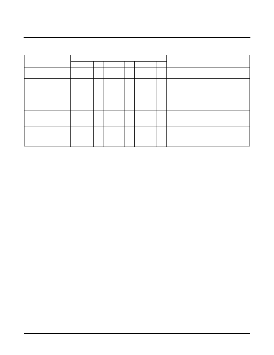
X9119 ≠ Preliminary Information
Characteristics subject to change without notice.
8 of 22
REV 1.1.11 3/12/02
www.xicor.com
Table 3. Instruction Set
Note:
(1) 1/o = data is one or zero.
Instruction
Instruction Set
Operation
R/W
I
2
I
1
I
0
0
RB
RA
0
0
Read Wiper Counter
Register
1
1
0
0
0
0
0
0
0
Read the contents of the Wiper Counter
Register
Write Wiper Counter
Register
0
1
0
1
0
0
0
0
0
Write new value to the Wiper Counter
Register
Read Data Register
1
1
0
1
0
1/0
1/0
0
0
Read the contents of the Data Register
pointed to RB-RA.
Write Data Register
0
1
1
0
0
1/0
1/0
0
0
Write new value to the Data Register
pointed to RB-RA.
XFR Data Register to
Wiper Counter Register
1
1
1
0
0
1/0
1/0
0
0
Transfer the contents of the Data Register
pointed to by RB-RA.to the Wiper Counter
Register
XFR Wiper Counter
Register to Data Regis-
ter
0
1
1
1
0
1/0
1/0
0
0
Transfer the contents of the Wiper Counter
Register to the Data Register pointed to by
RB-RA.
Instruction and Register Description
D
EVICE
A
DDRESSING
W
IPER
C
OUNTER
R
EGISTER
(WCR)
The X9119 contains a Wiper Counter Registers (see
Table 4) for the XDCP potentiometer. The WCR is
equivalent to a serial-in, parallel-out register/counter
with its outputs decoded to select one of 1024
switches along its resistor array. The contents of the
WCR can be altered in one of three ways: (1) it may be
written directly by the host via the write wiper counter
register instruction (serial load); (2) it may be written
indirectly by transferring the contents of one of four
associated data registers via the XFR data register; (3)
it is loaded with the contents of its data register zero
(R0) upon power-up.
The Wiper Counter Register is a volatile register; that
is, its contents are lost when the X9119 is powered-
down. Although the register is automatically loaded
with the value in DR0 upon power-up, this may be
different from the value present at power-down. Power-
up guidelines are recommended to ensure proper
loadings of the DR0 value into the WCR.
D
ATA
R
EGISTERS
(DR0
TO
DR3)
The potentiometer has four 10-bit non-volatile Data
Registers. These can be read or written directly by the
host. Data can also be transferred between any of the
four Data Registers and the Wiper Counter Register.
All operations changing data in one of the data
registers is a nonvolatile operation and will take a
maximum of 10ms.
If the application does not require storage of multiple
settings for the potentiometer, the Data Registers can
be used as regular memory locations for system
parameters or user preference data.
Bit 9≠Bit 0 are used to store one of the 1024 wiper
position (0 ~1023).

X9119
≠ Preliminary Information
Characteristics subject to change without notice.
9 of 22
REV 1.1.11 3/12/02
www.xicor.com
Table 4. Wiper Control Register, WCR (10-bit), WCR9≠WCR0: Used to store the current wiper position (Volatile, V)
Table 5. Data Register, DR (10-bit), Bit 9≠Bit 0: Used to store wiper positions or data (Non-Volatile, NV)
WCR9
WCR8
WCR7
WCR6
WCR5
WCR4
WCR3
WCR2
WCR1
WCR0
V
V
V
V
V
V
V
V
V
V
(MSB)
(LSB)
Bit 9
Bit 8
Bit 7
Bit 6
Bit 5
Bit 4
Bit 3
Bit 2
Bit 1
Bit 0
NV
NV
NV
NV
NV
NV
NV
NV
NV
NV
MSB
LSB
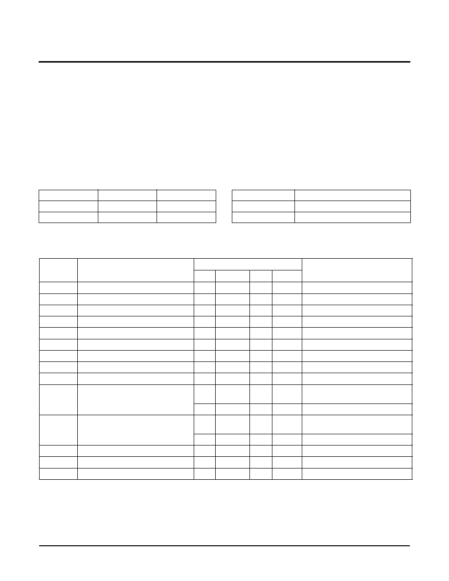
Four of the six instructions are four bytes in length.
These instructions are:
≠ Read Wiper Counter Register ≠ read the current
wiper position of the selected potentiometer,
≠ Write Wiper Counter Register ≠ change current
wiper position of the selected potentiometer,
≠ Read Data Register ≠ read the contents of the
selected Data Register;
≠ Write Data Register ≠ write a new value to the
selected Data Register.
The basic sequence of the four byte instructions is
illustrated in Figure 3. These four-byte instructions
exchange data between the WCR and one of the Data
Registers. A transfer from a data register to a WCR is
essentially a write to a static RAM, with the static RAM
controlling the wiper position. The response of the
wiper to this action will be delayed by t
WRL
. A transfer
from the WCR (current wiper position), to a data
register is a write to nonvolatile memory and takes a
minimum of t
WR
to complete. The transfer can occur
between one of the four potentiometers and one of its
associated registers.
Two instructions (see Figure 4) require a two-byte
sequence to complete. These instructions transfer data
between the host and the X9119; either between the
host and one of the data registers or directly between
the host and the Wiper Counter Register. These
instructions are:
≠ XFR Data Register to Wiper Counter Register ≠
This transfers the contents of one specified Data
Register to the Wiper Counter Register.
≠ XFR Wiper Counter Register to Data Register ≠
This transfers the contents of the Wiper Counter
Register to the specified Data Register.
See Instruction format for more details.
P
OWER
U
P
AND
D
OWN
R
EQUIREMENTS
There are no restrictions on the power-up condition of
Vcc and the voltages applied to the potentiometer pins
provided that the Vcc is always more positive than or
equal to the voltages at R
H
, R
L
, and R
W
, i.e. V
CC
R
H
,
R
L
, R
W
. There are no restrictions on the power-down
condition. However, the datasheet parameters for the
DCP do not apply until 1milisecond after V
CC
reaches
its final value.
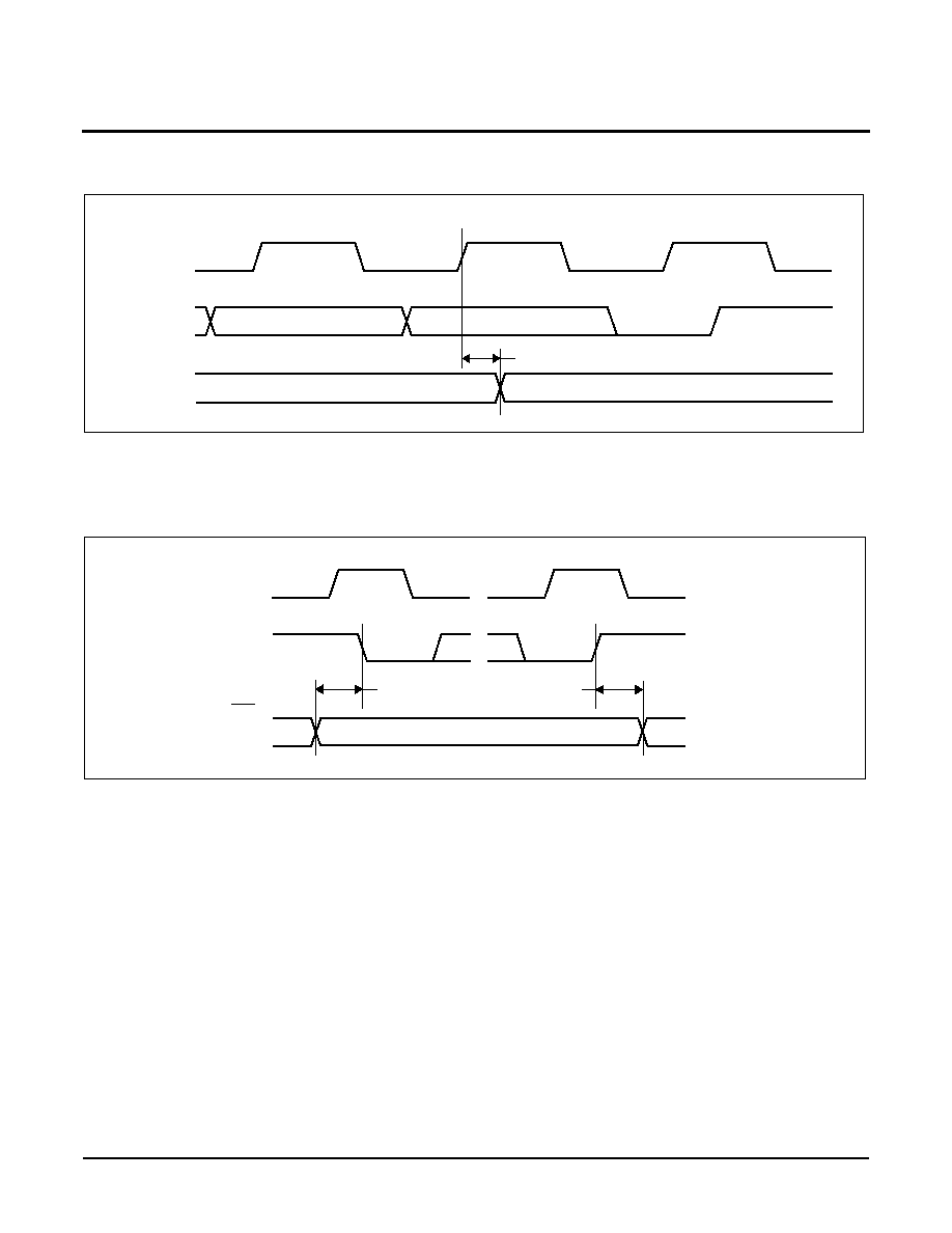
Figure 3. Two-Byte Instruction Sequence
S
T
A
R
T
0
1
0
1
A2
A1
A0 R/W
A
C
K
I2
I1
I0
0
RB RA 0
A
C
K
SCL
SDA
S
T
O
P
0
0
0
ID3 ID2 ID1 ID0
Device ID
Internal
Instruction
Opcode
Address
Register
Address

X9119
≠ Preliminary Information
Characteristics subject to change without notice.
10 of 22
REV 1.1.11 3/12/02
www.xicor.com
Figure 4. Four-Byte Instruction Sequence (Write or Read for WCR or Data Registers)
INSTRUCTION FORMAT
Read Wiper Counter Register (WCR)
Write Wiper Counter Register (WCR)
Read Data Register (DR)
S
T
A
R
T
Device Type
Identifier
Device
Addresses
S
A
C
K
Instruction
Opcode
Register
Addresses
S
A
C
K
Wiper Position
(Sent by Slave on SDA)
M
A
C
K
Wiper Position
(Sent by Slave on SDA)
M
A
C
K
S
T
O
P
0
1
0
1 A2 A1 A0
R / W
= 1
1
0
0
0
0
0
0
0
X
X
X
X
X
X
W
C
R
9
W
C
R
8
W
C
R
7
W
C
R
6
W
C
R
5
W
C
R
4
W
C
R
3
W
C
R
2
W
C
R
1
W
C
R
0
S
T
A
R
T
Device Type
Identifier
Device
Addresses
S
A
C
K
Instruction
Opcode
Register
Addresses
S
A
C
K
Wiper Position
(Sent by Master on SDA)
S
A
C
K
Wiper Position
(Sent by Master on SDA)
S
A
C
K
S
T
O
P
0
1
0
1 A2 A1 A0
R /
W
= 0
1
0
1
0
0
0
0
0
X
X
X
X
X
X
W
C
R
9
W
C
R
8
W
C
R
7
W
C
R
6
W
C
R
5
W
C
R
4
W
C
R
3
W
C
R
2
W
C
R
1
W
C
R
0
S
T
A
R
T
Device Type
Identifier
Device
Addresses
S
A
C
K
Instruction
Opcode
Register
Addresses
S
A
C
K
Wiper Position
(Sent by Slave on SDA)
M
A
C
K
wiper position or data
(Sent by Slave on SDA)
M
A
C
K
S
T
O
P
0
1
0
1 A2 A1 A0
R /
W
= 1
1
0
1
0 RB RA 0
0
X
X
X
X
X
X
W
C
R
9
W
C
R
8
W
C
R
7
W
C
R
6
W
C
R
5
W
C
R
4
W
C
R
3
W
C
R
2
W
C
R
1
W
C
R
0
S
T
A
R
T
A
C
K
A
C
K
SCL
SDA
A
C
K
S
T
O
P
A
C
K
ID3 ID2 ID1 ID0 A2 A1 A0 R/W
I2
0
0
0
X
X
0
0
X X
X
W
C
R
9
W
C
R
8
W
C
R
7
W
C
R
6
W
C
R
5
W
C
R
4
W
C
R
3
W
C
R
2
W
C
R
1
W
C
R
0
I1 I0
0 RB RA
0
1
0
1
X
X
X
Device ID
Internal
Address
Instruction
Opcode
Register
Address
Wiper or Data
Position
X9119 ≠ Preliminary Information
Characteristics subject to change without notice.
11 of 22
REV 1.1.11 3/12/02
www.xicor.com
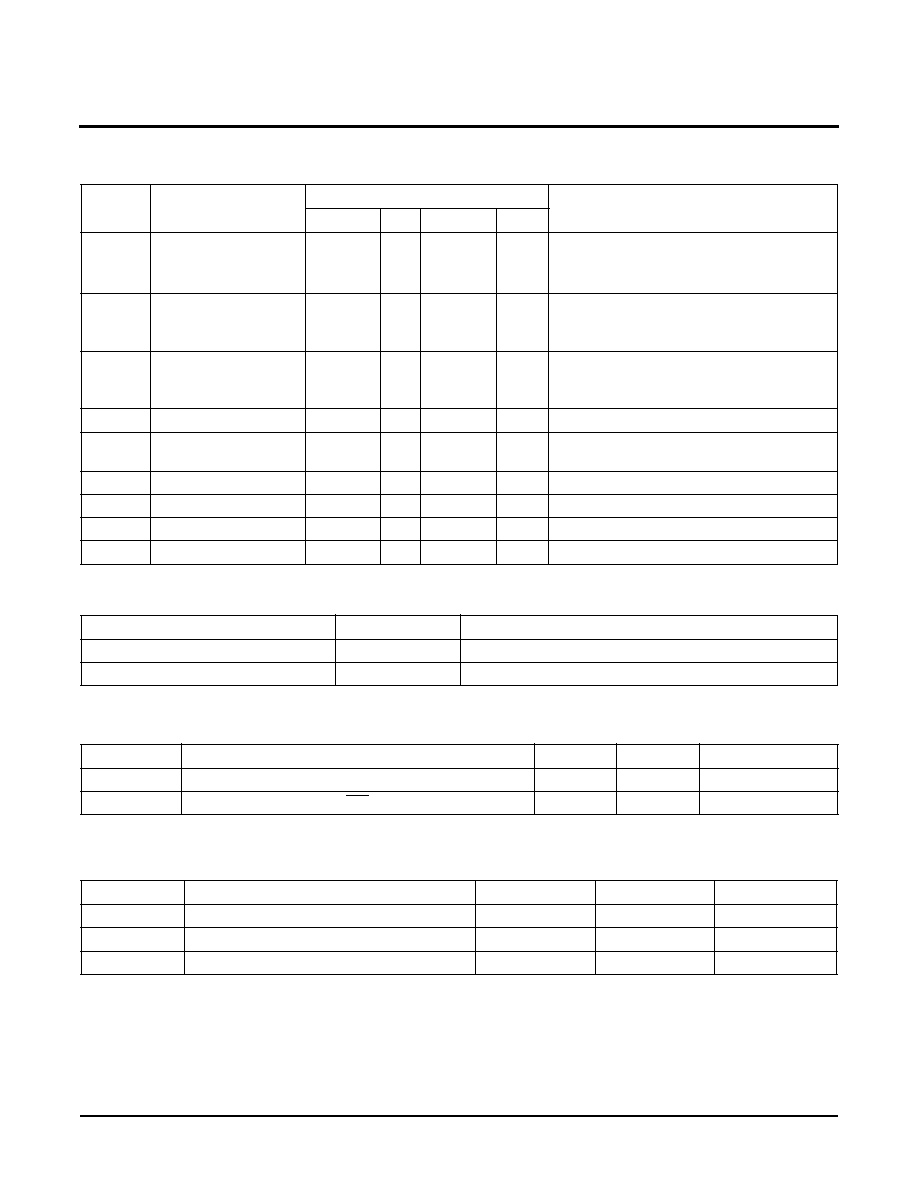
Write Data Register (DR)
Transfer Wiper Counter Register (WCR) to Data Register (DR)
Transfer Data Register (DR) to Wiper Counter Register (WCR)
Notes: (1) "A2 ~ A0": stand for the device addresses sent by the master.
(2) WCRx refers to wiper position data in the Wiper Counter Register
S
T
A
R
T
Device Type
Identifier
Device
Addresses
S
A
C
K
Instruction
Opcode
Register
Addresses
S
A
C
K
Wiper Position or Data
(Sent by Master on SDA)
S
A
C
K
Wiper Position or Data
(Sent by Master on SDA)
S
A
C
K
S
T
O
P
HIGH-V
OL
T
A
GE
WRITE CYCLE
0
1
0
1 A2 A1 A0
R /
W
= 0
1 1 0 0 RB RA 0
0
X X X X X X
W
C
R
9
W
C
R
8
W
C
R
7
W
C
R
6
W
C
R
5
W
C
R
4
W
C
R
3
W
C
R
2
W
C
R
1
W
C
R
0
S
T
A
R
T
Device Type
Identifier
Device
Addresses
S
A
C
K
Instruction
Opcode
Register
Addresses
S
A
C
K
S
T
O
P
HIGH-VOLTAGE
WRITE CYCLE
0
1
0
1
A2 A1 A0
R /
W
= 0
1
1
1
0 RB RA 0
0
S
T
A
R
T
Device Type
Identifier
Device
Addresses
S
A
C
K
Instruction
Opcode
Register
Addresses
S
A
C
K
S
T
O
P
0
1
0
1 A2 A1 A0
R /
W
= 1
1
1
0
0 RB RA 0
0
X9119
≠ Preliminary Information
Characteristics subject to change without notice.
12 of 22
REV 1.1.11 3/12/02
www.xicor.com
ABSOLUTE MAXIMUM RATINGS
Temperature under bias.................... ≠65∞C to +135∞C
Storage temperature......................... ≠65∞C to +150∞C
Voltage on SCL, SDA, or any address input
with respect to V
SS
................................. ≠1V to +7V
V = | (VH≠VL) | ......................................................5V
Lead temperature (soldering, 10 seconds) ........ 300
∞C
I
W
(10 seconds) ..................................................±6mA
COMMENT
Stresses above those listed under "Absolute Maximum
Ratings" may cause permanent damage to the device.
This is a stress rating only; the functional operation of
the device (at these or any other conditions above
those listed in the operational sections of this
specification) is not implied. Exposure to absolute
maximum rating conditions for extended periods may
affect device reliability.
ANALOG CHARACTERISTICS (Over recommended industrial (2.7V) operation conditions unless otherwise stated.)
Notes: (1) Absolute linearity is utilized to determine actual wiper voltage versus expected voltage as determined by wiper position when used
as a potentiometer.
(2) Relative linearity is utilized to determine the actual change in voltage between two successive tap positions when used as a
potentiometer. It is a measure of the error in step size.
(3) MI = RTOT / 1023 or (R
H
≠ R
L
) / 1023, single pot
(4) n = 0, 1, 2, ...,1023; m =0, 1, 2, ..., 1022.
(5) ESD Rating on RH, RL, RW pins is 1.5KV (HBM, 1.0µA leakage maximum), ESD rating on all other pins is 2.0kV.
Symbol
Parameter
Limits
Test Conditions
Min.
Typ.
Max.
Units
R
TOTAL
End to End Resistance
100
k
End to End Resistance Tolerance
±20
%
Power Rating
50
mW
25∞C, each pot
I
W
Wiper Current
±3
mA
R
W
Wiper Resistance
150
500
Wiper Current =
± 3mA, V
CC
= 3V
R
W
Wiper Resistance
40
100
I
W
=
± 3mA, V
CC
= 5V
V
TERM
Voltage on any R
H
or R
L
Pin
V
SS
5
V
V
SS
= 0V
Noise
-120
dBV
Ref: 1V
Resolution
0.1
%
Absolute Linearity
(1)
±1
MI
(3)
R
w(n)(actual)
≠ R
w(n)(expected)
,
where n=8 to 1006
±1.5
MI
(3)
R
w(n)(actual)
≠ R
w(n)(expected)
(5)
Relative Linearity
(2)
±0.5
MI
(3)
R
w(m + 1)
≠ [R
w(m)
+ MI], where
m=8 to 1006
±1
MI
(3)
R
w(m + 1)
≠ [R
w(m)
+ MI]
(5)
Temperature Coefficient of R
TOTAL
±300
ppm/∞C
Ratiometric Temp. Coefficient
20
ppm/∞C
C
H
/C
L
/C
W
Potentiometer Capacitancies
10/10/25
pF
See Macro model
RECOMMENDED OPERATING CONDITIONS
Temp
Min.
Max.
Commercial
0
∞C
+70
∞C
Industrial
≠40
∞C
+85
∞C
Device
Supply Voltage (V
CC
) Limits
(4)
X9119
5V
±10%
X9119-2.7
2.7V to 5.5V
X9119
≠ Preliminary Information
Characteristics subject to change without notice.
13 of 22
REV 1.1.11 3/12/02
www.xicor.com
D.C. OPERATING CHARACTERISTICS (Over the recommended operating conditions unless otherwise specified.)
ENDURANCE AND DATA RETENTION
CAPACITANCE
POWER-UP TIMING
Notes: (6) This parameter is not 100% tested.
(7) t
PUR
and t
PUW
are the delays required from the time the (last) power supply (Vcc-) is stable until the specific instruction can be
issued. These parameters are not 100% tested.
(8) This is not a tested or guaranteed parameter and should be used only as a guideline.
Symbol
Parameter
Limits
Test Conditions
Min.
Typ.
Max.
Units
I
CC1
V
CC
supply current
(active)
3
mA
f
SCL
= 400KHz; V
CC
= +5.5V;
SDA = Open; (for 2-wire, Active, Read and
Volatile Write States only)
I
CC2
V
CC
supply current
(nonvolatile write)
5
mA
f
SCL
= 400KHz; V
CC
= +5.5V;
SDA = Open; (for 2-wire, Active,
Non-volatile Write State only)
I
SB
V
CC
current (standby)
3
µA
V
CC
= +5.5V; V
IN
= V
SS
or V
CC
; SDA =
V
CC
;
(for 2-wire, Standby State only)
I
LI
Input leakage current
10
µA
V
IN
= V
SS
to V
CC
I
LO
Output leakage
current
10
µA
V
OUT
= V
SS
to V
CC
V
IH
Input HIGH voltage
V
CC
x 0.7
V
CC
+ 1
V
V
IL
Input LOW voltage
≠1
V
CC
x 0.3
V
V
OL
Output LOW voltage
0.4
V
I
OL
= 3mA
V
OH
Output HIGH voltage
Parameter
Min.
Units
Minimum Endurance
100,000
Data changes per bit per register
Data Retention
100
years
Symbol
Test
Max.
Units
Test Conditions
C
IN/OUT
(6)
Input/Output capacitance (SI)
8
pF
V
OUT
= 0V
C
IN
(6)
Input capacitance (SCL, WP, A1 and A0)
6
pF
V
IN
= 0V
Symbol
Parameter Min.
Max.
Units
t
r
V
CC
(6)
V
CC
Power-up Rate
0.2
50
V/ms
t
PUR
(7)
Power-up to Initiation of read operation
1
ms
t
PUW
(7)
Power-up to Initiation of write operation
50
ms
X9119
≠ Preliminary Information
Characteristics subject to change without notice.
14 of 22
REV 1.1.11 3/12/02
www.xicor.com
A.C. TEST CONDITIONS
EQUIVALENT A.C. LOAD CIRCUIT
AC TIMINGHIGH-VOLTAGE WRITE CYCLE TIMING
I
nput pulse levels
V
CC
x 0.1 to V
CC
x 0.9
Input rise and fall times
10ns
Input and output timing level
V
CC
x 0.5
Symbol
Parameter
Min.
Max.
Units
f
SCL
Clock Frequency
400
kHz
t
CYC
Clock Cycle Time
2500
ns
t
HIGH
Clock High Time
600
ns
t
LOW
Clock Low Time
1300
ns
t
SU:STA
Start Setup Time
600
ns
t
HD:STA
Start Hold Time
600
ns
t
SU:STO
Stop Setup Time
600
ns
t
SU:DAT
SDA Data Input Setup Time
100
ns
t
HD:DAT
SDA Data Input Hold Time
0
ns
t
R
SCL and SDA Rise Time
300
ns
t
F
SCL and SDA Fall Time
300
ns
t
AA
SCL Low to SDA Data Output Valid Time
250
ns
t
DH
SDA Data Output Hold Time
0
ns
T
I
Noise Suppression Time Constant at SCL and SDA inputs
50
ns
t
BUF
Bus Free Time (Prior to Any Transmission)
1300
ns
t
SU:WPA
A0, A1, A2 Setup Time
0
ns
t
HD:WPA
A0, A1, A2 Hold Time
0
ns
R
H
10pF
C
L
C
L
R
W
R
TOTAL
C
W
25pF
10pF
R
L
SPICE Macromodel
5V
1533
100pF
SDA OUTPUT
3V
867
100pF
SDA OUTPUT
X9119
≠ Preliminary Information
Characteristics subject to change without notice.
15 of 22
REV 1.1.11 3/12/02
www.xicor.com
HIGH-VOLTAGE WRITE CYCLE TIMING
XDCP TIMING
SYMBOL TABLE
Symbol
Parameter
Typ.
Max.
Units
t
WR
High-voltage write cycle time (store instructions)
5
10
ms
Symbol
Parameter
Min.
Max.
Units
t
WRPO
Wiper response time after the third (last) power supply is stable
5
10
µs
t
WRL
Wiper response time after instruction issued (all load
instructions)
5
10
µs
WAVEFORM
INPUTS
OUTPUTS
Must be
steady
Will be
steady
May change
from Low to
High
Will change
from Low to
High
May change
from High to
Low
Will change
from High to
Low
Don't Care:
Changes
Allowed
Changing:
State Not
Known
N/A
Center Line
is High
Impedance

X9119
≠ Preliminary Information
Characteristics subject to change without notice.
16 of 22
REV 1.1.11 3/12/02
www.xicor.com
TIMING DIAGRAMS
Start and Stop Timing
Input Timing
Output Timing
t
SU:STA
t
HD:STA
t
SU:STO
SCL
SDA
t
R
(START)
(STOP)
t
F
t
R
t
F
SCL
SDA
t
HIGH
t
LOW
t
CYC
t
HD:DAT
t
SU:DAT
t
BUF
SCL
SDA
t
DH
t
AA
X9119 ≠ Preliminary Information
Characteristics subject to change without notice.
17 of 22
REV 1.1.11 3/12/02
www.xicor.com
XDCP Timing (for All Load Instructions)
Write Protect and Device Address Pins Timing
.
SCL
SDA
R
W
(STOP)
LSB
t
WRL
SDA
SCL
...
...
...
WP
A0, A1, A2
t
SU:WPA
t
HD:WPA
(START)
(STOP)
(Any Instruction)
X9119
≠ Preliminary Information
Characteristics subject to change without notice.
18 of 22
REV 1.1.11 3/12/02
www.xicor.com
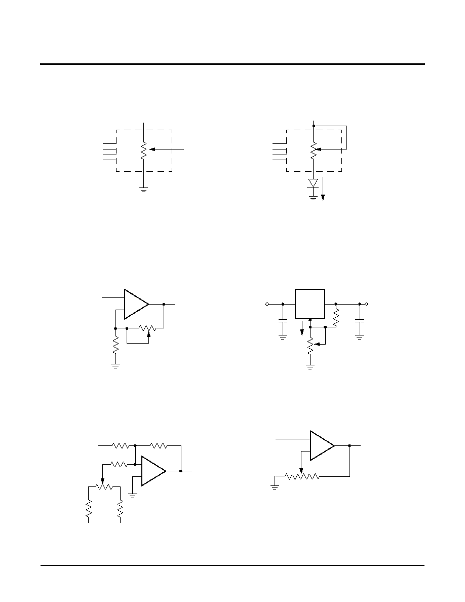
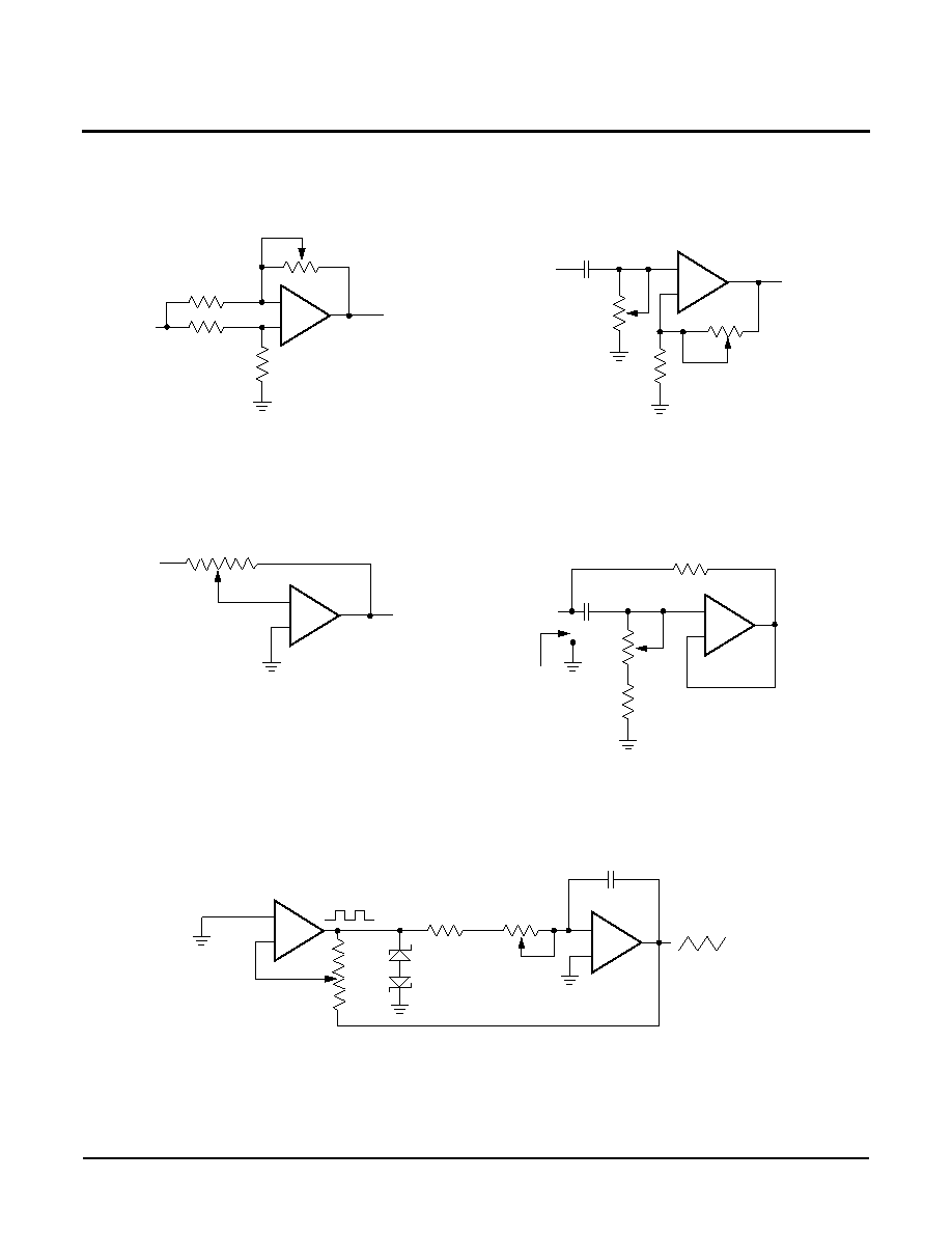
APPLICATIONS INFORMATION
Basic Configurations of Electronic Potentiometers
Application Circuits
V
R
RW
+V
R
I
Three terminal Potentiometer;
Variable voltage divider
Two terminal Variable Resistor;
Variable current
Noninverting Amplifier
Voltage Regulator
Offset Voltage Adjustment
Comparator with Hysterisis
+
≠
V
S
V
O
R
2
R
1
V
O
= (1+R
2
/R
1
)V
S
R
1
R
2
I
adj
V
O
(REG) = 1.25V (1+R
2
/R
1
)+I
adj
R
2
V
O
(REG)
V
IN
317
+
≠
V
S
V
O
R
2
R
1
V
UL
= {R
1
/(R
1
+R
2
)} V
O
(max)
RL
L
= {R
1
/(R
1
+R
2
)} V
O
(min)
100K
10K
10K
10K
-12V
+12V
TL072
+
≠
V
S
V
O
R
2
R
1
}
}
X9119 ≠ Preliminary Information
Characteristics subject to change without notice.
19 of 22
REV 1.1.11 3/12/02
www.xicor.com
Application Circuits (Continued)
Attenuator
Filter
Inverting Amplifier
Equivalent L-R Circuit
+
≠
V
S
V
O
R
3
R
1
V
O
= G V
S
-1/2
G +1/2
G
O
= 1 + R
2
/R
1
fc = 1/(2
RC)
+
≠
V
S
V
O
R
2
R
1
Z
IN
= R
2
+ s R
2
(R
1
+ R
3
) C
1
= R
2
+ s Leq
(R
1
+ R
3
) >> R
2
+
≠
V
S
Function Generator
R
2
R
4
R
1
= R
2
= R
3
= R
4
= 10k
+
≠
V
S
R
2
R
1
R
C
}
}
V
O
= G V
S
G = - R
2
/R
1
R
2
C
1
R
1
R
3
Z
IN
+
≠
R
2
+
≠
R
1
}
}
R
A
R
B
frequency
R
1
, R
2
, C
amplitude
R
A
, R
B
C
V
O
X9119 ≠ Preliminary Information
Characteristics subject to change without notice.
20 of 22
REV 1.1.11 3/12/02
www.xicor.com
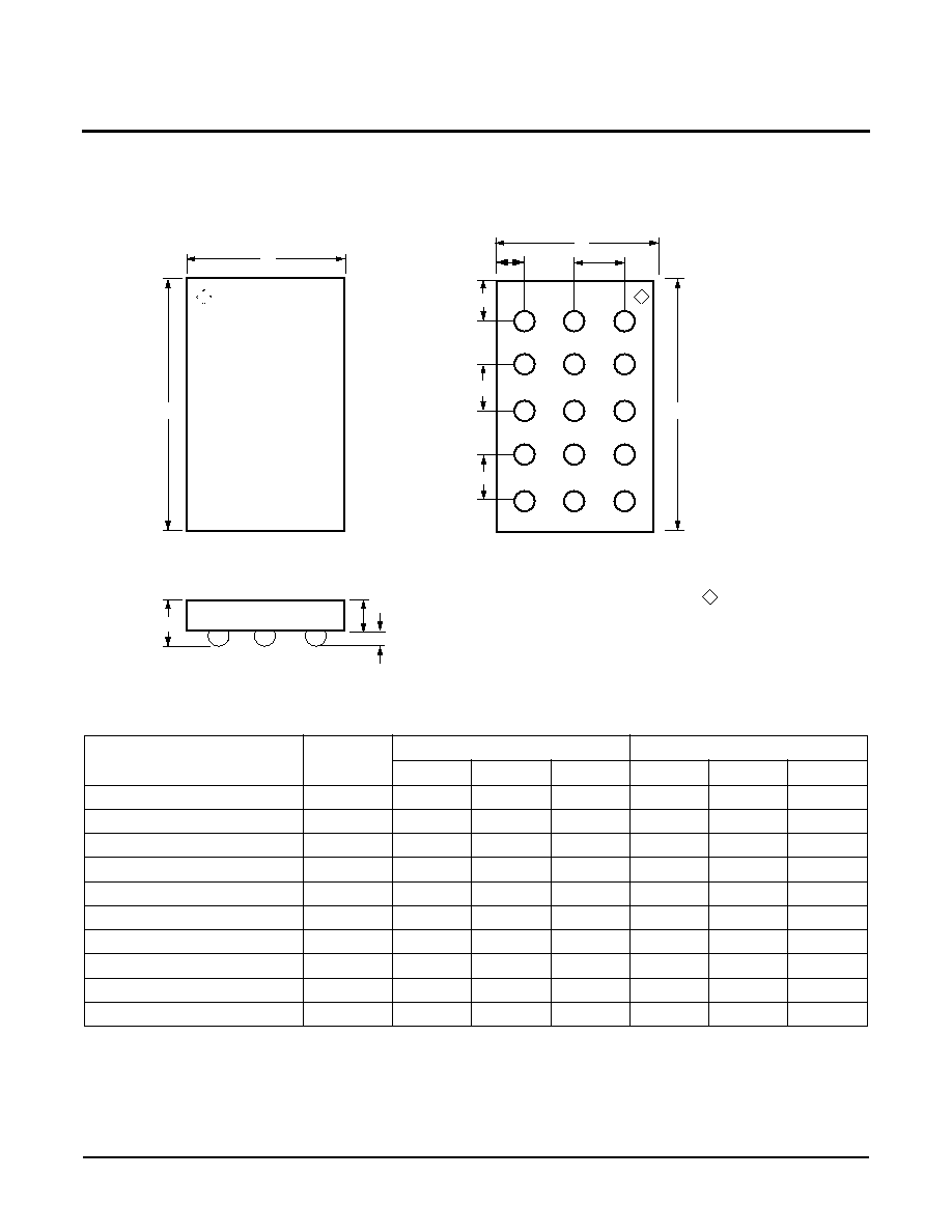
15-ball BGA (X9119TB15)
a
b
Top View (Bump Side Down)
Side View (Bump Side Down)
Bottom View (Bump Side Up)
c
d
e
f
k
a
j
b
Note: Drawing not to scale
= Die Orientation mark
Symbol
Millimeters
Inches
Min
Nom.
Max
Min
Nom.
Max
Package Width
a
2.534
2.564
2.594
0.0998
0.1010
0.1021
Package Length
b
3.271
3.301
3.331
0.1288
0.1300
0.1311
Package Height
c
0.654
0.682
0.710
0.0258
0.0269
0.0280
Body Thickness
d
0.444
0.457
0.470
0.0175
0.0180
0.0185
Ball Height
e
0.210
0.225
0.240
0.0083
0.0089
0.0094
Ball Base Diameter
f
0.270
0.280
0.290
0.0106
0.0110
0.0114
Ball Pitch ≠ Width
j
0.5
0.0197
Ball Pitch ≠ Length
k
0.5
0.0197
Ball to Edge Spacing ≠ Width
l
0.747
0.782
0.817
0.0294
0.0308
0.0322
Ball to Edge Spacing ≠ Length
m
0.615
0.650
0.685
0.0242
0.0256
0.0270
l
m
A
B
C
D
E
1
2
3
X9119 ≠ Preliminary Information
Characteristics subject to change without notice.
21 of 22
REV 1.1.11 3/12/02
www.xicor.com
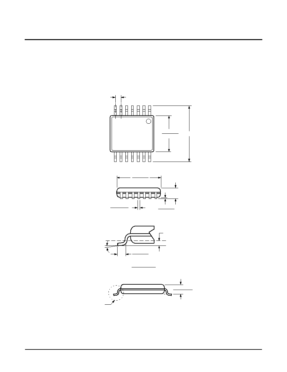
PACKAGING INFORMATION
NOTE: ALL DIMENSIONS IN INCHES (IN PARENTHESES IN MILLIMETERS)
14-Lead Plastic, TSSOP, Package Code V14
See Detail "A"
.031 (.80)
.041 (1.05)
.169 (4.3)
.177 (4.5)
.252 (6.4) BSC
.025 (.65) BSC
.193 (4.9)
.200 (5.1)
.002 (.05)
.006 (.15)
.041 (1.05)
.0075 (.19)
.0118 (.30)
0∞ - 8∞
.010 (.25)
.019 (.50)
.029 (.75)
Gage Plane
Seating Plane
Detail A (20X)

X9119 ≠ Preliminary Information
Characteristics subject to change without notice.
22 of 22
REV 1.1.11 3/12/02
www.xicor.com
LIMITED WARRANTY
Devices sold by Xicor, Inc. are covered by the warranty and patent indemnification provisions appearing in its Terms of Sale only. Xicor, Inc. makes no warranty,
express, statutory, implied, or by description regarding the information set forth herein or regarding the freedom of the described devices from patent infringement.
Xicor, Inc. makes no warranty of merchantability or fitness for any purpose. Xicor, Inc. reserves the right to discontinue production and change specifications and prices
at any time and without notice.
Xicor, Inc. assumes no responsibility for the use of any circuitry other than circuitry embodied in a Xicor, Inc. product. No other circuits, patents, or licenses are implied.
TRADEMARK DISCLAIMER:
Xicor and the Xicor logo are registered trademarks of Xicor, Inc. AutoStore, Direct Write, Block Lock, SerialFlash, MPS, and XDCP are also trademarks of Xicor, Inc. All
others belong to their respective owners.
U.S. PATENTS
Xicor products are covered by one or more of the following U.S. Patents: 4,326,134; 4,393,481; 4,404,475; 4,450,402; 4,486,769; 4,488,060; 4,520,461; 4,533,846;
4,599,706; 4,617,652; 4,668,932; 4,752,912; 4,829,482; 4,874,967; 4,883,976; 4,980,859; 5,012,132; 5,003,197; 5,023,694; 5,084,667; 5,153,880; 5,153,691;
5,161,137; 5,219,774; 5,270,927; 5,324,676; 5,434,396; 5,544,103; 5,587,573; 5,835,409; 5,977,585. Foreign patents and additional patents pending.
LIFE RELATED POLICY
In situations where semiconductor component failure may endanger life, system designers using this product should design the system with appropriate error detection
and correction, redundancy and back-up features to prevent such an occurrence.
Xicor's products are not authorized for use in critical components in life support devices or systems.
1. Life support devices or systems are devices or systems which, (a) are intended for surgical implant into the body, or (b) support or sustain life, and whose failure to
perform, when properly used in accordance with instructions for use provided in the labeling, can be reasonably expected to result in a significant injury to the user.
2. A critical component is any component of a life support device or system whose failure to perform can be reasonably expected to cause the failure of the life
support device or system, or to affect its safety or effectiveness.
©Xicor, Inc. 2000 Patents Pending
ORDERING INFORMATION
Device
V
CC
Limits
Blank = 5V
±10%
≠2.7 = 2.7 to 5.5V
Temperature Range
Blank = Commercial = 0
∞C to +70∞C
I = Industrial = ≠40
∞C to +85∞C
Package
V14 = 14-Lead TSSOP
B15 = 15-Lead XBGA
Potentiometer Organization
Pot
T =
100K
X9119
P
T
V
Y
PART MARK CONVENTION
15 Lead XBGA
Top Mark
X9119TB15I-2.7
XAFF
X9119TB15
XAFC

This datasheet has been download from:
www.datasheetcatalog.com
Datasheets for electronics components.