 | –≠–ª–µ–∫—Ç—Ä–æ–Ω–Ω—ã–π –∫–æ–º–ø–æ–Ω–µ–Ω—Ç: X9241YVI | –°–∫–∞—á–∞—Ç—å:  PDF PDF  ZIP ZIP |
Document Outline
- Table of Contents
- Product Selection
- Data Sheet Alpha
- Ap Note Alpha

X9241
1
Quad E
2
POT
TM
Nonvolatile Digital Potentiometer
© Xicor, Inc. 1994, 1995, 1996 Patents Pending
Characteristics subject to change without notice
3864-2.7 7/1/96 T0/C3/D3 NS
FEATURES
∑
Four E
2
POTs in One Package
∑
Two-Wire Serial Interface
∑
Register Oriented Format
--Directly Write Wiper Position
--Read Wiper Position
--Store as Many as Four Positions per Pot
∑
Instruction Format
--Quick Transfer of Register Contents to
Resistor Array
--Cascade Resistor Arrays
∑
Low Power CMOS
∑
Direct Write Cell
--Endurance - 100,000 Data Changes per Register
--Register Data Retention - 100 years
∑
16 Bytes of E
2
PROM memory
∑
3 Resistor Array Values
--2K
to 50K
Mask Programmable
--Cascadable For Values of 500
to 200K
∑
Resolution: 64 Taps each Pot
∑
20-Lead Plastic DIP, 20-Lead TSSOP and
20-Lead SOIC Packages
X9241
DESCRIPTION
The X9241 integrates four nonvolatile E
2
POT digitally
controlled potentiometers on a monolithic CMOS micro-
circuit.
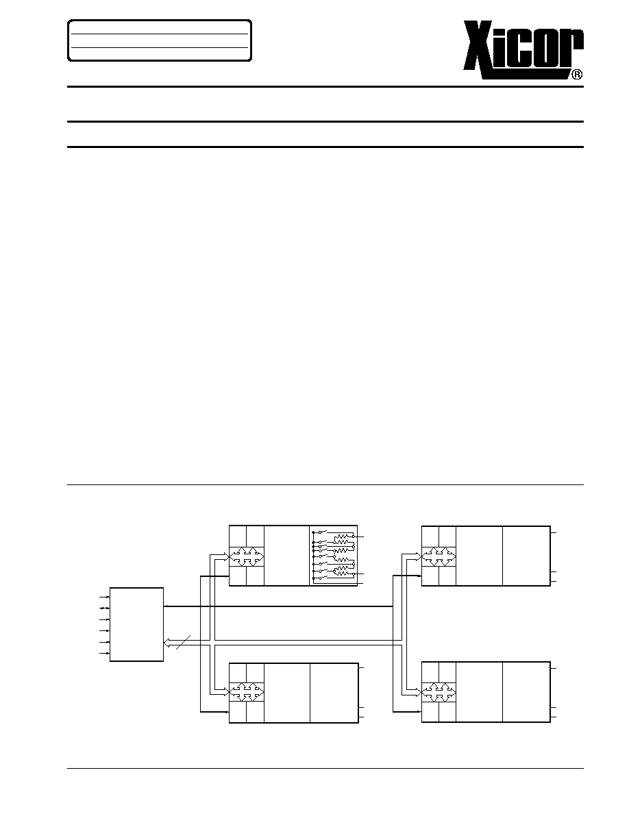
The X9241 contains four resistor arrays, each com-
posed of 63 resistive elements. Between each element
and at either end are tap points accessible to the wiper
elements. The position of the wiper element on the array
is controlled by the user through the two-wire serial bus
interface.
Each resistor array has associated with it a wiper counter
register and four 8-bit data registers that can be directly
written and read by the user. The contents of the wiper
counter register control the position of the wiper on the
resistor array.
The data register may be read or written by the user. The
contents of the data registers can be transferred to the
wiper counter register to position the wiper. The current
wiper position can be transferred to any one of its
associated data registers.
The arrays may be cascaded to form resistive elements
with 127, 190 or 253 taps.
FUNCTIONAL DIAGRAM
Terminal Voltage
±
5V, 64 Taps
A
PPLICATION
N
OTES
AND
D
EVELOPMENT
S
YSTEM
A V A I L A B L E
AN20 ∑ AN42≠48 ∑ AN50≠53 ∑ AN73 ∑ XK9241
3864 ILL F07.1
R0 R1
R2 R3
WIPER
COUNTER
REGISTER
(WCR)
RESISTOR
ARRAY
POT 1
VH1
VL1
VW1
R0 R1
R2 R3
WIPER
COUNTER
REGISTER
(WCR)
R0 R1
R2 R3
WIPER
COUNTER
REGISTER
(WCR)
RESISTOR
ARRAY
POT 2
VH2
VL2
VW2
R0 R1
R2 R3
WIPER
COUNTER
REGISTER
(WCR)
RESISTOR
ARRAY
POT 3
VH3
VL3
VW3
INTERFACE
AND
CONTROL
CIRCUITRY
SCL
SDA
A0
A1
A2
A3
VH0
VL0
VW0
DATA
8

2
X9241
PIN DESCRIPTIONS
Host Interface Pins
Serial Clock (SCL)
The SCL input is used to clock data into and out of the
X9241.
Serial Data (SDA)
SDA is a bidirectional pin used to transfer data into and
out of the device. It is an open drain output and may be
wire-ORed with any number of open drain or open
collector outputs. An open drain output requires the use
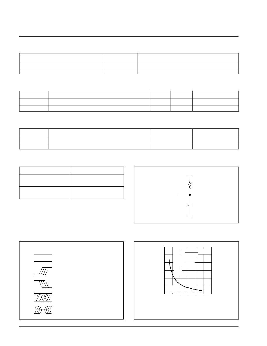
of a pull-up resistor. For selecting typical values, refer
to the guidelines for calculating typical values on the
bus pull-up resistors graph.
Address
The Address inputs are used to set the least significant
4 bits of the 8-bit slave address. A match in the slave
address serial data stream must be made with the
Address input in order to initiate communication with the
X9241.
Potentiometer Pins
V
H
(V
H0
≠ V
H3
), V
L
(V
L0
≠ V
L3
)
The VH and VL inputs are equivalent to the terminal
connections on either end of a mechanical potentiom-
eter.
V
W
(V
W0
≠ V
W3
)
The wiper outputs are equivalent to the wiper output of
a mechanical potentiometer.
PIN CONFIGURATION
PIN NAMES
Symbol
Description
SCL
Serial Clock
SDA
Serial Data
A0≠A3
Address
V
H0
≠V
H3,
V
L0
≠V
L3
Potentiometers
(terminal equivalent)
V
W0
≠V
W3
Potentiometers
(wiper equivalent)
3864 PGM T01
PRINCIPLES OF OPERATION
The X9241 is a highly integrated microcircuit incorporat-
ing four resistor arrays, their associated registers and
counters and the serial interface logic providing direct
communication between the host and the E
2
POT poten-
tiometers.
Serial Interface
The X9241 supports a bidirectional bus oriented proto-
col. The protocol defines any device that sends data
onto the bus as a transmitter and the receiving device as
the receiver. The device controlling the transfer is a
master and the device being controlled is the slave. The
master will always initiate data transfers and provide the
clock for both transmit and receive operations. There-
fore, the X9241 will be considered a slave device in all
applications.
Clock and Data Conventions
Data states on the SDA line can change only during
SCL LOW periods (t
LOW
). SDA state changes during
SCL HIGH are reserved for indicating start and stop
conditions.
Start Condition
All commands to the X9241 are preceded by the start
condition, which is a HIGH to LOW transition of SDA
while SCL is HIGH (t
HIGH
). The X9241 continuously
monitors the SDA and SCL lines for the start condition
and will not respond to any command until this condition
is met.
Stop Condition
All communications must be terminated by a stop con-
dition, which is a LOW to HIGH transition of SDA while
SCL is HIGH.
3864 ILL F01A.2
VW0
VL0
VH0
A0
A2
VW1
VL1
VH1
SDA
VSS
1
2
3
4
5
6
7
8
9
10
20
19
18
17
16
15
14
13
12
11
VCC
VW3
VL3
VH3
A1
A3
SCL
VW2
VL2
VH2
DIP/SOIC/TSSOP
X9241

X9241
3
Acknowledge
Acknowledge is a software convention used to provide
a positive handshake between the master and slave
devices on the bus to indicate the successful receipt of
data. The transmitting device, either the master or the
slave, will release the SDA bus after transmitting eight
bits. The master generates a ninth clock cycle and
during this period the receiver pulls the SDA line LOW to
acknowledge that it successfully received the eight bits
of data. See Figure 7.
The X9241 will respond with an acknowledge after
recognition of a start condition and its slave address and
once again after successful receipt of the command
byte. If the command is followed by a data byte the
X9241 will respond with a final acknowledge.
Array Description
The X9241 is comprised of four resistor arrays. Each
array contains 63 discrete resistive segments that are
connected in series. The physical ends of each array are
equivalent to the fixed terminals of a mechanical poten-
tiometer (V
H
and V
L
inputs).
At both ends of each array and between each resistor
segment is a FET switch connected to the wiper (V
W
)
output. Within each individual array only one switch may
be turned on at a time. These switches are controlled by
the Wiper Counter Register (WCR). The six least signifi-
cant bits of the WCR are decoded to select, and enable,
one of sixty-four switches.
The WCR may be written directly, or it can be changed
by transferring the contents of one of four associated
data registers into the WCR. These data registers and
the WCR can be read and written by the host system.
Device Addressing
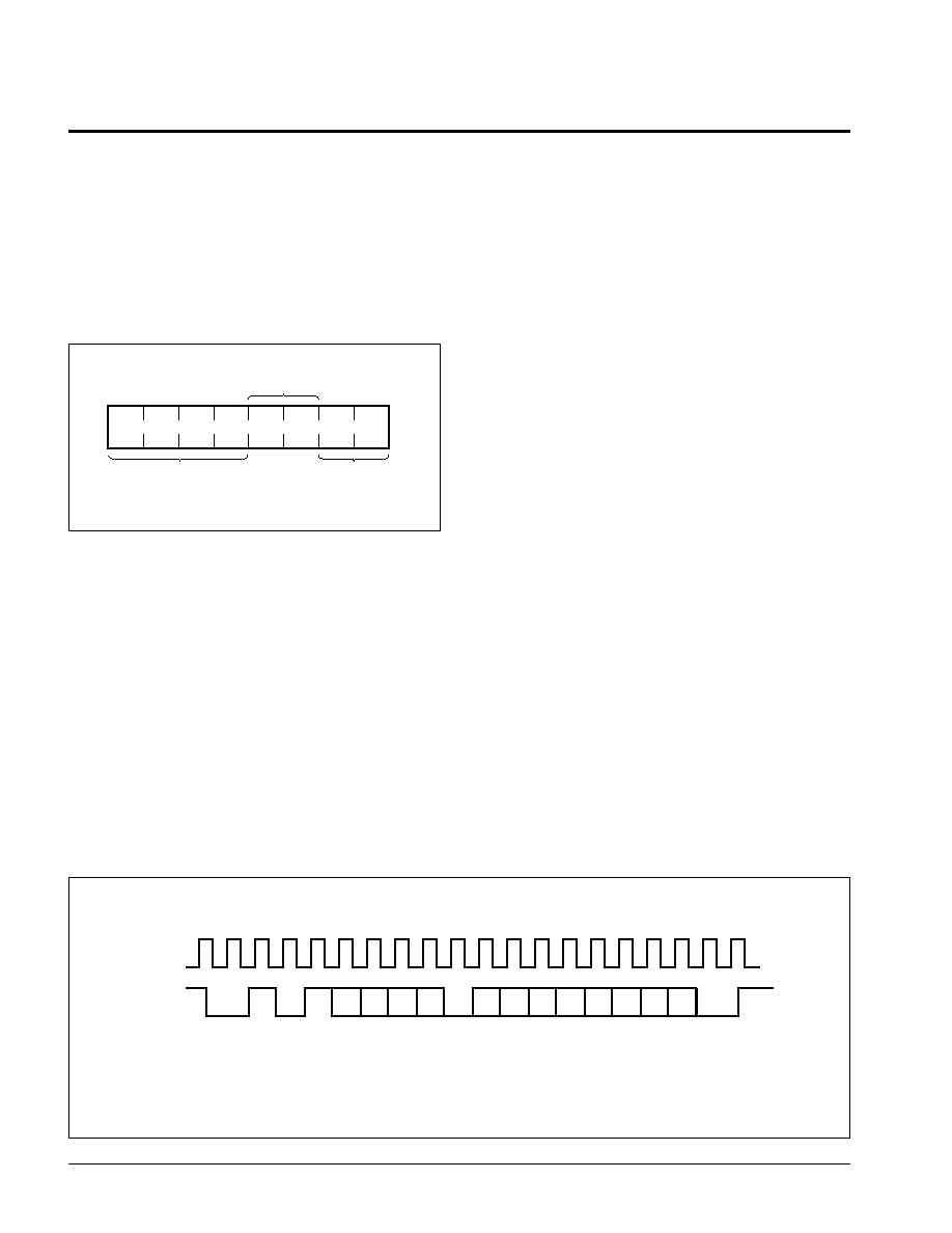
Following a start condition the master must output the
address of the slave it is accessing. The most significant
four bits of the slave address are the device type
identifier (refer to Figure 1 below). For the X9241 this is
fixed as 0101[B].
Figure 1. Slave Address
The next four bits of the slave address are the device
address. The physical device address is defined by the
state of the A0-A3 inputs. The X9241 compares the
serial data stream with the address input state; a suc-
cessful compare of all four address bits is required for
the X9241 to respond with an acknowledge.
Acknowledge Polling
The disabling of the inputs, during the internal non-
volatile write operation, can be used to take advantage
of the typical 5ms E
2
PROM write cycle time. Once the
stop condition is issued to indicate the end of the
nonvolatile write command the X9241 initiates the inter-
nal write cycle. ACK polling can be initiated immediately.
This involves issuing the start condition followed by the
device slave address. If the X9241 is still busy with the
write operation no ACK will be returned. If the X9241 has
completed the write operation an ACK will be returned
and the master can then proceed with the next
operation.
Flow 1. ACK Polling Sequence
NONVOLATILE WRITE
COMMAND COMPLETED
ENTER ACK POLLING
ISSUE
START
ISSUE SLAVE
ADDRESS
ACK
RETURNED?
FURTHER
OPERATION?
ISSUE
INSTRUCTION
PROCEED
ISSUE STOP
NO
YES
YES
PROCEED
ISSUE STOP
NO
3864 ILL F01
1
0
0
A3
A2
A1
A0
DEVICE TYPE
IDENTIFIER
DEVICE ADDRESS
1
3864 FHD F08

4
X9241
Instruction Structure
The next byte sent to the X9241 contains the instruction
and register pointer information. The four most signifi-
cant bits are the instruction. The next four bits point to
one of four pots and when applicable they point to one
of four associated registers. The format is shown below
in Figure 2.
action will be delayed t
STPWV
. A transfer from WCR
current wiper position, to a data register is a write to
nonvolatile memory and takes a minimum of t
WR
to
complete. The transfer can occur between one of the
four potentiometers and one of its associated registers;
or it may occur globally, wherein the transfer occurs
between all four of the potentiometers and one of their
associated registers.
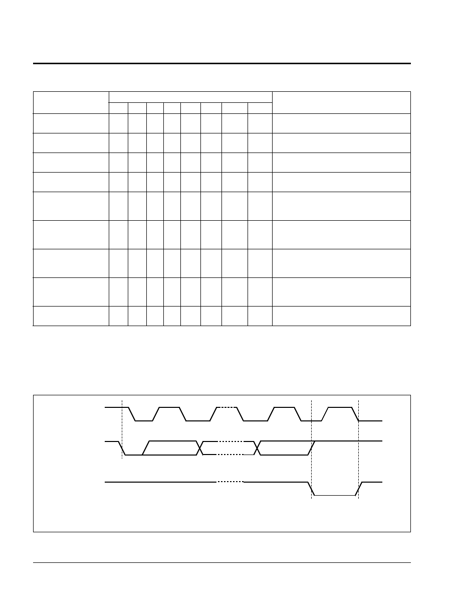
Four instructions require a three-byte sequence to
complete. These instructions transfer data between the
host and the X9241; either between the host and one of
the data registers or directly between the host and the
WCR. These instructions are: Read WCR, read the
current wiper position of the selected pot; Write WCR,
change current wiper position of the selected pot; Read
Data Register, read the contents of the selected non-
volatile register; Write Data Register, write a new value
to the selected data register. The sequence of opera-
tions is shown in Figure 4.
The Increment/Decrement command is different from
the other commands. Once the command is issued and
the X9241 has responded with an acknowledge, the
master can clock the selected wiper up and/or down in
one segment steps; thereby, providing a fine tuning
capability to the host. For each SCL clock pulse (t
HIGH
)
while SDA is HIGH, the selected wiper will move one
resistor segment towards the V
H
terminal. Similarly, for
each SCL clock pulse while SDA is LOW, the selected
wiper will move one resistor segment towards the V
L
terminal. A detailed illustration of the sequence and
timing for this operation are shown in Figures 5 and 6
respectively.
Figure 3. Two-Byte Command Sequence
Figure 2. Instruction Byte Format
The four high order bits define the instruction. The next
two bits (P1 and P0) select which one of the four
potentiometers is to be affected by the instruction. The
last two bits (R1 and R0) select one of the four registers
that is to be acted upon when a register oriented instruc-
tion is issued.
Four of the nine instructions end with the transmission of
the instruction byte. The basic sequence is illustrated in
Figure 3. These two-byte instructions exchange data
between the WCR and one of the data registers. A
transfer from a data register to a WCR is essentially a
write to a static RAM. The response of the wiper to this
I1
3864 ILL F09.1
I2
I3
I0
P1
P0
R1
R0
POTENTIOMETER
SELECT
REGISTER
SELECT
INSTRUCTIONS
3864 ILL F10
S
T
A
R
T
0
1
0
1
A3
A2
A1
A0
A
C
K
I3
I2
I1
I0
P1
P0
R1 R0
A
C
K
SCL
SDA
S
T
O
P

X9241
5
Figure 4. Three-Byte Command Sequence
Figure 6. Increment/Decrement Timing Limits
Figure 5. Increment/Decrement Command Sequence
3864 FHD F12
3864 ILL F11
S
T
A
R
T
0
1
0
1
A3
A2
A1
A0
A
C
K
I3
I2
I1
I0
P1
P0
R1 R0
A
C
K
SCL
SDA
S
T
O
P
A
C
K
CM DW D5 D4
D3
D2
D1 D0
S
T
A
R
T
0
1
0
1
A3
A2
A1
A0
A
C
K
I3
I2
I1
I0
P1 P0
R1 R0
A
C
K
SCL
SDA
S
T
O
P
X
X
I
N
C
1
I
N
C
2
I
N
C
n
D
E
C
1
D
E
C
n
3864 ILL F13
SCL
SDA
VW
INC/DEC
CMD
ISSUED
VOLTAGE OUT
tCLWV

6
X9241
Figure 7. Acknowledge Response from Receiver
Instruction Format
Instruction
I
3
I
2
I
1
I
0
P
1
P
0
R
1
R
o
Operation
Read WCR
1
0
0
1
1/0
(7)
1/0
N/A
(8)
N/A
Read the contents of the Wiper Counter
Register pointed to by P
1
≠P
0
Write WCR
1
0
1
0
1/0
1/0
N/A
N/A
Write new value to the Wiper Counter
Register pointed to by P
1
≠P
0
Read Data
1
0
1
1
1/0
1/0
1/0
1/0
Read the contents of the Register
Register
pointed to by P
1
≠P
0
and R
1
≠R
0
Write Data
1
1
0
0
1/0
1/0
1/0
1/0
Write new value to the Register
Register
pointed to by P
1
≠P
0
and R
1
≠R
0
XFR Data Reg-
1
1
0
1
1/0
1/0
1/0
1/0
Transfer the contents of the Register
ister to WCR
pointed to by P
1
≠P
0
and R
1
≠R
0
to its associated WCR
XFR WCR to
1
1
1
0
1/0
1/0
1/0
1/0
Transfer the contents of the WCR
Data Register
pointed to by P
1
≠P
0
to the Register
pointed to by R
1
≠R
0
Global XFR Data
0
0
0
1
N/A
N/A
1/0
1/0
Transfer the contents of all four Data
Register to WCR
Registers pointed to by R
1
≠R
0
to their
respective WCR
Global XFR WCR
1
0
0
0
N/A
N/A
1/0
1/0
Transfer the contents of all WCRs
to Data Register
to their respective data Registers
pointed to by R
1
≠R
0
Increment/Decre-
0
0
1
0
1/0
1/0
N/A
N/A
Enable Increment/decrement of the
ment Wiper
WCR pointed to by P
1
≠P
0
3864 PGM T02.1
Table 1. Instruction Set
Notes: (7) 1/0 = data is one or zero
(8) N/A = Not applicable or don't care; that is, a data register is not involved in the operation and need not be addressed (typical)
3864 ILL F14
SCL FROM
MASTER
DATA
OUTPUT
FROM
TRANSMITTER
1
8
9
DATA
OUTPUT
FROM
RECEIVER
START
ACKNOWLEDGE

X9241
7
DETAILED OPERATION
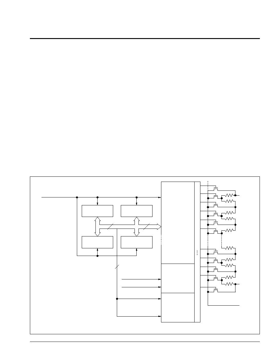
All four E
2
POT potentiometers share the serial interface
and share a common architecture. Each potentiometer
is comprised of a resistor array, a wiper counter register
and four data registers. A detailed discussion of the
register organization and array operation follows.
Wiper Counter Register
The X9241 contains four wiper counter registers (WCR),
one for each E
2
POT potentiometer. The WCR can be
envisioned as a 6-bit parallel and serial load counter with
its outputs decoded to select one of sixty-four switches
along its resistor array. The contents of the WCR can be
altered in four ways: it may be written directly by the host
via the Write WCR instruction (serial load); it may be
written indirectly by transferring the contents of one of
four associated data registers via the XFR Data Register
instruction (parallel load); it can be modified one step at
a time by the Increment/ Decrement instruction; finally,
it is loaded with the contents of its data register zero (R0)
upon power-up.
The WCR is a volatile register; that is, its contents are
lost when the X9241 is powered-down. Although the
register is automatically loaded with the value in R0
upon power-up, it should be noted this may be different
from the value present at power-down.
Data Registers
Each potentiometer has four
nonvolatile data registers.
These can be read or written directly by the host and
data can be transferred between any of the four data
registers and the WCR. It should be noted all operations
changing data in one of these registers is a nonvolatile
operation and will take a maximum of 10ms.
If the application does not require storage of multiple
settings for the potentiometer, these registers can be
used as regular memory locations that could possibly
store system parameters or user preference data.
Figure 8. Detailed Potentiometer Block Diagram
3864 ILL F15
SERIAL DATA PATH
FROM INTERFACE
CIRCUITRY
REGISTER 0
REGISTER 1
REGISTER 2
REGISTER 3
SERIAL
BUS
INPUT
PARALLEL
BUS
INPUT
WIPER
COUNTER
REGISTER
INC/DEC
LOGIC
CASCADE
CONTROL
LOGIC
UP/DN
CLK
MODIFIED SCL
UP/DN
DW
CM
VH
VL
VW
IF WCR = 00[H] THEN VW = VL
IF WCR = 3F[H] THEN VW = VH
2
8
6
C
O
U
N
T
E
R
D
E
C
O
D
E

8
X9241
Cascade Mode
The X9241 provides a mechanism for cascading the
arrays. That is, the sixty-three resistor elements of one
array may be cascaded (linked) with the resistor ele-
ments of an adjacent array.
Cascade Control Bits
The data byte, for the three-byte commands, contains 6
bits (LSBs) for defining the wiper position plus two high
order bits, CM (Cascade Mode) and DW (Disable Wiper).
The state of CM enables or disables (normal operation)
cascade mode. When the CM bit of the WCR is set to "0"
the potentiometer is in the normal operation mode.
When the CM bit of the WCR is set to "1" the potentiometer
is cascaded with its adjacent higher order potentiometer.
For example; if bit 7 of WCR2 is set to "1", pot 2 will be
cascaded to pot 3.
The state of DW enables or disables the wiper. When the
Figure 9. Cascading Arrays
DW bit of the WCR is set to "0" the wiper is enabled;
when set to "1" the wiper is disabled. If the wiper is
disabled, the wiper terminal will be electrically isolated
and float.
When operating in cascade mode VH, VL and the wiper
terminals of the cascaded arrays must be electrically
connected externally. All but one of the wipers must be
disabled. The user can alter the wiper position by writing
directly to the WCR or indirectly by transferring the
contents of the data registers to the WCR or by using the
Increment/Decrement command.
When using the Increment/Decrement command the
wiper position will automatically transition between
arrays. The current position of the wiper can be deter-
mined by reading the WCR registers; if the DW bit is "0",
the wiper in that array is active. If the current wiper
position is to be maintained, a global XFR WCR to Data
Register command must be issued before power-down.
3864 ILL F16.1
VH0
VL0
VW0
VL1
VH1
VW1
VL2
VH2
VW2
VL3
VH3
VW3
POT 0
WCR0
POT 1
WCR1
POT 2
WCR2
POT 3
WCR3
EXTERNAL
CONNECTION
=

X9241
9
Notes: (1) Absolute Linearity is utilized to determine actual wiper voltage versus expected voltage as determined by wiper
position when used as a potentiometer.
(2) Relative Linearity is utilized to determine the actual change in voltage between two successive tap positions when used as a
potentiometer. It is a measure of the error in step size.
(3) MI = RTOT/63 or (V
H
≠ V
L
)/63, single pot
(4) Max. = all four arrays cascaded together, Typical = individual array resolutions.
ABSOLUTE MAXIMUM RATINGS*
Temperature under Bias .................. ≠65
∞
C to +135
∞
C
Storage Temperature ....................... ≠65
∞
C to +150
∞
C
Voltage on SCK, SCL or any Address Input
with Respect to V
SS ...................................
≠1V to +7V
Voltage on any V
H
or V
L
Referenced to V
SS .........
±
8V
V = |V
H
≠V
L
| ......................................................... 16V
Lead Temperature (Soldering, 10 seconds) ...... 300
∞
C
*COMMENT
Stresses above those listed under "Absolute Maximum
Ratings" may cause permanent damage to the device.
This is a stress rating only and the functional operation of
the device at these or any other conditions above those
indicated in the operational sections of this specification is
not implied. Exposure to absolute maximum rating condi-
tions for extended periods may affect device reliability.
RECOMMENDED OPERATING CONDITIONS
Temperature
Min.
Max.
Commercial
0
∞
C
+70
∞
C
Industrial
≠40
∞
C
+85
∞
C
Military
≠55
∞
C
+125
∞
C
3864 PGM T03
Supply Voltage
Limits
X9241
5V
±
10%
3864 PGM T04.1
ANALOG CHARACTERISTICS (Over recommended operating conditions unless otherwise stated.)
Limits
Symbol
Parameter
Min.
Typ.
Max.
Units
Test Conditions
R
TOTAL
End to End Resistance
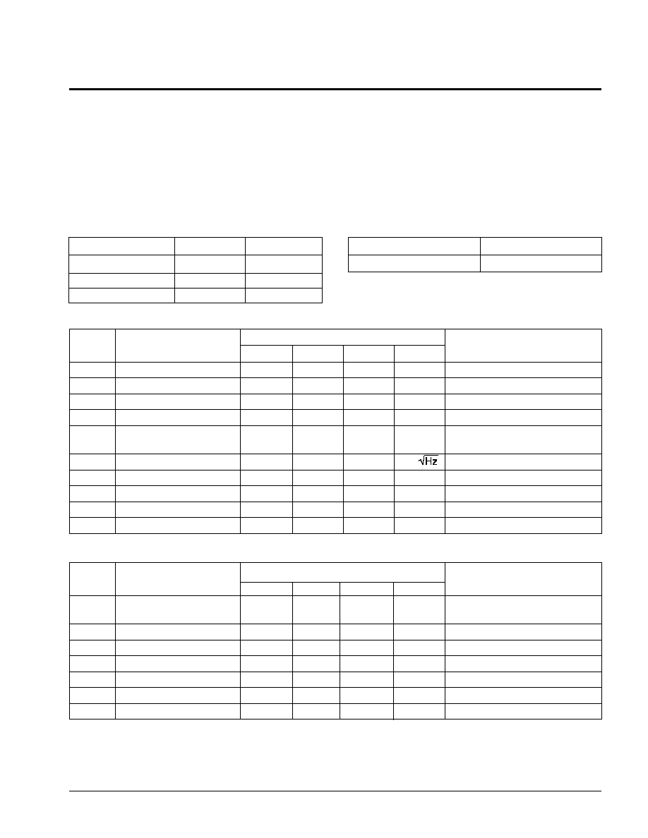
≠20
+20
%
Power Rating
50
mW
25
∞
C, each pot
I
W
Wiper Current
≠1
+1
mA
R
W
Wiper Resistance
40
100
Wiper Current =
±
1mA
V
TERM
Voltage on any V
H
or
≠5
+5
V
or V
L
Pin
Noise
120
dB/
Ref: 1V
Resolution
(4)
1.6
0.4
%
Absolute Linearity
(1)
≠1
+1
MI
(3)
V
w(n)(actual)
≠ V
w(n)(expected)
Relative Linearity
(2)
≠0.2
+0.2
MI
(3)
V
w(n + 1)
≠ [V
w(n) + MI
]
Temperature Coefficient
±
300
ppm/
∞
C
3864 PGM T05.2
D.C. OPERATING CHARACTERISTICS (Over recommended operating conditions unless otherwise stated.)
Limits
Symbol
Parameter
Min.
Typ.
Max.
Units
Test Conditions
l
CC
Supply Current (Active)
3
mA
f
SCL
= 100KHz, SDA = Open,
Other Inputs = V
SS
I
SB
V
CC
Current (Standby)
200
500
µ
A
SCL=SDA=V
CC
, Addr. = V
SS
I
LI
Input Leakage Current
10
µ
A
V
IN
= V
SS
to V
CC
I
LO
Output Leakage Current
10
µ
A
V
OUT
= V
SS
to V
CC
V
IH
Input HIGH Voltage
2
V
CC
+ 1
V
V
IL
Input LOW Voltage
≠1
0.8
V
V
OL
Output LOW Voltage
0.4
V
I
OL
= 3mA
3864 PGM T06.3

10
X9241
Guidelines for Calculating
Typical Values of Bus Pull-Up Resistors
CAPACITANCE
Symbol
Parameter
Max.
Units
Test Conditions
C
I/O
(5)
Input/Output Capacitance (SDA)
8
pF
V
I/O
= 0V
C
IN
(5)
Input Capacitance (A0, A1, A2, A3 and SCL)
6
pF
V
IN
= 0V
3864 PGM T08
POWER-UP TIMING
Symbol
Parameter
Max.
Units
t
PUR
(6)
Power-up to Initiation of Read Operation
1
ms
t
PUW
(6)
Power-up to Initiation of Write Operation
5
ms
3864 PGM T09
A.C. CONDITIONS OF TEST
Input Pulse Levels
V
CC
x 0.1 to V
CC
x 0.9
Input Rise and
Fall Times
10ns
Input and Output
Timing Levels
V
CC
x 0.5
3864 PGM T10
EQUIVALENT A.C. TEST CIRCUIT
Notes: (5) This parameter is periodically sampled and not 100%
tested.
(6) t
PUR
and t
PUW
are the delays required from the time
VCC is stable until the specified operation can be
initiated. These parameters are periodically sampled
and not 100% tested.
3864 ILL F02.1
5V
1533
100pF
SDA OUTPUT
3864 ILL F17
120
100
80
40
60
20
20
40
60
80 100 120
0
0
RESIST
ANCE (K
)
BUS CAPACITANCE (pF)
MIN.
RESISTANCE
MAX.
RESISTANCE
RMAX =
CBUS
tR
RMIN =
IOL MIN
VCC MAX
=1.8K
SYMBOL TABLE
WAVEFORM
INPUTS
OUTPUTS
Must be
steady
Will be
steady
May change
from LOW
to HIGH
Will change
from LOW
to HIGH
May change
from HIGH
to LOW
Will change
from HIGH
to LOW
Don't Care:
Changes
Allowed
Changing:
State Not
Known
N/A
Center Line
is High
Impedance
ENDURANCE AND DATA RETENTION
Parameter
Min.
Units
Minimum Endurance
100,000
Data Changes per Register
Data Retention
100
Years
3864 PGM T07.2

X9241
11
Limits
Reference
Symbol
Parameter
Min.
Max.
Units
Figure
f
SCL
SCL Clock Frequency
0
100
KHz
10
t
LOW
Clock LOW Period
4700
ns
10
t
HIGH
Clock HIGH Period
4000
ns
10
t
R
SCL and SDA Rise Time
1000
ns
10
t
F
SCL and SDA Fall Time
300
ns
10
Ti
Noise Suppression Time Constant
100
ns
10
(Glitch Filter)
t
SU:STA
Start Condition Setup Time (for a Repeated
4700
ns
10 & 12
Start Condition)
t
HD:STA
Start Condition Hold Time
4000
ns
10 & 12
t
SU:DAT
Data in Setup Time
250
ns
10
t
HD:DAT
Data in Hold Time
0
ns
10
t
AA
SCL LOW to SDA Data Out Valid
300
3500
ns
11
t
DH
Data Out Hold Time
300
ns
11
t
SU:STO
Stop Condition Setup Time
4700
ns
10 & 12
t
BUF
Bus Free Time Prior to New Transmission
4700
ns
10
t
WR
Write Cycle Time (Nonvolatile Write Operation)
10
ms
13
t
STPWV
Wiper Response Time From Stop Generation
500
µ
s
13
t
CLWV
Wiper Response From SCL LOW
1000
µ
s
6
t
R
V
CC
V
CC
Power-up Rate
0.2
50
mV/
µ
s
3864 PGM T11.3
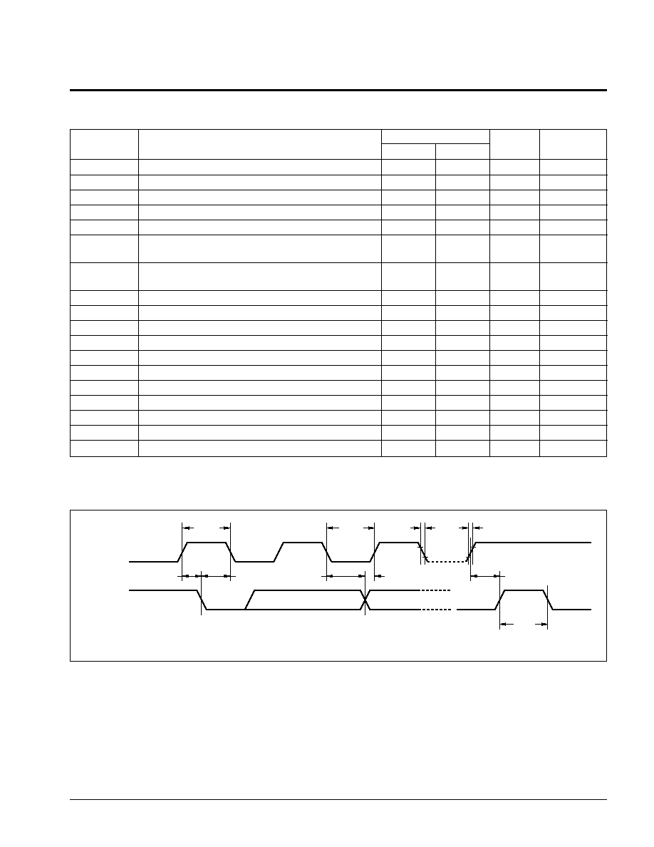
A.C. CHARACTERISTICS (Over recommended operating conditions unless otherwise stated)
Figure 10. Input Bus Timing
3864 ILL F03
tHIGH
tSU:STA
tHD:STA
tHD:DAT
tSU:DAT
tLOW
tF
tSU:STO
tR
tBUF
SCL
SDA
(DATA IN)

12
X9241
Figure 11. Output Bus Timing
Figure 12. Start Stop Timing
Figure 13. Write Cycle and Wiper Response Timing
3864 ILL F04
tAA
tDH
SCL
SDA
SDA OUT (ACK)
SDA OUT
SDA OUT
3864 ILL F05
tSU:STO
SCL
SDA
DATA IN
tHD:STA
tSU:STA
STOP CONDITION
START CONDITION
3864 ILL F06
SCL
SDA
WIPER
OUTPUT
CLOCK 8
SDAIN
CLOCK 9
ACK
STOP
tWR
tSTPWV
START

X9241
13
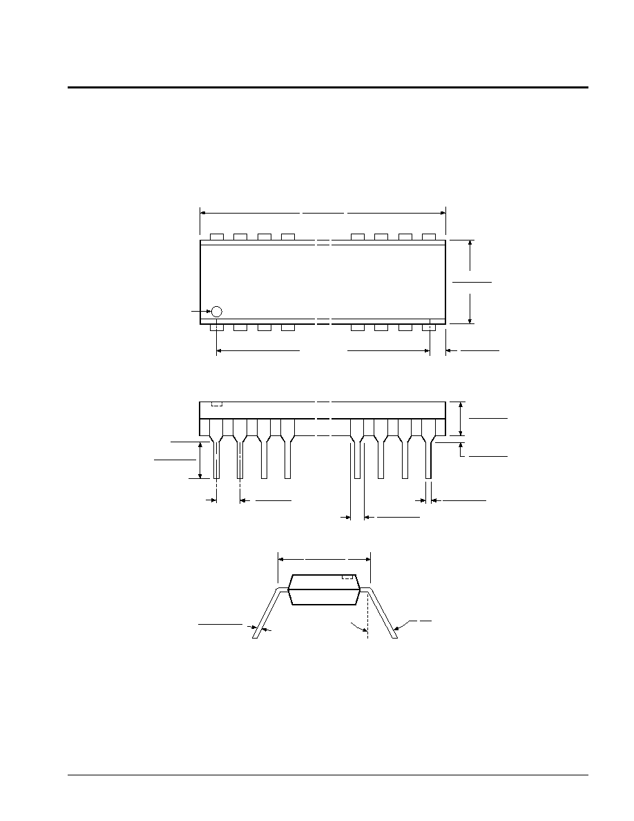
PACKAGING INFORMATION
0.022 (0.559)
0.014 (0.356)
(3.81) 0.150
(2.92) 0.1150
0.10 (BSC)
(2.54)
1.060 (26.92)
0.980 (24.89)
0.900 (23.66)
REF.
PIN 1 INDEX
0.195 (4.95)
0.115 (2.92)
≠≠
0.015 (0.38)
3926 FHD F18.1
PIN 1
SEATING
PLANE
0.070 (1.778)
0.045 (1.143)
0.280 (7.11)
0.240 (6.096)
--
0.005 (0.127)
0
∞
15
∞
20-LEAD PLASTIC DUAL IN-LINE PACKAGE TYPE P
NOTE:
1. ALL DIMENSIONS IN INCHES (IN PARENTHESES IN MILLIMETERS)
2. PACKAGE DIMENSIONS EXCLUDE MOLDING FLASH
0.014 (0.356)
0.008 (0.2032)
0.300
(7.62) (BSC)

14
X9241
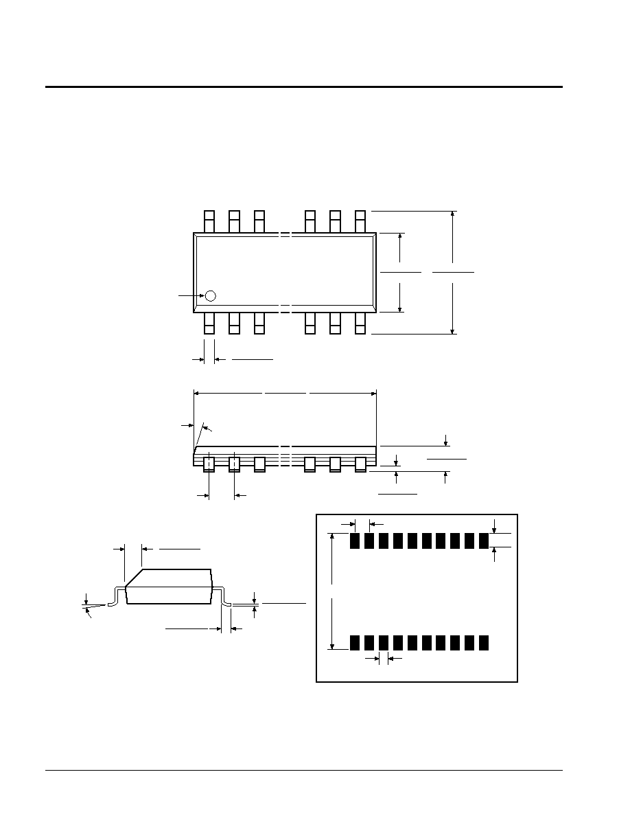
PACKAGING INFORMATION
0.290 (7.37)
0.299 (7.60)
0.393 (10.00)
0.420 (10.65)
0.014 (0.35)
0.020 (0.50)
PIN 1
PIN 1 INDEX
0.010 (0.25)
0.020 (0.50)
0.050 (1.27)
0.496 (12.60)
0.508 (12.90)
0.003 (0.10)
0.012 (0.30)
0.092 (2.35)
0.105 (2.65)
(4X) 7
∞
0.015 (0.40)
0.050 (1.27)
0.007 (0.18)
0.011 (0.28)
0
∞
≠ 8
∞
X 45
∞
3926 FHD F23
20-LEAD PLASTIC SMALL OUTLINE GULL WING PACKAGE TYPE S
NOTE: ALL DIMENSIONS IN INCHES (IN PARENTHESES IN MILLIMETERS)
0.420"
0.050" Typical
0.050"
Typical
0.030" Typical
20 Places
FOOTPRINT

X9241
15
PACKAGING INFORMATION
NOTE: ALL DIMENSIONS IN INCHES (IN PARENTHESES IN MILLIMETERS)
20-LEAD PLASTIC, TSSOP PACKAGE TYPE V
See Detail "A"
.031 (.80)
.041 (1.05)
.169 (4.3)
.177 (4.5)
.252 (6.4) BSC
.025 (.65) BSC
.252 (6.4)
.300 (6.6)
.002 (.05)
.006 (.15)
.047 (1.20)
.0075 (.19)
.0118 (.30)
0
∞
≠ 8
∞
.010 (.25)
.019 (.50)
.029 (.75)
Gage Plane
Seating Plane
Detail A (20X)
3926 FHD F45

16
X9241
ORDERING INFORMATION
LIMITED WARRANTY
Devices sold by Xicor, Inc. are covered by the warranty and patent indemnification provisions appearing in its Terms of Sale only. Xicor, Inc. makes no warranty,
express, statutory, implied, or by description regarding the information set forth herein or regarding the freedom of the described devices from patent infringement.
Xicor, Inc. makes no warranty of merchantability or fitness for any purpose. Xicor, Inc. reserves the right to discontinue production and change specifications and
prices at any time and without notice.
Xicor, Inc. assumes no responsibility for the use of any circuitry other than circuitry embodied in a Xicor, Inc. product. No other circuits, patents, licenses are
implied.
U.S. PATENTS
Xicor products are covered by one or more of the following U.S. Patents: 4,263,664; 4,274,012; 4,300,212; 4,314,265; 4,326,134; 4,393,481; 4,404,475;
4,450,402; 4,486,769; 4,488,060; 4,520,461; 4,533,846; 4,599,706; 4,617,652; 4,668,932; 4,752,912; 4,829, 482; 4,874, 967; 4,883, 976. Foreign patents and
additional patents pending.
LIFE RELATED POLICY
In situations where semiconductor component failure may endanger life, system designers using this product should design the system with appropriate error
detection and correction, redundancy and back-up features to prevent such an occurrence.
Xicor's products are not authorized for use in critical components in life support devices or systems.
1. Life support devices or systems are devices or systems which, (a) are intended for surgical implant into the body, or (b) support or sustain life, and whose
failure to perform, when properly used in accordance with instructions for use provided in the labeling, can be reasonably expected to result in a significant
injury to the user.
2. A critical component is any component of a life support device or system whose failure to perform can be reasonably expected to cause the failure of the life
support device or system, or to affect its safety or effectiveness.
Device
V
CC
Limits
Blank = 5V
±
10%
Temperature Range
Blank = Commercial = 0
∞
C to +70
∞
C
I = Industrial = ≠40
∞
C to +85
∞
C
M = Military = ≠55
∞
C to +125
∞
C
Package
P = 20-Lead Plastic DIP
S = 20-Lead SOIC
V = 20-Lead TSSOP
Potentiometer Organization
Pot 0 Pot 1 Pot 2 Pot 3
Y = 2K
2K
2K
2K
W = 10K
10K
10K
10K
U = 50K
50K
50K
50K
M = 2K
10K
10K
50K
X9241 Y P T V
