 | –≠–ª–µ–∫—Ç—Ä–æ–Ω–Ω—ã–π –∫–æ–º–ø–æ–Ω–µ–Ω—Ç: X9316ZP3 | –°–∫–∞—á–∞—Ç—å:  PDF PDF  ZIP ZIP |
Document Outline
- Table of Contents
- Product Selection
- Data Sheet Alpha
- Ap Note Alpha
©
Xicor, Inc. 1994, 1995, 1996 Patents Pending
7000-1.5 7/16/97 T6/C0/D6 SH
1
Characteristics subject to change without notice
X9316
E
2
POTTM Nonvolatile Digital Potentiometer
FEATURES
∑ Low Micropower CMOS
--V
CC
= 3V to 5.5V
--Active Current, 50
µ
A (Increment) Max
--Standby Current, 400
µ
A (Store) Max
∑ Low Noise
∑ 31 Resistive Elements
--Temperature Compensated
--
±
20% End to End Resistance Range
--≠5V to +5V
∑ 32 Wiper Tap Points
--Wiper Positioned via Three-Wire Interface
--Similar to TTL Up/Down Counter
--Wiper Position Stored in Nonvolatile
Memory and Recalled on Power-Up
∑ 100 Year Wiper Position Data Retention
∑ X9316Z = 1K
∑ X9316W = 10K
∑ Packages
--14-Lead PDIP
--14-Lead SOIC
DESCRIPTION
The Xicor X9316 is a solid state "micropower" nonvolatile
potentiometer and is ideal for digitally controlled resis-
tance trimming in battery-powered systems.
The X9316 is a resistor array composed of 31 resistive
elements. Between each element and at either end are
tap points accessible to the wiper element. The position
of the wiper element is controlled by the CS, U/D, and
INC inputs. The position of the wiper can be stored in
nonvolatile memory and then be recalled upon a subse-
quent power-up operation.
The resolution of the X9316 is equal to the maximum
resistance value divided by 31. As an example, for the
X9316W (10K
) each tap point represents 323
.
All Xicor nonvolatile memories are designed and tested
for applications requiring extended endurance and data
retention.
Low Noise, Low Power, 32 Taps
FUNCTIONAL DIAGRAM
7000 FRM F01
5-BIT
UP/DOWN
COUNTER
5-BIT
NONVOLATILE
MEMORY
STORE AND
RECALL
CONTROL
CIRCUITRY
ONE
OF
THIRTY-
TWO
WIPER
POSITION
DECODER
RESISTOR
ARRAY
V
L
V
W
V
H
U/D
INC
CS
V
CC
V
SS
CMOS SWITCH
V+
V≠
E2POTTM is a trademark of Xicor, Inc.
X9316
2
PIN DESCRIPTIONS
V
H
and V
L
The high (V
H
) and low (V
L
) terminals of the X9316 are
equivalent to the fixed terminals of a mechanical potenti-
ometer. The minimum voltage is V
≠
and the maximum is
V
+
. It should be noted that the terminology of V
L
and V
H
references the relative position of the terminal in relation
to wiper movement direction selected by the U/D input
and not the voltage potential on the terminal.
V
W
V
W
is the wiper terminal, equivalent to the movable termi-
nal of a mechanical potentiometer. The position of the
wiper within the array is determined by the control inputs.
The wiper terminal series resistance is typically 100
.
Up/Down (U/D)
The U/D input controls the direction of the wiper move-
ment and whether the counter is incremented or decre-
mented.
Increment (INC)
The INC input is negative-edge triggered. Toggling INC
will move the wiper and either increment or decrement
the counter in the direction indicated by the logic level on
the U/D input.
Chip Select (CS)
The device is selected when the CS input is LOW. The
current counter value is stored in nonvolatile memory
when CS is returned HIGH while the INC input is also
HIGH. After the store operation is complete, the X9316
will be placed in the low power standby mode until the
device is selected once again.
V
+
, V
≠
(Analog positive/negative power supply)
The V
+
and V
≠
pins supply an external voltage to the
wiper position decoder.
PIN CONFIGURATION
PIN NAMES
7000 FRM T01.1
Symbol
Description
V
H
High Terminal
V
W
Wiper Terminal
V
L
Low Terminal
V
SS
Ground
V
CC
Supply Voltage
U/D
Up/Down Input
INC
Increment Input
CS
Chip Select Input
V
+
Positive Analog Voltage
V
≠
Negative Analog Voltage
14-LEAD DIP/SOIC
NC
V
CC
CS
V
L
V
W
V+
NC
7000 FRM 02
NC
INC
U/D
V
H
V
SS
V
≠
NC
1
2
3
4
5
6
7
14
13
12
11
10
9
8
X9316
X9316
3
DEVICE OPERATION
There are three sections of the X9316: the input control,
counter and decode section; the nonvolatile memory;
and the resistor array. The input control section operates
just like an up/down counter. The output of this counter is
decoded to turn on a single electronic switch connecting
a point on the resistor array to the wiper output. Under
the proper conditions the contents of the counter can be
stored in nonvolatile memory and retained for future use.
The resistor array is comprised of 31 individual resistors
connected in series. At either end of the array and
between each resistor is an electronic switch that trans-
fers the potential at that point to the wiper.
The INC, U/D and CS inputs control the movement of the
wiper along the resistor array. With CS set LOW the
X9316 is selected and enabled to respond to the U/D
and INC inputs. HIGH to LOW transitions on INC will
increment or decrement (depending on the state of the
U/D input) a seven bit counter. The output of this counter
is decoded to select one of thirty two wiper positions
along the resistive array.
The wiper, when at either fixed terminal, acts like its
mechanical equivalent and does not move beyond the
last position. That is, the counter does not wrap around
when clocked to either extreme.
The value of the counter is stored in nonvolatile memory
whenever CS transistions HIGH while the INC input is
also HIGH.
When the X9316 is powered-down, the last counter posi-
tion stored will be maintained in the nonvolatile memory.
When power is restored, the contents of the memory are
recalled and the counter is reset to the value last stored.
Operation Notes
The system may select the X9316, move the wiper and
deselect the device without having to store the latest
wiper position in nonvolatile memory. The wiper move-
ment is performed as described above; once the new
position is reached, the system would the keep INC LOW
while taking CS HIGH. The new wiper position would be
maintained until changed by the system or until a power-
up/down cycle recalled the previously stored data.
This would allow the system to always power-up to a pre-
set value stored in nonvolatile memory; then during sys-
tem operation minor adjustments could be made. The
adjustments might be based on user preference, system
parameter changes due to temperature drift, etc...
The state of U/D may be changed while CS remains
LOW. This allows the host system to enable the X9316
and then move the wiper up and down until the proper
trim is attained.
T
IW
/R
TOTAL
The electronic switches on the X9316 operate in a "make
before break" mode when the wiper changes tap posi-
tions. If the wiper is moved several positions multiple taps
are connected to the wiper for t
IW
(INC to V
W
change).
The R
TOTAL
value for the device can temporarily be
reduced by a significant amount if the wiper is moved
several positions.
SYMBOL TABLE
WAVEFORM
INPUTS
OUTPUTS
Must be
steady
Will be
steady
May change
from Low to
High
Will change
from Low to
High
May change
from High to
Low
Will change
from High to
Low
Don't Care:
Changes
Allowed
Changing:
State Not
Known
N/A
Center Line
is High
Impedance
X9316
4
ABSOLUTE MAXIMUM RATINGS*
Temperature under Bias ................... ≠65
∞
C to +135
∞
C
Storage Temperature........................ ≠65
∞
C to +150
∞
C
Voltage on CS, INC, U/D and VCC
with Respect to VSS............................ ≠1V to +7V
Voltage on VH and VL Referenced to VSS
V = |VH≠VL|
X9316Z ..............................................................4V
X9316W...........................................................10V
Lead Temperature (Soldering 10 seconds) ....... 300
∞
C
Wiper Current.....................................................
±
1mA
ANALOG CHARACTERISTICS
Electrical Characteristics
End-to-End Resistance Tolerance ....................
±
20%
Power Rating at 25
∞
C
X9316Z ........................................................16mW
X9316W.......................................................10mW
Wiper Current ...........................................
±
1mA Max.
Typical Wiper Resistance ...................... 100
at 1mA
Typical Noise ............................ < ≠140dB
Hz Ref: 1V
Resolution
Resistance ............................................................. 3%
Linearity
Absolute Linearity
(1)
....................................
±
1.0 Ml
(2)
Relative Linearity
(3)
....................................
±
0.2 Ml
(2)
*COMMENT
Stresses above those listed under "Absolute Maximum
Ratings" may cause permanent damage to the device.
This is a stress rating only and the functional operation of
the device at these or any other conditions above those
listed in the operational sections of this specification is
not implied. Exposure to absolute maximum rating condi-
tions for extended periods may affect device reliability.
Temperature Coefficient
(≠40
∞
C to +85
∞
C) ........................+300 ppm/
∞
C Typical
Ratiometric Temperature Coefficient ............
±
20 ppm
Wiper Adjustability
Unlimited Wiper Adjustment (Non-Store operation)
Wiper Position Store Operations .............. 100,000
Physical Characteristics
Marking Includes
Manufacturer's Trademark
Resistance Value or Code
Date Code
Test Circuit #1
Test Circuit #2
7000 FRM 03
TEST POINT
V
W
V
H
V
L
7000 FRM F04
FORCE
CURRENT
V
L
V
W
V
H
TEST POINT
Notes:
(1) Absolute Linearity is utilized to determine actual wiper voltage versus expected voltage
= (V
w(n)
(actual) ≠ V
w(n)
(expected)) =
±
1 Ml Maximum.
(2) 1 Ml = Minimum Increment = R
TOT
/31.
(3) Relative Linearity is a measure of the error in step size between taps = V
W(n+1)
≠ [V
w(n)
+ Ml] = +0.2 Ml.
X9316
5
RECOMMENDED OPERATING CONDITIONS
7000 FRM T02
7000 FRM T03.1
Temperature
Min.
Max.
Commercial
0
∞
C
+70
∞
C
Industrial
≠40
∞
C
+85
∞
C
Supply Voltage
Limits
X9316
5V
±
10%
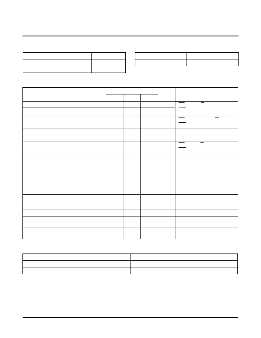
D.C. OPERATING CHARACTERISTICS (Over recommended operating conditions unless otherwise specified.)
7000 FRM T04.1
STANDARD PARTS
7000 FRM T05
Notes: (4) Typical values are for T
A
= 25
∞
C and nominal supply voltage.
(5) This parameter is periodically sampled and not 100% tested.
Symbol
Parameter
Limits
Units
Test Conditions
Min.
Typ.
(4)
Max.
I
CC
V
CC
Active Current (Increment)
50
µ
A
CS = V
IL
, U/D = V
IL
or V
IH
and
INC = 0.4V/2.4V @ max. t
CYC
V
CC
Active Current (Store)
400
µ
A
I
SB
Standby Supply Current
1
µ
A
CS = V
CC
≠ 0.3V, U/D and
INC = V
SS
or V
CC
≠ 0.3V
I
V+
(5)
V
+
Supply Current
400
µ
A
CS = V
IL
, U/D = V
IL
or V
IH
and
INC = 0.4V/2.4V @ max. t
CYC
I
V≠
(5)
V
≠
Supply Current
400
µ
A
CS = V
IL
, U/D = V
IL
or V
IH
and
INC = 0.4V/2.4V @ max. t
CYC
I
LI
CS, INC, U/D Input Leakage
Current
±
10
µ
A
V
IN
= V
SS
to V
CC
V
IH
CS, INC, U/D Input HIGH
Voltage
2
V
CC
+ 1
V
V
IL
CS, INC, U/D Input LOW
Voltage
≠1
0.8
V
R
W
Wiper Resistence
100
200
Max. Wiper Current
±
1mA
V
VH
VH Terminal Voltage
V
≠
V
+
V
V
VL
VL Terminal Voltage
V
≠
V
+
V
V+
Analog Positive Power Supply
V
CC
V
CC
V
V≠
Analog Negative Power
Supply
≠V
CC
0
V
C
IN
(5)
CS, INC, U/D Input
Capacitance
10
pF
V
CC
= 5V, V
IN
= V
SS
, T
A
= 25
∞
C
Part Number
Maximum Resistance
Wiper Increments
Minimum Resistance
X9316Z
1K
32.3
100
X9316W
10K
323
100