 | –≠–ª–µ–∫—Ç—Ä–æ–Ω–Ω—ã–π –∫–æ–º–ø–æ–Ω–µ–Ω—Ç: X9511ZP | –°–∫–∞—á–∞—Ç—å:  PDF PDF  ZIP ZIP |
Document Outline
- Table of Contents
- Product Selection
- Data Sheet Alpha
- Ap Note Alpha
Terminal Voltage
±
5V, 32 Taps
©
Xicor, Inc. 1994, 1995, 1996 Patents Pending
3067-3.5 8/9/97 T2/C0/D0 NS
1
Characteristics subject to change without notice
PushPot
TM
Potentiometer (Push Button Controlled)
FEATURES
∑ Push Button Controlled
∑ Low Power CMOS
--Active Current, 3mA Max
--Standby Current, 200
µ
A Max
∑ 31 Resistive Elements
--Temperature Compensated
--
±
20% End to End Resistance Range
--≠5V to +5V Range
∑ 32 Wiper Tap Points
--Wiper Positioned via Two Push Button Inputs
--Slow & Fast Scan Modes
--AUTOSTORE
Æ
Option
--Manual Store Option
--Wiper Position Stored in Nonvolatile Memory
and Recalled on Power-Up
∑ 100 Year Wiper Position Data Retention
∑ X9511Z = 1K
∑ X9511W = 10K
∑ Packages
--8-Lead PDIP
--8-Lead SOIC
DESCRIPTION
The Xicor X9511 is a push button controlled, potentiom-
eter and is ideal for push button controlled resistance
trimming.
The X9511 is a resistor array composed of 31 resistive
elements. Between each element and at either end are
tap points accessible to the wiper element. The position
of the wiper element is controlled by the PU and PD
inputs. The position of the wiper can be automatically
stored in E
2
memory and then be recalled upon a subse-
quent power-on operation.
The resolution of the X9511 is equal to the maximum
resistance value divided by 31. As an example, for the
X9511W (10K
) each tap point represents 323
.
All Xicor nonvolatile products are designed and tested for
applications requiring extended endurance and data
retention.
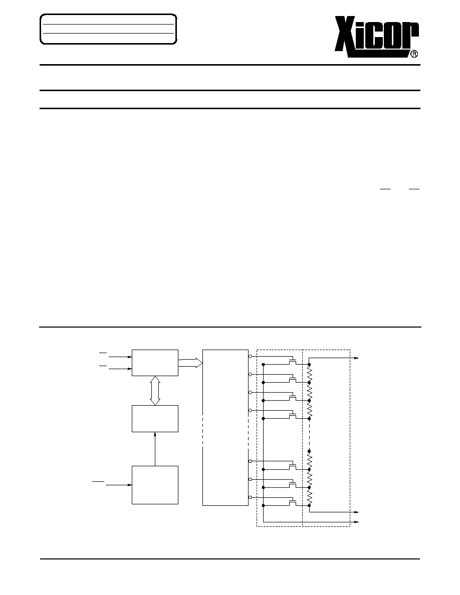
FUNCTIONAL DIAGRAM
3067 ILL F01.1
5-BIT
UP/DOWN
COUNTER
5-BIT
EEPROM
MEMORY
STORE AND
RECALL
CONTROL
CIRCUITRY
ONE
OF
THIRTY-
TWO
DECODER
RESISTOR
ARRAY
31
30
29
28
2
1
0
VL
VW
VH
PU
PD
ASE
TRANSFER
GATES
X9511
AUTOSTORE is a registered trademark of Xicor, Inc.
E
2
POT
TM
and PushPot
TM
are trademarks of Xicor, Inc.
A
PPLICATION
N
OTES
A V A I L A B L E
AN42 ∑ AN44≠48 ∑ AN50 ∑ AN52 ∑ AN53 ∑ AN73
X9511
2
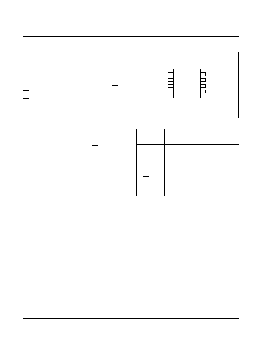
PIN DESCRIPTIONS
V
H
and V
L
The high (V
H
) and low (V
L
) terminals of the X9511 are
equivalent to the fixed terminals of a mechanical potenti-
ometer. The minimum voltage is ≠5V and the maximum
is +5V. It should be noted that the terminology of V
L
and
V
H
references the relative position of the terminal in rela-
tion to wiper movement direction selected by the PU and
PD inputs and not the voltage potential on the terminal.
PU
The debounced PU input is for incrementing the wiper
position. An on-chip pull-up holds the PU input HIGH. A
switch closure to ground or a LOW logic level will, after a
debounce time, move the wiper to the next adjacent
higher tap position.
PD
The debounced PD input is for decrementing the wiper
position. An on-chip pull-up holds the PD input HIGH. A
switch closure to ground or a LOW logic level will, after a
debounce time, move the wiper to the next adjacent
lower tap position.
ASE
The debounced ASE (AUTOSTORE enable) pin can be
in one of two states:
V
IL
≠ Autostore is enabled. When V
CC
powers-down an
automatic store cycle takes place.
V
IH
≠ AUTOSTORE is disabled. A LOW to HIGH will ini-
tiate a manual store operation. This is for a user who
wishes to connect a push button switch to this pin. For
every valid push, the X9511 will store the current wiper
position to the E
2
PROM.
PIN CONFIGURATION
PIN NAMES
3067 FRM T01.1
Symbol
Description
V
H
High Terminal
V
W
Wiper Terminal
V
L
Low Terminal
V
SS
Ground
V
CC
Supply Voltage
PU
Push Up Input
PD
Push Down Input
ASE
AUTOSTORE Enable Input
VCC
ASE
VL
VW
3067 ILL F02.1
PU
PD
VH
VSS
1
2
3
4
8
7
6
5
X9511
DIP/SOIC
X9511
3
DEVICE OPERATION
There are three sections of the X9511: the input control,
counter and decode section; the E
2
PROM memory; and
the resistor array. The input control section operates just
like an up/down counter. The output of this counter is
decoded to turn on a single electronic switch connecting
a point on the resistor array to the wiper output. Under
the proper conditions the contents of the counter can be
stored in E
2
PROM memory and retained for future use.
The resistor array is comprised of 31 individual resistors
connected in series. At either end of the array and
between each resistor is an electronic switch that trans-
fers the potential at that point to the wiper.
The X9511 is designed to interface directly to two push
button switches for effectively moving the wiper up or
down. The PU and PD inputs increment or decrement a
5-bit counter respectively. The output of this counter is
decoded to select one of the thirty-two wiper positions
along the resistive array. The wiper increment input, PU
and the wiper decrement input, PD are both connected
to an internal pull-up so that they normally remain HIGH.
When pulled LOW by an external push button switch or a
logic LOW level input, the wiper will be switched to the
next adjacent tap position.
Internal debounce circuitry prevents inadvertent switch-
ing of the wiper position if PU or PD remain LOW for less
than 40ms, typical. Each of the buttons can be pushed
either once for a single increment/decrement or continu-
ously for a multiple increments/decrements. The number
of increments/decrements of the wiper position depend
on how long the button is being pushed. When making a
continuous push, after the first second, the increment/
decrement speed increases. For the first second the
device will be in the slow scan mode. Then if the button is
held for longer than 1 second the device will go into the
fast scan mode. As soon as the button is released the
X9511 will return to a standby condition.
The wiper, when at either fixed terminal, acts like its
mechanical equivalent and does not move beyond the
last position. That is, the counter does not wrap around
when clocked to either extreme.
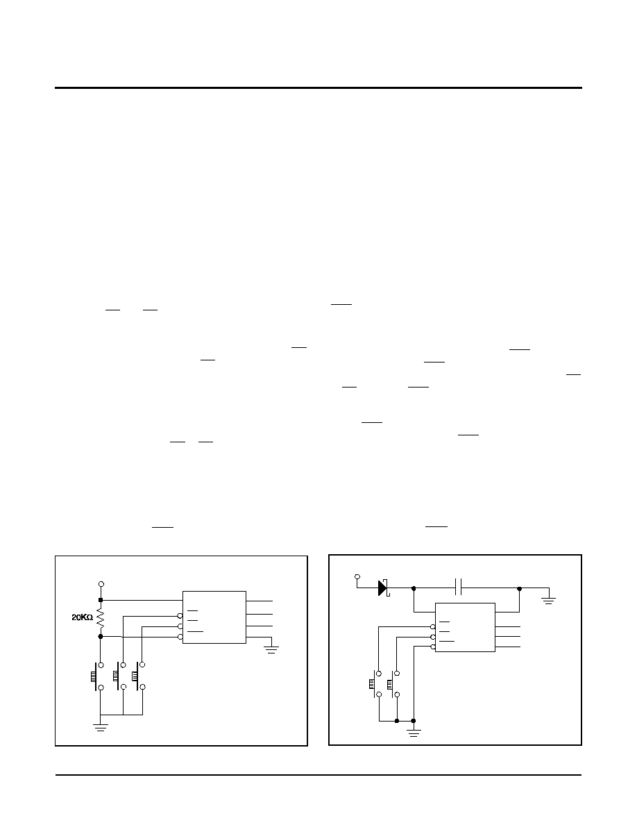
AUTOSTORE
The value of the counter is stored in E
2
PROM memory
whenever the chip senses a power-down of V
CC
while
ASE is enabled (held LOW). When power is restored, the
content of the memory is recalled and the counter reset
to the last value stored.
If AUTOSTORE is to be implemented, ASE is typically
hard wired to V
SS
. If ASE is held HIGH during power-up
and then taken LOW, the wiper will not respond to the PU
or PD inputs until ASE is brought HIGH and held HIGH.
Manual (Push Button) Store
When ASE is not enabled (held HIGH) a push button
switch may be used to pull ASE LOW and released to
perform a manual store of the wiper position.
R
TOTAL
with V
CC
Removed
The end to end resistance of the array will fluctuate once
V
CC
is removed.
Typical circuit with ASE store pin controlled by
push button switch
V
CC
PU
PD
ASE
VH
VW
VL
V
SS
8
1
2
7
3
5
6
3067 ILL F05a
V
CC
Typical circuit with ASE store pin used in
AUTOSTORE mode
V
CC
V
CC
PU
PD
ASE
V
SS
VH
VW
VL
3.3µF
8
1
2
7
4
3
5
6
3067 ILL F05.2
X9511
4
ABSOLUTE MAXIMUM RATINGS*
Temperature under Bias ...................... ≠65
∞
C to +135
∞
C
Storage Temperature........................... ≠65
∞
C to +150
∞
C
Voltage on PU, PD, and V
CC
with Respect to V
SS
................................≠1V to +7V
Voltage on V
H
and V
L
Referenced to V
SS
..................................≠8V to +8V
V = |V
H
≠V
L
|
X9511Z..................................................................4V
X9511W ............................................................ 10V
Lead Temperature (Soldering 10 seconds)...........300
∞
C
Wiper Current
................................................................±
1mA
ANALOG CHARACTERISTICS
Electrical Characteristics
End-to-End Resistance Tolerance
...........................±
20%
Power Rating at 25
∞
C
X9511Z........................................................... 16mW
X9511W ......................................................... 10mW
Wiper Current
.....................................................±
1mA Max.
Typical Wiper Resistance ........................... 40
at 1mA
Typical Noise............................... < ≠120dB/
Hz Ref: 1V
Resolution
Resistance .................................................................3%
Linearity
Absolute Linearity
(1)
...............................................±
1.0 Ml
(2)
Relative Linearity
(3)
.................................................±
0.2 Ml
(2)
*COMMENT
Stresses above those listed under "Absolute Maximum
Ratings" may cause permanent damage to the device.
This is a stress rating only and the functional operation of
the device at these or any other conditions above those
listed in the operational sections of this specification is
not implied. Exposure to absolute maximum rating condi-
tions for extended periods may affect device reliability.
Temperature Coefficient
≠40
∞
C to +85
∞
C
X9511Z...........................................+600 ppm/
∞
C Typical
X9511W .........................................+300 ppm/
∞
C Typical
Ratiometric Temperature Coefficient
................. ±
20 ppm
Wiper Adjustability
Unlimited Wiper Adjustment (Non-Store operation)
Wiper Position Store Operations....................100,000
Data Changes
Physical Characteristics
Marking Includes
Manufacturer's Trademark
Resistance Value or Code
Date Code
Notes:
(1) Absolute Linearity is utilized to determine actual wiper voltage versus expected voltage
= (V
w(n)
(actual) ≠ V
w(n)
(expected)) =
±
1 Ml Maximum.
(2) 1 Ml = Minimum Increment = R
TOT
/31.
(3) Relative Linearity is a measure of the error in step size between taps = V
W(n+1)
≠ [V
w(n)
+ Ml] = +0.2 Ml.
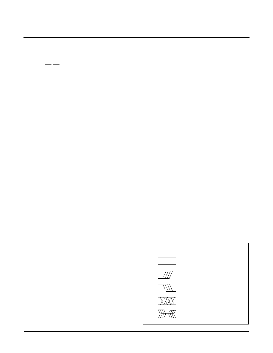
SYMBOL TABLE
WAVEFORM
INPUTS
OUTPUTS
Must be
steady
Will be
steady
May change
from LOW to
HIGH
Will change
from LOW to
HIGH
May change
from HIGH to
LOW
Will change
from HIGH to
LOW
Don't Care:
Changes
Allowed
Changing:
State Not
Known
N/A
Center Line
is High
Impedance
X9511
5
RECOMMENDED OPERATING CONDITIONS
3067 FRM T03
3067 FRM T04.1
Temperature
Min.
Max.
Commercial
0
∞
C
+70
∞
C
Industrial
≠40
∞
C
+85
∞
C
Military
≠55
∞
C
+125
∞
C
Supply Voltage
Limits
X9511
5V
±
10%
D.C. OPERATING CHARACTERISTICS
(Over recommended operating conditions unless otherwise specified.)
3067 FRM T05.4
STANDARD PARTS
3067 FRM T08.1
Notes: (4) Typical values are for T
A
= 25
∞
C and nominal supply voltage.
(5) This parameter is periodically sampled and not 100% tested.
Symbol
Parameter
Limits
Units
Test Conditions
Min.
Typ.
(4)
Max.
I
CC
V
CC
Active Current
1
3
mA
PU or PD held at V
IL
the other at V
IH
I
SB
Standby Supply Current
100
200
µ
A
PU = PD = V
IH
I
LI
PU, PD, ASE Input
Leakage Current
10
µ
A
V
IN
= V
SS
to V
CC
V
IH
PU, PD, ASE Input
HIGH Voltage
2
V
CC
+ 1
V
V
lL
PU, PD, ASE Input
LOW Voltage
≠1
0.8
V
R
W
Wiper Resistance
40
100
Max. Wiper Current
±
1mA
V
VH
VH Terminal Voltage
≠5
+5
V
V
VL
VL Terminal Voltage
≠5
+5
V
C
IN
(5)
ASE, PU, PD Input
Capacitance
10
pF
V
CC
= 5V, V
IN
= 0V,
T
A
= 25
∞
C, f = 1MHz
Part Number
Maximum Resistance
Wiper Increments
Minimum Resistance
X9511Z
1KW
32.3
40
X9511W
10KW
323
40
X9511
6
A.C. OPERATING CHARACTERISTICS (Over recommended operating conditions unless otherwise specified.)
3067 FRM T07.3
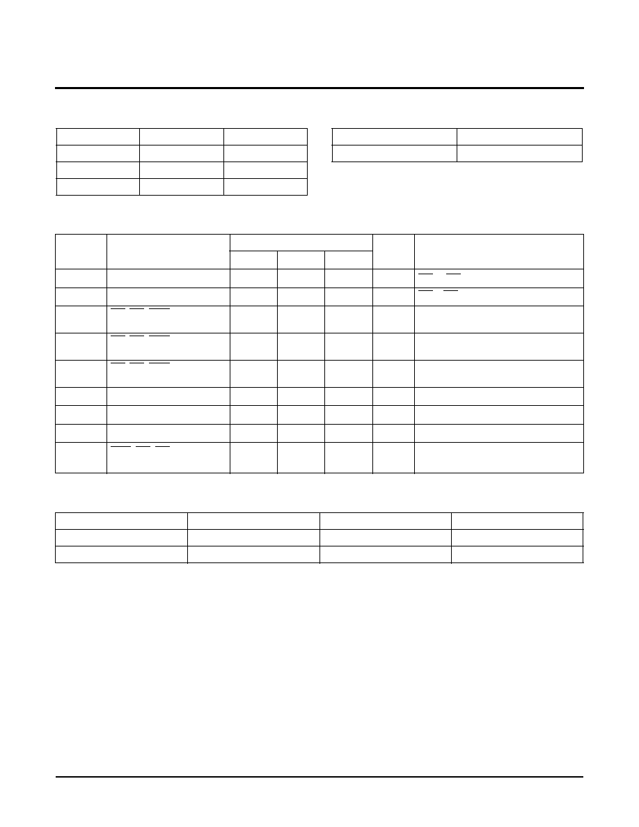
AUTOSTORE Cycle Timing Diagram
Notes: V
ASTH
≠ AUTOSTORE threshold voltage
V
ASEND
≠ AUTOSTORE cycle end voltage
t
ASTO
≠ AUTOSTORE cycle time
(6) Typical values are for T
A
= 25
∞
C and nominal supply voltage.
(7) This parameter is periodically sampled and not 100% tested.
Symbol
Parameter
Limits
Units
Min.
Typ.
(6)
Max.
t
GAP
Time Between Two Separate Push Button Events
0
µ
s
t
DB
Debounce Time
30
60
ms
t
S SLOW
After Debounce to Wiper Change on a Slow Mode
100
250
375
ms
t
S FAST
(7)
Wiper Change on a Fast Mode
25
50
75
ms
t
PU
(7)
Power Up to Wiper Stable
500
µ
s
t
R
V
CC
(7)
V
CC
Power-up Rate
0.2
50
mV/
µ
s
t
ASTO
(7)
AUTOSTORE Cycle Time
2
ms
V
ASTH
(7)
AUTOSTORE Threshold Voltage
4
V
V
ASEND
(7)
AUTOSTORE Cycle End Voltage
3.5
V
3067 ILL F04.2
5
AUTOSTORE CYCLE IN PROGRESS
V
ASTH
V
ASEND
t
ASTO
V
CC
VOL
TS (V)
STORE TIME
TIME (ms)
X9511
7
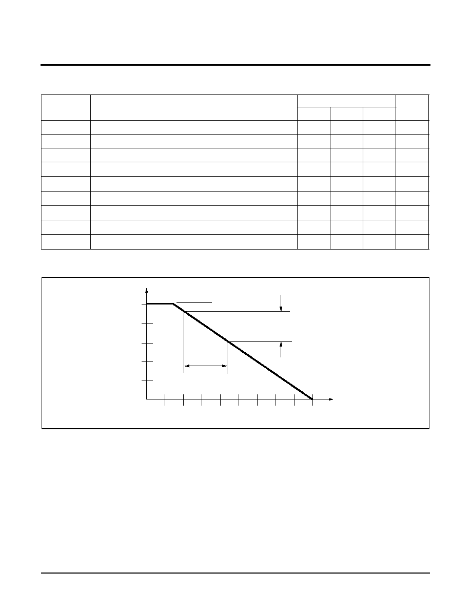
Slow Mode Timing
Notes: (1) MI in the A.C. timing diagram refers to the minimum incremental change in the wiper voltage.
Fast Mode Timing
Notes: (1) MI in the A.C. timing diagram refers to the minimum incremental change in the wiper voltage.
PU
VW
MI
(1)
tDB
3067 ILL F07.1
tGAP
VW
3067 ILL F08
tS SLOW
tS FAST
MI
(1)
1 Second
PU
tDB
X9511
8
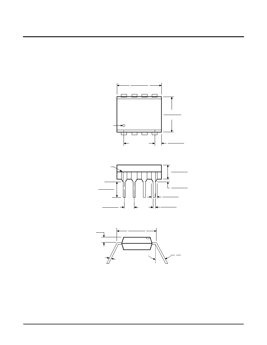
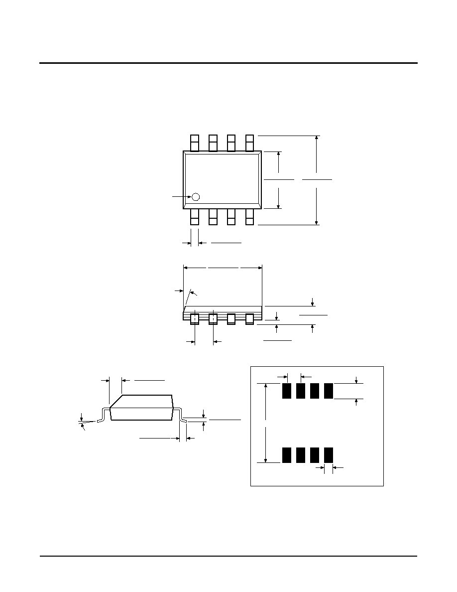
PACKAGING INFORMATION
3926 FHD F01
NOTE:
1. ALL DIMENSIONS IN INCHES (IN PARENTHESES IN MILLIMETERS)
2. PACKAGE DIMENSIONS EXCLUDE MOLDING FLASH
0.020 (0.51)
0.016 (0.41)
0.150 (3.81)
0.125 (3.18)
0.110 (2.79)
0.090 (2.29)
0.430 (10.92)
0.360 (9.14)
0.300
(7.62) REF.
PIN 1 INDEX
0.145 (3.68)
0.128 (3.25)
0.025 (0.64)
0.015 (0.38)
PIN 1
SEATING
PLANE
0.065 (1.65)
0.045 (1.14)
0.260 (6.60)
0.240 (6.10)
0.060 (1.52)
0.020 (0.51)
TYP. 0.010 (0.25)
0
∞
15
∞
8-LEAD PLASTIC DUAL IN-LINE PACKAGE TYPE P
HALF SHOULDER WIDTH ON
ALL END PINS OPTIONAL
0.015 (0.38)
MAX.
0.325 (8.25)
0.300 (7.62)
X9511
9
PACKAGING INFORMATION
0.150 (3.80)
0.158 (4.00)
0.228 (5.80)
0.244 (6.20)
0.014 (0.35)
0.019 (0.49)
PIN 1
PIN 1 INDEX
0.010 (0.25)
0.020 (0.50)
0.050 (1.27)
0.188 (4.78)
0.197 (5.00)
0.004 (0.19)
0.010 (0.25)
0.053 (1.35)
0.069 (1.75)
(4X) 7
∞
0.016 (0.410)
0.037 (0.937)
0.0075 (0.19)
0.010 (0.25)
0
∞
≠ 8
∞
X 45
∞
3926 FHD F22.1
8-LEAD PLASTIC SMALL OUTLINE GULL WING PACKAGE TYPE S
NOTE: ALL DIMENSIONS IN INCHES (IN PARENTHESES IN MILLIMETERS)
0.250"
0.050" TYPICAL
0.050"
TYPICAL
0.030"
TYPICAL
8 PLACES
FOOTPRINT

X9511
10
ORDERING INFORMATION
X9511X
X
X
Temperature Range
Blank = Commercial = 0
∞
C to +70
∞
C
I = Industrial = ≠40
∞
C to +85
∞
C
Package
P = 8-Lead Plastic DIP
LIMITED WARRANTY
Devices sold by Xicor, Inc. are covered by the warranty and patent indemnification provisions appearing in its Terms of Sale only. Xicor, Inc.
makes no warranty, express, statutory, implied, or by description regarding the information set forth herein or regarding the freedom of the
described devices from patent infringement. Xicor, Inc. makes no warranty of merchantability or fitness for any purpose. Xicor, Inc. reserves the
right to discontinue production and change specifications and prices at any time and without notice.
Xicor, Inc. assumes no responsibility for the use of any circuitry other than circuitry embodied in a Xicor, Inc. product. No other circuits, patents,
licenses are implied.
U.S. PATENTS
Xicor products are covered by one or more of the following U.S. Patents: 4,263,664; 4,274,012; 4,300,212; 4,314,265; 4,326,134; 4,393,481;
4,404,475; 4,450,402; 4,486,769; 4,488,060; 4,520,461; 4,533,846; 4,599,706; 4,617,652; 4,668,932; 4,752,912; 4,829, 482; 4,874, 967;
4,883, 976. Foreign patents and additional patents pending.
LIFE RELATED POLICY
In situations where semiconductor component failure may endanger life, system designers using this product should design the system with
appropriate error detection and correction, redundancy and back-up features to prevent such an occurence.
Xicor's products are not authorized for use in critical components in life support devices or systems.
1. Life support devices or systems are devices or systems which, (a) are intended for surgical implant into the body, or (b) support or sustain
life, and whose failure to perform, when properly used in accordance with instructions for use provided in the labeling, can be reasonably
expected to result in a significant injury to the user.
2. A critical component is any component of a life support device or system whose failure to perform can be reasonably expected to cause the
failure of the life support device or system, or to affect its safety or effectiveness.
S = 8-Lead SOIC
M = Military = ≠55
∞
C to +125
∞
C
End to End Resistance
Z = 1K
W = 10K