 | –≠–ª–µ–∫—Ç—Ä–æ–Ω–Ω—ã–π –∫–æ–º–ø–æ–Ω–µ–Ω—Ç: X9C102SI | –°–∫–∞—á–∞—Ç—å:  PDF PDF  ZIP ZIP |
Document Outline
- Table of Contents
- Product Selection
- Data Sheet Alpha
- Ap Note Alpha
X9C102/103/104/503
1
©Xicor, Inc. 1994, 1995 Patents Pending
Characteristics subject to change without notice
3863-2.4 9/18/96 T2/C0/D0 SH
DESCRIPTION
The Xicor X9C102/103/104/503 is a solid state nonvola-
tile potentiometer and is ideal for digitally controlled
resistance trimming.
The X9C102/103/104/503 is a resistor array composed of
99 resistive elements. Between each element and at
either end are tap points accessible to the wiper element.
The position of the wiper element is controlled by the
CS
,
U/
D
, and
INC
inputs. The position of the wiper can be
stored in nonvolatile memory and then be recalled upon a
subsequent power-up operation.
The resolution of the X9C102/103/104/503 is equal to
the maximum resistance value divided by 99. As an
example, for the X9C503 (50K
) each tap point repre-
sents 505
.
All Xicor nonvolatile memories are designed and tested
for applications requiring extended endurance and data
retention.
FEATURES
∑
Compatible with X9102/103/104/503
∑
Low Power CMOS
--V
CC
= 5V
--Active Current, 3mA Max
--Standby Current, 500
µ
A Max
∑
99 Resistive Elements
--Temperature Compensated
--
±
20% End to End Resistance Range
∑
100 Wiper Tap Points
--Wiper Positioned via Three-Wire Interface
--Similar to TTL Up/Down Counter
--Wiper Position Stored in Nonvolatile
Memory and Recalled on Power-Up
∑
100 Year Wiper Position Data Retention
∑
X9C102 = 1K
∑
X9C103 = 10K
∑
X9C503 = 50K
∑
X9C104 = 100K
E
2
POT
TM
Nonvolatile Digital Potentiometer
X9C102/103/104/503
E
2
POT
TM
is a trademark of Xicor, Inc.
3863 FHD F01
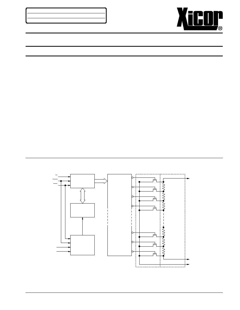
FUNCTIONAL DIAGRAM
7-BIT
UP/DOWN
COUNTER
7-BIT
NONVOLATILE
MEMORY
STORE AND
RECALL
CONTROL
CIRCUITRY
ONE
OF
ONE-
HUNDRED
DECODER
RESISTOR
ARRAY
99
98
97
96
2
1
0
VL
VW
VH
U/D
INC
CS
VCC
GND
TRANSFER
GATES
Terminal Voltage
±
5V, 100 Taps
A
PPLICATION
N
OTES
A V A I L A B L E
AN42 ∑ AN44≠48 ∑ AN50 ∑ AN52 ∑ AN53 ∑ AN71 ∑ AN73
X9C102/103/104/503
2
PIN DESCRIPTIONS
V
H
and V
L
The high (V
H
) and low (V
L
) terminals of the X9C102/103/
104/503 are equivalent to the fixed terminals of a
mechanical potentiometer. The minimum voltage is ≠5V
and the maximum is +5V. It should be noted that the
terminology of V
L
and V
H
references the relative position
of the terminal in relation to wiper movement direction
selected by the U/
D
input and not the voltage potential on
the terminal.
V
W
V
W
is the wiper terminal, equivalent to the movable
terminal of a mechanical potentiometer. The position
of the wiper within the array is determined by the
control inputs. The wiper terminal series resistance is
typically 40
.
Up/Down (U/
D
)
The U/
D
input controls the direction of the wiper
movement and whether the counter is incremented or
decremented.
Increment (
INC
)
The
INC
input is negative-edge triggered. Toggling
INC
will move the wiper and either increment or decrement
the counter in the direction indicated by the logic level on
the U/
D
input.
Chip Select (
CS
)
The device is selected when the
CS
input is LOW. The
current counter value is stored in nonvolatile memory
when
CS
is returned HIGH while the
INC
input is also
HIGH. After the store operation is complete the X9C102/
103/104/503 will be placed in the low power standby
mode until the device is selected once again.
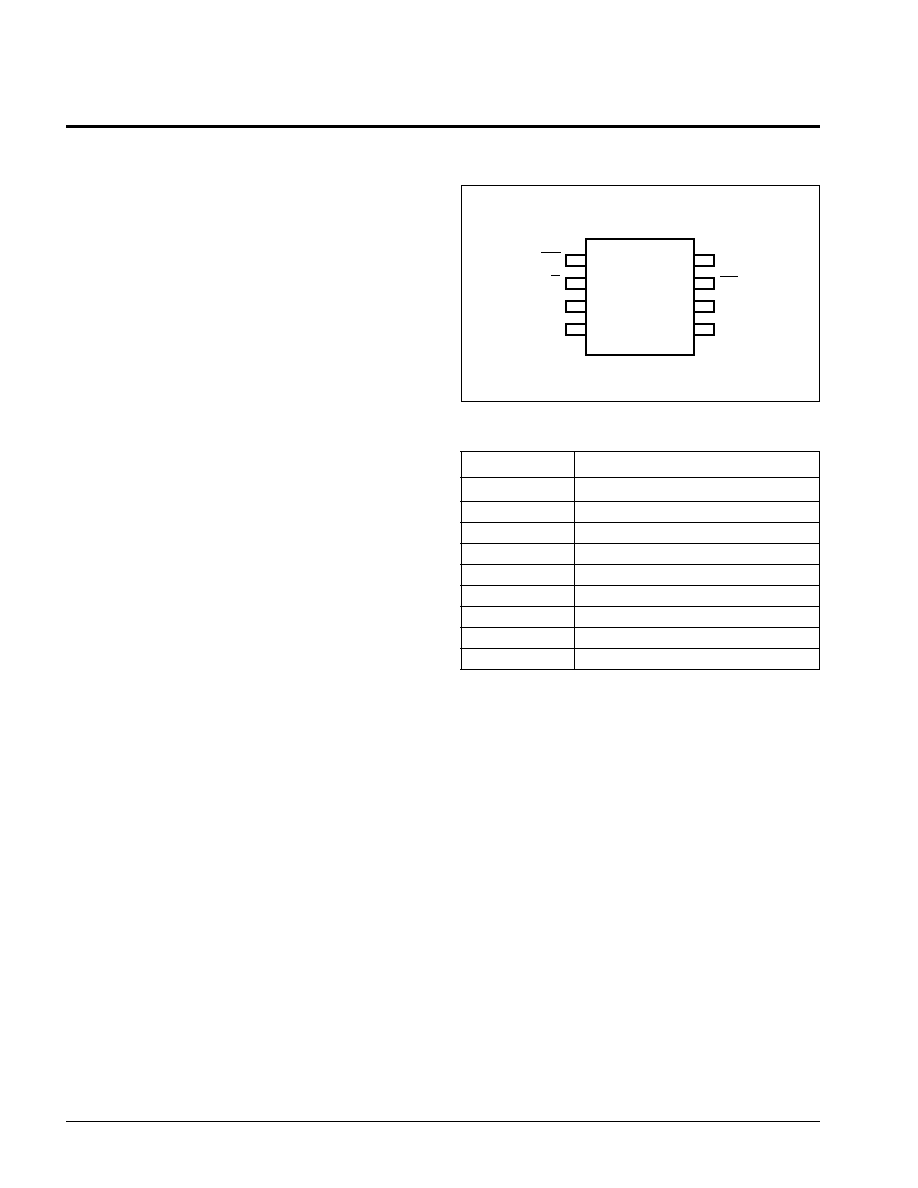
PIN CONFIGURATION
PIN NAMES
Symbol
Description
V
H
High Terminal
V
W
Wiper Terminal
V
L
Low Terminal
V
SS
Ground
V
CC
Supply Voltage
U/
D
Up/Down Input
INC
Increment Input
CS
Chip Select Input
NC
No Connect
3863 PGM T01
VCC
CS
VL
VW
3863 FHD F02.2
INC
U/D
VH
VSS
1
2
3
4
8
7
6
5
X9C102/
103/104/503
DIP/SOIC
X9C102/103/104/503
3
DEVICE OPERATION
There are three sections of the X9C102/103/104/503:
the input control, counter and decode section; the non-
volatile memory; and the resistor array. The input control
section operates just like an up/down counter. The
output of this counter is decoded to turn on a single
electronic switch connecting a point on the resistor array
to the wiper output. Under the proper conditions the
contents of the counter can be stored in nonvolatile
memory and retained for future use. The resistor array
is comprised of 99 individual resistors connected in
series. At either end of the array and between each
resistor is an electronic switch that transfers the
potential at that point to the wiper.
The
INC
, U/
D
and
CS
inputs control the movement of the
wiper along the resistor array. With
CS
set LOW the
X9C102/103/104/503 is selected and enabled to
respond to the U/
D
and
INC
inputs. HIGH to LOW
transitions on
INC
will increment or decrement
(depending on the state of the U/
D
input) a seven-bit
counter. The output of this counter is decoded to
select one of one-hundred wiper positions along the
resistive array.
The wiper, when at either fixed terminal, acts like its
mechanical equivalent and does not move beyond the
last position. That is, the counter does not wrap around
when clocked to either extreme.
The value of the counter is stored in nonvolatile memory
whenever
CS
transistions HIGH while the
INC
input is
also HIGH.
When the X9C102/103/104/503 is powered-down, the
last counter position stored will be maintained in the
nonvolatile memory. When power is restored, the con-
tents of the memory are recalled and the counter is reset
to the value last stored.
OPERATION NOTES
The system may select the X9C102/103/104/503, move
the wiper, and deselect the device without having to
store the latest wiper, position in nonvolatile memory.
The wiper movement is performed as described above;
once the new position is reached, the system would the
keep
INC
LOW while taking
CS
HIGH. The new wiper
position would be maintained until changed by the
system or until a power-down/up cycle recalled the
previously stored data.
This would allow the system to always power-up to a
preset value stored in nonvolatile memory; then during
system operation minor adjustments could be made.
The adjustments might be based on user preference:
system parameter changes due to temperature drift,
etc...
The state of U/
D
may be changed while
CS
remains
LOW. This allows the host system to enable the
X9C102/103/104/503 and then move the wiper up and
down until the proper trim is attained.
T
IW
/R
TOTAL
The electronic switches on the X9C102/103/104/503
operate in a "make before break" mode when the wiper
changes tap positions. If the wiper is moved several
positions, multiple taps are connected to the wiper for
t
IW
(
INC
to V
W
change). The R
TOTAL
value for the device
can temporarily be reduced by a significant amount
if the wiper is moved several positions.
R
TOTAL
with V
CC
Removed
The end to end resistance of the array will fluctuate once
V
CC
is removed.
SYMBOL TABLE
WAVEFORM
INPUTS
OUTPUTS
Must be
steady
Will be
steady
May change
from LOW
to HIGH
Will change
from LOW
to HIGH
May change
from HIGH
to LOW
Will change
from HIGH
to LOW
Don't Care:
Changes
Allowed
Changing:
State Not
Known
N/A
Center Line
is High
Impedance
X9C102/103/104/503
4
ABSOLUTE MAXIMUM RATINGS*
Temperature under Bias .................. ≠65
∞
C to +135
∞
C
Storage Temperature ....................... ≠65
∞
C to +150
∞
C
Voltage on
CS
,
INC
, U/
D
and V
CC
with Respect to V
SS ...............................
≠1V to +7V
Voltage on V
H
and V
L
Referenced to V
SS .................................
≠8V to +8V
V = |V
H
≠V
L
|
X9C102 ............................................................. 4V
X9C103, X9C503, and X9C104 ...................... 10V
Lead Temperature (Soldering, 10 seconds) .... +300
∞
C
Wiper Current .....................................................
±
1mA
*COMMENT
Stresses above those listed under "Absolute Maximum
Ratings" may cause permanent damage to the device.
This is a stress rating only and the functional operation
of the device at these or any other conditions above
those listed in the operational sections of this specifica-
tion is not implied. Exposure to absolute maximum
rating conditions for extended periods may affect device
reliability.
ANALOG CHARACTERISTICS
Electrical Characteristics
End-to-End Resistance Tolerance .....................
±
20%
Power Rating at 25
∞
C
X9C102 ....................................................... 16mW
X9C103, X9C503, and X9C104 .................. 10mW
Wiper Current ............................................
±
1mA Max.
Typical Wiper Resistance ......................... 40
at 1mA
Typical Noise .......................... < ≠120dB/
Hz Ref: 1V
Resolution
Resistance ............................................................. 1%
Linearity
Absolute Linearity
(1) ........................................
±
1.0 Ml
(2)
Relative Linearity
(3)
.....................................
±
0.2 Ml
(2)
Temperature Coefficient
(≠40
∞
C to +85
∞
C)
X9C102 ...................................... +600 ppm/
∞
C Typical
X9C103, X9C503, X9C104 ........ +300 ppm/
∞
C Typical
Ratiometric Temperature Coefficient ............
±
20 ppm
Wiper Adjustability
Unlimited Wiper Adjustment (Non-Store operation)
Wiper Position Store Operations ................... 10,000
Data Changes
Physical Characteristics
Marking Includes
Manufacturer`s Trademark
Resistance Value or Code
Date Code
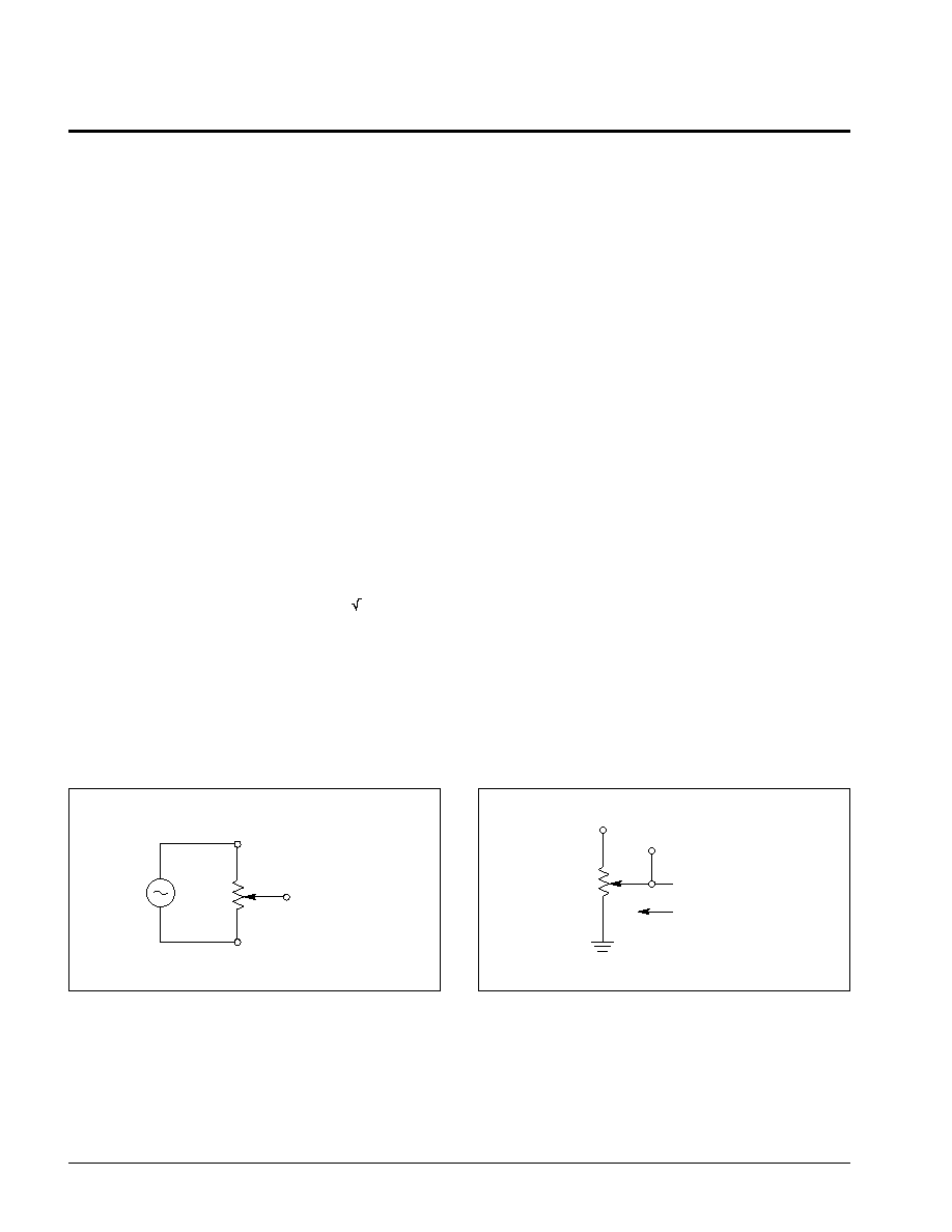
Test Circuit #1
Test Circuit #2
3863 FHD F04
3863 FHD F05
FORCE
CURRENT
VL
VW
VH
TEST POINT
TEST POINT
VW
VH
VL
Notes: (1) Absolute Linearity is utilized to determine actual wiper voltage versus expected voltage
= (V
w(n)
(actual) ≠ V
w(n)
(expected)) =
±
1 Ml Maximum.
(2) 1 Ml = Minimum Increment = R
TOT
/99.
(3) Relative Linearity is a measure of the error in step size between taps = V
W(n+1)
≠ [V
w(n)
+ Ml] = +0.2 Ml.
X9C102/103/104/503
5
RECOMMENDED OPERATING CONDITIONS
Temperature
Min.
Max.
Commercial
0
∞
C
+70
∞
C
Industrial
≠40
∞
C
+85
∞
C
Military
≠55
∞
C
+125
∞
C
3863 PGM T03.1
Supply Voltage
Limits
X9C102/103/104/503
5V
±
10%
D.C. OPERATING CHARACTERISTICS (Over recommended operating conditions unless otherwise specified.)
Limits
Symbol
Parameter
Min.
Typ.
(4)
Max.
Units
Test Conditions
I
CC
V
CC
Active Current
1
3
mA
CS
= V
IL
, U/
D
= V
IL
or V
IH
and
INC
= 0.4V to 2.4V @ max. t
CYC
I
SB
Standby Supply Current
200
500
µ
A
CS
= V
CC
≠ 0.3V, U/
D
and
INC
=
V
SS
or V
CC
≠ 0.3V
I
LI
CS
,
INC
, U/
D
Input
±
10
µ
A
V
IN
= V
SS
to V
CC
Leakage Current
V
IH
CS
,
INC
, U/
D
Input
2
V
CC
+ 1
V
HIGH Voltage
V
IL
CS
,
INC
, U/
D
Input
≠1
0.8
V
LOW Voltage
R
W
Wiper Resistence
40
100
Max. Wiper Current
±
1mA
V
H
VH Terminal Voltage
≠5
+5
V
V
L
VL Terminal Voltage
≠5
+5
V
C
IN
(5)
CS
,
INC
, U/
D
Input
10
pF
V
CC
= 5V, V
IN
= V
SS
,
Capacitance
T
A
= 25
∞
C, f = 1MHz
3863 PGM T05.3
STANDARD PARTS
Part Number
Maximum Resistance
Wiper Increments
Minimum Resistance
X9C102
1K
10.1
40
X9C103
10K
101
40
X9C503
50K
505
40
X9C104
100K
1010
40
3863 PGM T08.1
Notes: (4) Typical values are for T
A
= 25
∞
C and nominal supply voltage.
(5) This parameter is periodically sampled and not 100% tested.
3863 PGM T04.2
X9C102/103/104/503
6
A.C. CONDITIONS OF TEST
Input Pulse Levels
0V to 3V
Input Rise and Fall Times
10ns
Input Reference Levels
1.5V
3863 PGM T05.1
MODE SELECTION
CS
INC
U/
D
Mode
L
H
Wiper Up
L
L
Wiper Down
H
X
Store Wiper Position
H
X
X
Standby Current
L
X
No Store, Return to
Standby
3863 PGM T06
A.C. OPERATING CHARACTERISTICS (Over recommended operating conditions unless otherwise specified)
Limits
Symbol
Parameter
Min.
Typ.
(6)
Max.
Units
t
Cl
CS
to
INC
Setup
100
ns
t
lD
INC
HIGH to U/
D
Change
100
ns
t
DI
U/
D
to
INC
Setup
2.9
µ
s
t
lL
INC
LOW Period
1
µ
s
t
lH
INC
HIGH Period
1
µ
s
t
lC
INC
Inactive to
CS
Inactive
1
µ
s
t
CPH
CS
Deselect Time
20
ms
t
IW
INC
to Vw Change
100
500
µ
s
t
CYC
INC
Cycle Time
4
µ
s
t
R,
t
F
(7)
INC
Input Rise and Fall Time
500
µ
s
t
PU
(7)
Power up to Wiper Stable
500
µ
s
t
R
V
CC
(7)
V
CC
Power-up Rate
0.2
50
mV/
µ
s
3863 PGM T07.3
A.C. Timing
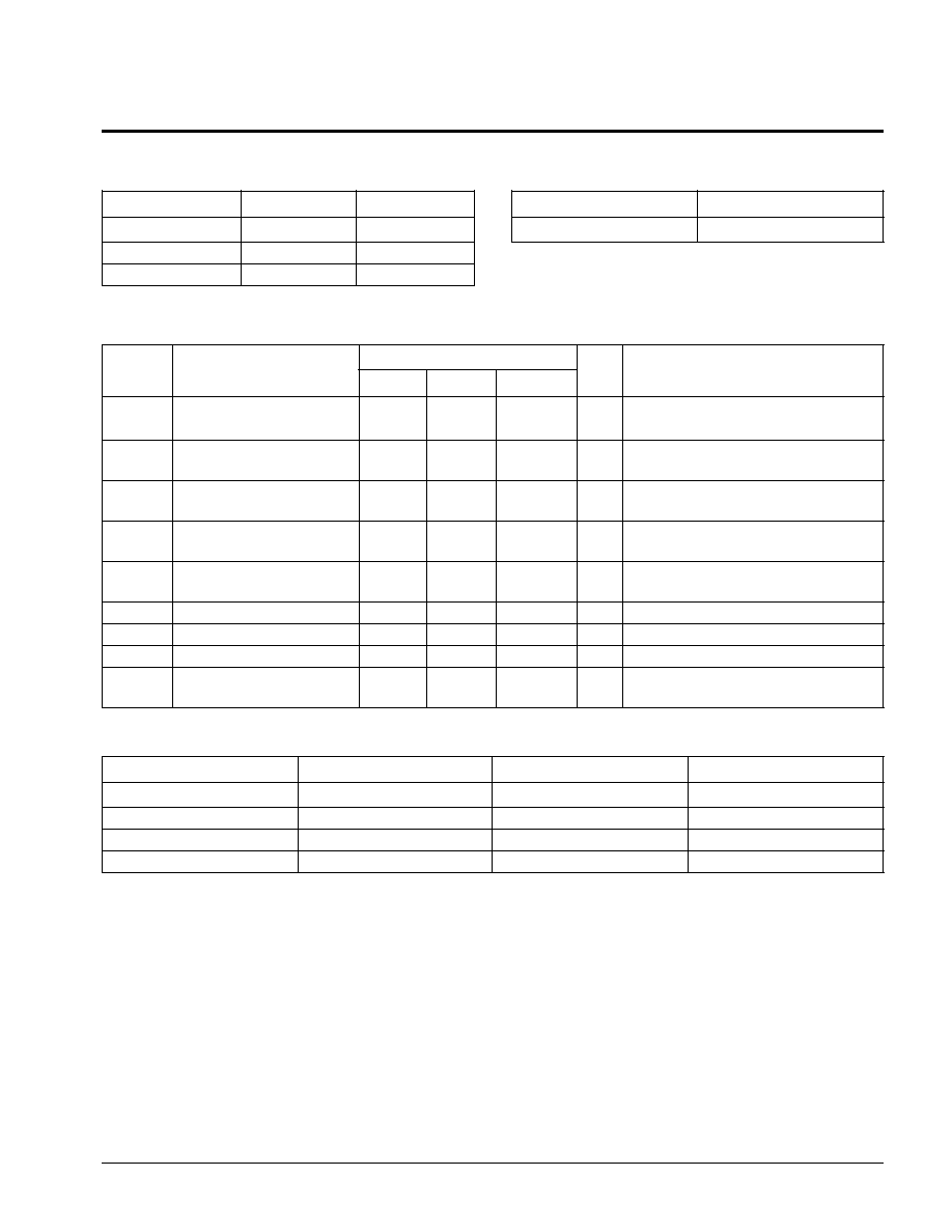
3863 FHD F03
CS
INC
U/D
VW
tCI
tIL
tIH
tCYC
tID
tDI
tIW
MI
(8)
tIC
tCPH
tF
tR
10%
90%
90%
Notes: (6) Typical values are for T
A
= 25
∞
C and nominal supply voltage.
(7) This parameter is periodically sampled and not 100% tested.
(8) MI in the A.C. timing diagram refers to the minimum incremental change in the V
W
output due to a change in the wiper position.
X9C102/103/104/503
7
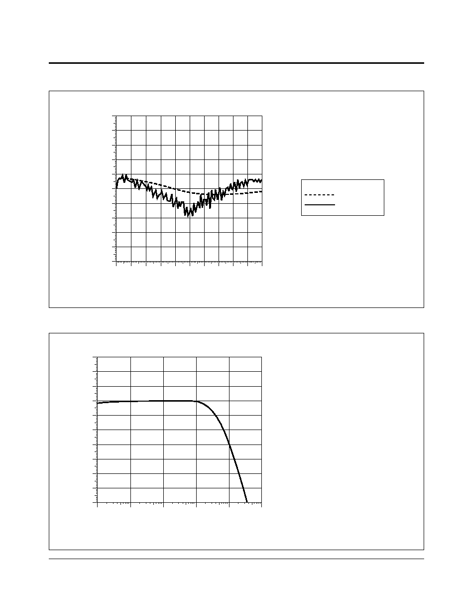
Typical Frequency Response for X9C102
TEST CONDITIONS
V
CC
= 5V
Temp. = 25
∞
C
Wiper @ Tap 50
V
H
= 0.5V
RMS
Normalized (0dB @ 1KHz)
Test Circuit #1
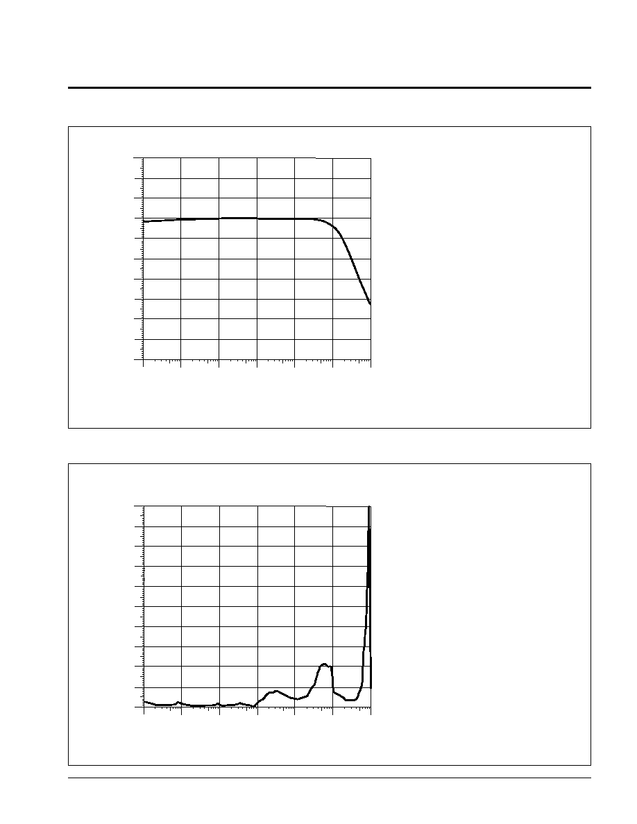
TEST CONDITIONS
V
CC
= 5V
Temp. = 25
∞
C
Wiper @ Tap 50
V
H
= 2V
RMS
Test Circuit #1
Typical Total Harmonic Distortion for X9C102
NORMALIZED GAIN (dB)
9
6
3
0
≠3
≠6
≠9
≠12
≠15
≠18
≠21
0.01
0.10
1.00
10.00
100.00 1000.00 10000.00
FREQUENCY IN KHz
THD (%)
2.0
1.8
1.6
1.4
1.2
1.0
0.8
0.6
0.4
0.2
0.0
0.01
0.10
1.00
10.00
100.00 1000.00 10000.00
FREQUENCY IN KHz
3863 FHD F06
3863 FHD F07
X9C102/103/104/503
8
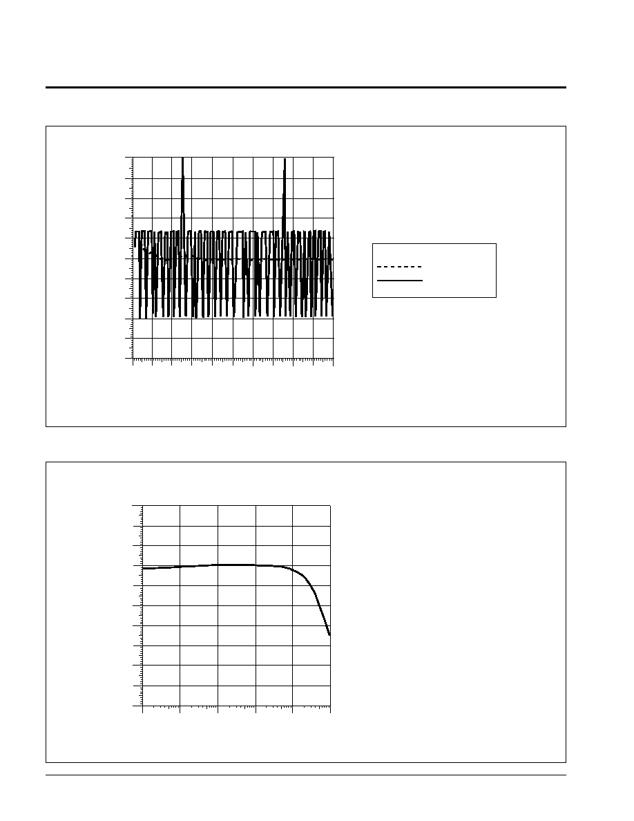
Typical Linearity for X9C102
Typical Frequency Response for X9C103
TEST CONDITIONS
V
CC
= 5V
Temp. = 25
∞
C
Test Circuit #2
TEST CONDITIONS
V
CC
= 5V
Temp. = 25
∞
C
Wiper @ Tap 50
V
H
= 0.5V
RMS
Normalized (0dB @ 1KHz)
Test Circuit #1
PERCENTAGE ERROR
0
WIPER POSITION
10
20
30
40
50
60
70
80
90 100
10
8
6
4
2
0
≠2
≠4
≠6
≠8
≠10
KEY:
= RELATIVE
= ABSOLUTE
0039≠9
NORMALIZED GAIN (dB)
9
6
3
0
≠3
≠6
≠9
≠12
≠15
≠18
≠21
0.01
0.10
1.00
10.00
100.00 1000.00
FREQUENCY IN KHz
3863 FHD F08
3863 FHD F09

X9C102/103/104/503
9
Typical Total Harmonic Distortion for X9C103
Typical Linearity for X9C103
TEST CONDITIONS
V
CC
= 5V
Temp. = 25
∞
C
Test Circuit #2
TEST CONDITIONS
V
CC
= 5V
Temp. = 25
∞
C
Wiper @ Tap 50
V
H
= 2V
RMS
Test Circuit #1
THD (%)
2.0
1.8
1.6
1.4
1.2
1.0
0.8
0.6
0.4
0.2
0.0
0.01
0.10
1.00
10.00
100.00 1000.00
FREQUENCY IN KHz
PERCENTAGE ERROR
0
WIPER POSITION
10
20
30
40
50
60
70
80
90 100
10
8
6
4
2
0
≠2
≠4
≠6
≠8
≠10
KEY:
= RELATIVE
= ABSOLUTE
0039≠9
3863 FHD F10
3863 FHD F11

X9C102/103/104/503
10
Typical Frequency Response for X9C503
Typical Total Harmonic Distortion for X9C503
TEST CONDITIONS
V
CC
= 5V
Temp. = 25
∞
C
Wiper @ Tap 50
V
H
= 2V
RMS
Test Circuit #1
TEST CONDITIONS
V
CC
= 5V
Temp. = 25
∞
C
Wiper @ Tap 50
V
H
= 0.5V
RMS
Normalized (0dB @ 1 KHz)
Test Circuit #1
9
6
3
0
-3
-6
-9
-12
-15
-18
-21
0.01
0.10
1.00
10.00
100.00
FREQUENCY IN KHz
NORMALIZED GAIN (dB)
1000.00
9
1.8
1.6
1.4
1.2
1.0
0.8
0.6
0.4
0.2
0.0
0.01
0.10
1.00
10.00
100.00
FREQUENCY IN KHz
THD (%)
1000.00
3863 FHD F12
3863 FHD F13
X9C102/103/104/503
11
Typical Linearity for X9C503
Typical Frequency Response for X9C104
TEST CONDITIONS
V
CC
= 5V
Temp. = 25
∞
C
Wiper @ Tap 50
V
H
= 0.5V
RMS
Normalized (0dB @ 1 KHz)
Test Circuit #1
TEST CONDITIONS
V
CC
= 5V
Temp. = 25
∞
C
Test Circuit #2
10
8
6
4
2
0
-2
-4
-6
-8
-10
0
10
20
30
40
50
60
70
80
90 100
WIPER POSITION
PERCENTAGE ERROR
9
6
3
0
-3
-6
-9
-12
-15
-18
-21
0.01
0.10
1.00
10.00
100.00
1000.00
FREQUENCY IN KHz
NORMALIZED GAIN (dB)
KEY:
= RELATIVE
= ABSOLUTE
0039≠9
3863 FHD F14
3863 FHD F15
X9C102/103/104/503
12
Typical Total Harmonic Distortion for X9C104
Typical Linearity for X9C104
TEST CONDITIONS
V
CC
= 5V
Temp. = 25
∞
C
Wiper @ Tap 50
V
H
= 2V
RMS
Test Circuit #1
TEST CONDITIONS
V
CC
= 5V
Temp. = 25
∞
C
Test Circuit #2
2.0
1.8
1.6
1.4
1.2
1.0
0.8
0.6
0.4
0.2
0.0
0.01
0.10
1.00
10.00
100.00
10000.00
FREQUENCY IN KHz
THD (%)
1000.00
10
8
6
4
2
0
-2
-4
-6
-8
-10
0
10
20
30
40
50
60
70
80
90 100
WIPER POSITION
PERCENTAGE ERROR
KEY:
= RELATIVE
= ABSOLUTE
0039≠9
3863 FHD F16
3863 FHD F17
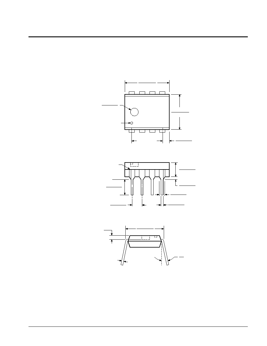
X9C102/103/104/503
13
0.020 (0.51)
0.016 (0.41)
0.150 (3.81)
0.125 (3.18)
0.325 (8.25)
0.300 (7.62)
0.110 (2.79)
0.090 (2.29)
0.430 (10.92)
0.360 (9.14)
0.300
(7.62) REF.
PIN 1 INDEX
0.140 (3.56)
0.130 (3.30)
0.020 (0.51)
0.015 (0.38)
3926 FHD F01
PIN 1
SEATING
PLANE
0.062 (1.57)
0.058 (1.47)
0.255 (6.47)
0.245 (6.22)
0.060 (1.52)
0.020 (0.51)
TYP. 0.010 (0.25)
0
∞
15
∞
NOTE: ALL DIMENSIONS IN INCHES (IN PARENTHESES IN MILLIMETERS)
0.092 (2.34)
DIA. NOM.
HALF SHOULDER WIDTH ON
ALL END PINS OPTIONAL
0.015 (0.38)
MAX.
PACKAGING INFORMATION
8-LEAD PLASTIC DUAL IN-LINE PACKAGE TYPE P
NOTE: ALL DIMENSIONS IN INCHES (IN PARENTHESES IN MILLIMETERS)
X9C102/103/104/503
14
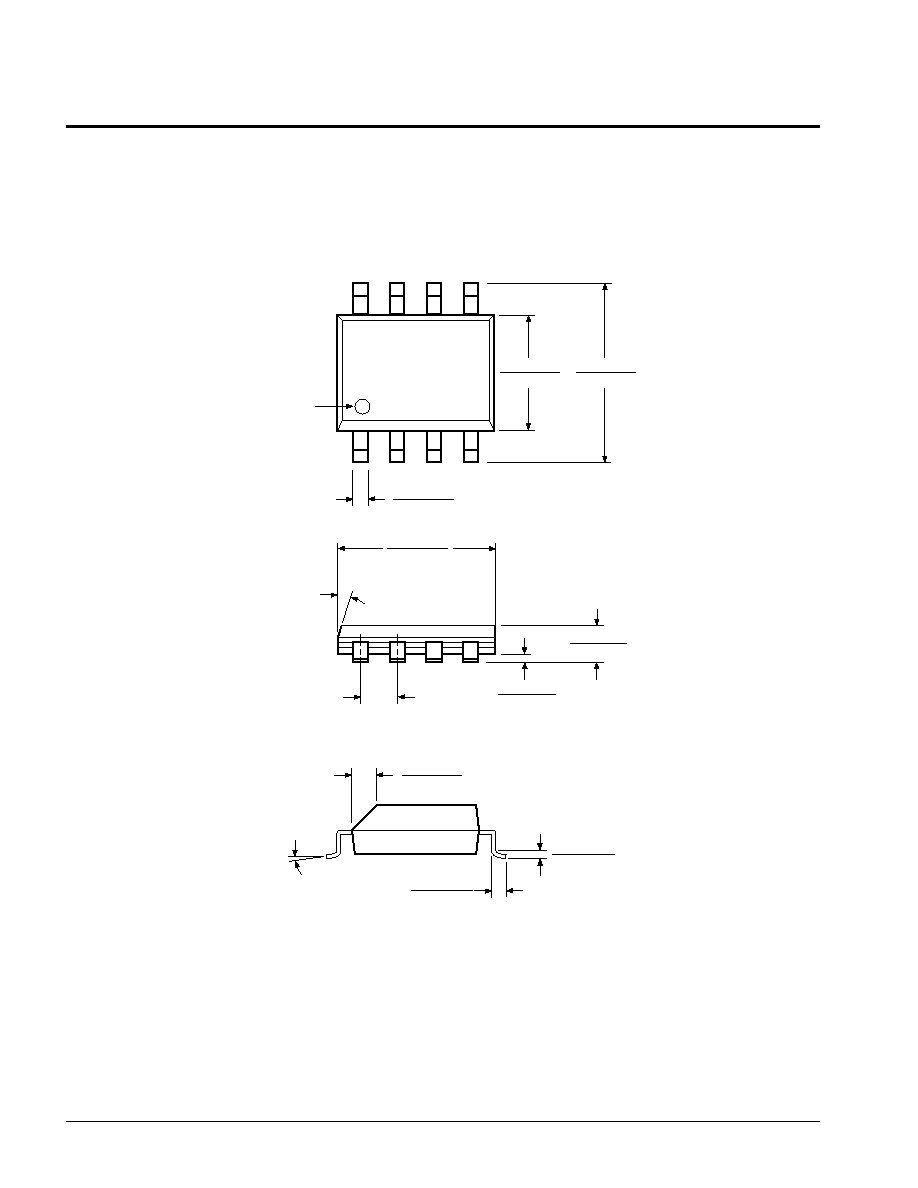
PACKAGING INFORMATION
0.150 (3.80)
0.158 (4.00)
0.228 (5.80)
0.244 (6.20)
0.014 (0.35)
0.019 (0.49)
PIN 1
PIN 1 INDEX
0.010 (0.25)
0.020 (0.50)
0.050 (1.27)
0.188 (4.78)
0.197 (5.00)
0.004 (0.19)
0.010 (0.25)
0.053 (1.35)
0.069 (1.75)
(4X) 7
∞
0.027 (0.683)
0.037 (0.937)
0.0075 (0.19)
0.010 (0.25)
0
∞
≠ 8
∞
X 45
∞
3926 FHD F22
8-LEAD PLASTIC SMALL OUTLINE GULL WING PACKAGE TYPE S
NOTE: ALL DIMENSIONS IN INCHES (IN PARENTHESIS IN MILLIMETERS)
X9C102/103/104/503
15
LIMITED WARRANTY
Devices sold by Xicor, Inc. are covered by the warranty and patent indemnification provisions appearing in its Terms of Sale only. Xicor, Inc. makes no warranty,
express, statutory, implied, or by description regarding the information set forth herein or regarding the freedom of the described devices from patent infringement.
Xicor, Inc. makes no warranty of merchantability or fitness for any purpose. Xicor, Inc. reserves the right to discontinue production and change specifications and
prices at any time and without notice.
Xicor, Inc. assumes no responsibility for the use of any circuitry other than circuitry embodied in a Xicor, Inc. product. No other circuits, patents, licenses are
implied.
U.S. PATENTS
Xicor products are covered by one or more of the following U.S. Patents: 4,263,664; 4,274,012; 4,300,212; 4,314,265; 4,326,134; 4,393,481; 4,404,475;
4,450,402; 4,486,769; 4,488,060; 4,520,461; 4,533,846; 4,599,706; 4,617,652; 4,668,932; 4,752,912; 4,829, 482; 4,874, 967; 4,883, 976. Foreign patents and
additional patents pending.
LIFE RELATED POLICY
In situations where semiconductor component failure may endanger life, system designers using this product should design the system with appropriate error
detection and correction, redundancy and back-up features to prevent such an occurence.
Xicor's products are not authorized for use in critical components in life support devices or systems.
1. Life support devices or systems are devices or systems which, (a) are intended for surgical implant into the body, or (b) support or sustain life, and whose
failure to perform, when properly used in accordance with instructions for use provided in the labeling, can be reasonably expected to result in a significant
injury to the user.
2. A critical component is any component of a life support device or system whose failure to perform can be reasonably expected to cause the failure of the life
support device or system, or to affect its safety or effectiveness.
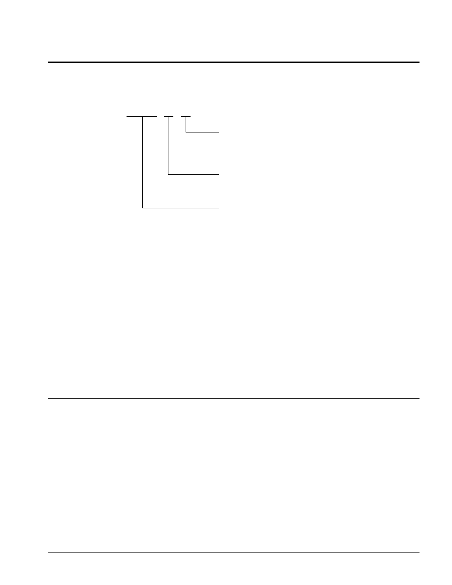
Temperature Range
Blank = Commercial = 0
∞
C to +70
∞
C
I = Industrial = ≠40
∞
C to +85
∞
C
M = Military = ≠55
∞
C to +125
∞
C
Package
P = 8-Lead Plastic DIP
S = 8-Lead SOIC
End to End Resistance
102 = 1K
103 = 10K
503 = 50K
104 = 100K
X9CXXX
X
X
ORDERING INFORMATION