 | –≠–ª–µ–∫—Ç—Ä–æ–Ω–Ω—ã–π –∫–æ–º–ø–æ–Ω–µ–Ω—Ç: X9C303 | –°–∫–∞—á–∞—Ç—å:  PDF PDF  ZIP ZIP |
REV 1.1 4/27/01
Characteristics subject to change without notice.
1 of 10
www.xicor.com
XDCP
TM
is a trademark of Xicor, Inc.
FEATURES
∑ Solid-state potentiometer
∑ Three-wire serial interface
∑ 100 wiper tap points
--Wiper position stored in nonvolatile memory
and recalled on power-up
∑ 99 resistive elements, log taper
--Temperature compensated
--End to end resistance, ±15%
--Terminal voltages, ±5V
∑ Low power CMOS
--V
CC
= 5V
--Active current, 3mA max.
--Standby current, 750µA max.
∑ High reliability
--Endurance, 100,000 data changes per bit
--Register data retention, 100 years
∑ X9C303, 32 k
∑ Packages
--8-lead TSSOP
--8-lead SOIC
--8-pin DIP
DESCRIPTION
The Xicor X9C303 is a digitally controlled potentiome-
ter (XDCP). The device consists of a resistor array,
wiper switches, a control section, and nonvolatile
memory. The wiper position is controlled by a three-
wire interface.
The resistor array is composed of 99 resistive ele-
ments. Between each element and at either end are
tap points accessible to the wiper terminal. The posi-
tion of the wiper element is controlled by the CS, U/D,
and INC inputs. The position of the wiper can be
stored in nonvolatile memory and then be recalled
upon a subsequent power-up operation.
The device can be used as a three-terminal potentio-
meter or as a two-terminal variable resistor in a wide
variety of applications ranging from control, to signal
processing, to parameter adjustment. Digitally-
controlled potentiometers provide three powerful appli-
cation advantages; (1) the variability and reliability of a
solid-state potentiometer, (2) the flexibility of com-
puter-based digital controls, and (3) the use of nonvol-
atile memory for potentiometer settings retention.
X9C303
Digitally Controlled Potentiometer (XDCP
TM
)
A
PPLICATION
N
OTE
A V A I L A B L E
AN42 ∑ AN44≠48 ∑ AN50 ∑ AN52 ∑ AN53 ∑ AN71 ∑ AN92
Terminal Voltage ±5V, 100 Taps, Log Taper
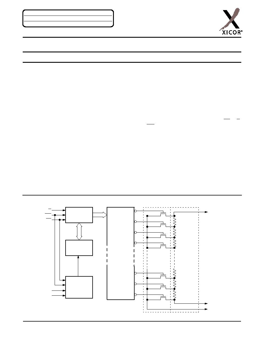
BLOCK DIAGRAM
7-Bit
Up/Down
Counter
7-Bit
Nonvolatile
Memory
Store and
Recall
Control
Circuitry
One
of
Hundred
Decoder
Resistor
Array
R
L/
V
L
R
W/
V
W
R
H/
V
H
U/D
INC
CS
Transfer
V
CC
One-
Gates
99
98
97
96
2
1
0
V
SS

X9C303
Characteristics subject to change without notice.
2 of 10
REV 1.1 4/27/01
www.xicor.com
PIN DESCRIPTIONS
V
H
and V
L
The high (V
H
) and low (V
L
) terminals of the device are
equivalent to the fixed terminals of a mechanical
potentiometer. The minimum voltage is ≠5V and the
maximum is +5V. It should be noted that the terminol-
ogy of V
L
and V
H
references the relative position of the
terminal in relation to wiper movement direction
selected by the U/D input and not the voltage potential
on the terminal.
V
W
V
W
is the wiper terminal, equivalent to the movable ter-
minal of a mechanical potentiometer. The position of
the wiper within the array is determined by the control
inputs. The wiper terminal series resistance is typically
40
.
Up/Down (U/D)
The U/D input controls the direction of the wiper move-
ment and whether the counter is incriminated or decre-
mented.
Increment (INC)
The
INC
input is negative-edge triggered. Toggling INC
will move the wiper and either increment or decrement
the counter in the direction indicated by the logic level
on the U/D input.
Chip Select (CS)
The device is selected when the CS input is LOW. The
current counter value is stored in nonvolatile memory
when CS is returned HIGH while the INC input is also
HIGH. After the store operation is complete the device
will be placed in the low power standby mode until the
device is selected once again.
PIN CONFIGURATION
PIN NAMES
POTENTIOMETER RELATIONSHIPS
V
CC
CS
V
L
V
W
INC
U/D
V
H
V
SS
1
2
3
4
8
7
6
5
X9C303
DIP/SOIC/(TSSOP)
(CS)
(V
CC
)
(INC)
(U/D)
(V
L
)
(V
W
)
(V
SS
)
(V
H
)
Symbol
Description
V
H
High Terminal (Potentiometer)
V
W
Wiper Terminal (Potentiometer)
V
L
Low Terminal (Potentiometer)
V
SS
Ground
V
CC
Supply Voltage
U/D
Up/Down Control Input
INC
Increment Control Input
CS
Chip Select Control Input
NC
No Connection
V
L
V
H
(V
S
)
R99
R98
R2
R1
S100
S99
S98
S3
S2
S1
V
W
G
i
20Log
R
1
R
2
. . .
R
i
+
+
+
R
TOTAL
-------------------------------------------------
V
W
V
S
--------- V
L
0V
=
(
)
=
=
R
1
R
2
. . .
R
99
+
+
+
33K
@
R
TOTAL
=
(Refer Test Circuit 1)
X9C303
Characteristics subject to change without notice.
3 of 10
REV 1.1 4/27/01
www.xicor.com
PRINCIPLES OF OPERATION
There are three sections of the X9C303: the input con-
trol, counter and decode section; the nonvolatile mem-
ory; and the resistor array. The input control section
operates just like an up/down counter. The output of
this counter is decoded to turn on a single electronic
switch connecting a point on the resistor array to the
wiper output. Under the proper conditions the contents
of the counter can be stored in nonvolatile memory and
retained for future use. The resistor array is comprised
of 99 individual resistors connected in series. At either
end of the array and between each resistor is an elec-
tronic switch that transfers the potential at that point to
the wiper.
The wiper, when at either fixed terminal, acts like its
mechanical equivalent and does not move beyond the
last position. That is, the counter does not wrap around
when clocked to either extreme.
The electronic switches on the device operate in a
"make before break" mode when the wiper changes
tap positions. If the wiper is moved several positions,
multiple taps are connected to the wiper for t
IW
(INC to
V
W
change). The R
TOTAL
value for the device can tem-
porarily be reduced by a significant amount if the wiper
is moved several positions.
When the device is powered-down, the last counter
position stored will be maintained in the nonvolatile
memory. When power is restored, the contents of the
memory are recalled and the counter is reset to the
value last stored.
Instructions and Programming
The INC, U/D and CS inputs control the movement of
the wiper along the resistor array. With CS set LOW the
device is selected and enabled to respond to the U/D
and INC inputs. HIGH to LOW transitions on INC will
increment or decrement (depending on the state of the
U/D input) a seven-bit counter. The output of this
counter is decoded to select one of one-hundred wiper
positions along the resistive array.
The value of the counter is stored in nonvolatile mem-
ory whenever CS transitions HIGH while the INC input
is also HIGH.
The system may select the X9C303, move the wiper,
and deselect the device without having to store the lat-
est wiper position in nonvolatile memory. The wiper
movement is performed as described above; once the
new position is reached, the system would the keep
INC LOW while taking CS HIGH. The new wiper posi-
tion would be maintained until changed by the system
or until a power-down/up cycle recalled the previously
stored data.
This would allow the system to always power-up to a
preset value stored in nonvolatile memory; then during
system operation minor adjustments could be made.
The adjustments might be based on user preference:
system parameter changes due to temperature drift,
etc...
The state of U/D may be changed while CS remains
LOW. This allows the host system to enable the device
and then move the wiper up and down until the proper
trim is attained.
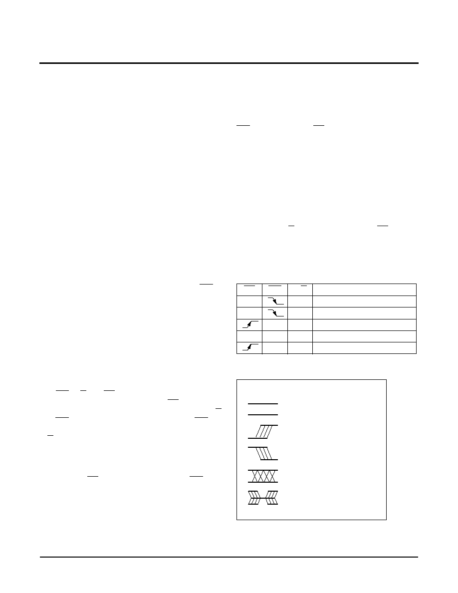
MODE SELECTION
SYMBOL TABLE
CS
INC
U/D
Mode
L
H
Wiper Up
L
L
Wiper Down
H
X
Store Wiper Position
H
X
X
Standby Current
L
X
No Store, Return to Standby
WAVEFORM
INPUTS
OUTPUTS
Must be
steady
Will be
steady
May change
from Low to
High
Will change
from Low to
High
May change
from High to
Low
Will change
from High to
Low
Don't Care:
Changes
Allowed
Changing:
State Not
Known
N/A
Center Line
is High
Impedance
X9C303
Characteristics subject to change without notice.
4 of 10
REV 1.1 4/27/01
www.xicor.com
ABSOLUTE MAXIMUM RATINGS
Temperature under bias ....................≠65∞C to +135∞C
Storage temperature .........................≠65∞C to +150∞C
Voltage on CS, INC, U/D and V
CC
with respect to V
SS
.................................. ≠1V to +7V
Voltage on V
H
and V
L
referenced to V
SS
................................... ≠8V to +8V
V = |V
H
≠V
L
| X9C303 .......................................... 10V
Lead temperature (soldering, 10 seconds)...... +300∞C
Wiper current ..................................................... ±1mA
COMMENT
Stresses above those listed under "Absolute Maximum
Ratings" may cause permanent damage to the device.
This is a stress rating only; functional operation of the
device (at these or any other conditions above those
listed in the operational sections of this specification)
is not implied. Exposure to absolute maximum rating
conditions for extended periods may affect device reli-
ability.
ANALOG CHARACTERISTICS
Electrical Characteristics
End-to-end resistance tolerance ....................... ±15%
Power rating at 25∞C X9C303 ........................... 10mW
Wiper current ............................................ ±1mA Max.
Typical wiper resistance ...........................40
at 1mA
Typical resistor
noise ........................ 23 nV (RMS)/˜Hz at 1kHzPHZ
Typical charge pump noise.. 20 mV (RMS) @ 2.5 MHz
Relative Variation
Relative variation is a measure of the error in step size
between
taps = log (V
w(n)
) ≠ log (V
w(n-1)
) = 0.045 ± 0.003
for tap n = 2 ≠ 99
Temperature Coefficient
(≠40∞C to +85∞C) X9C303 .......... ±400 ppm/∞C Typical
Ratiometric temperature coefficient ..............±20 ppm
Wiper Adjustability
Unlimited Wiper Adjustment (Non-Store operation)
Wiper Position Store
Operations ...................100,000 Data Changes per Bit
Physical Characteristics
Marking Includes
Manufacturer's Trademark
Resistance Value or Code
Date Code
Typical Electrical Taper
100.0%
90.0%
80.0%
70.0%
60.0%
50.0%
40.0%
30.0%
20.0%
10.0%
0.0%
% Total Resistance
0
3
6
9
12
15
18
21
24
27
30
33
36
39
42
45
48
51
54
57
60
63
66
69
72
75
78
81
84
87
90
93
96
99
Tap
R(V
H
≠V
W
)
R(V
W
≠V
L
)

X9C303
Characteristics subject to change without notice.
5 of 10
REV 1.1 4/27/01
www.xicor.com
Test Circuit #1
Test Point
V
W
V
H
V
L
V
S
D.C. OPERATING CHARACTERISTICS
(Over recommended operating conditions unless otherwise specified.)
Standard Parts
Notes:
(1) Typical values are for T
A
= 25∞C and nominal supply voltage.
(2) This parameter is periodically sampled and not 100% tested.
Symbol
Parameter
Limits
Unit
Test Conditions
Min.
Typ.
1
Max.
I
CC
V
CC
active current
1
3
mA
CS = V
IL
, U/D = V
IL
or V
IH
and
INC = 0.4V to 2.4V @ max. t
CYC
I
SB
Standby supply current
200
750
µA
CS = V
CC
≠ 0.3V, U/D and INC
= V
SS
or V
CC
≠ 0.3V
I
LI
CS, INC, U/D input leakage
current
±10
µA
V
IN
= V
SS
to V
CC
V
IH
CS, INC, U/D input HIGH
voltage
2
V
CC
+ 1
V
V
IL
CS, INC, U/D input LOW
voltage
≠1
0.8
V
R
W
Wiper resistance
40
100
Max. Wiper Current ±1mA
V
H
V
H
terminal voltage
≠5
+5
V
V
L
V
L
terminal voltage
≠5
+5
V
C
IN
(2)
CS, INC, U/D input capacitance
10
pF
V
CC
= 5V, V
IN
= V
SS
,
T
A
= 25∞C, f = 1MHz
C
H
/C
L
/C
W
Potentiometer capacitance
10/10/25
pF
See Circuit 3
Part Number
Maximum Resistance
Wiper Increments
Minimum Resistance
X9C303
32K
Log Taper
40
Typical
RECOMMENDED OPERATING CONDITIONS
Temperature
Min.
Max.
Commercial
0∞C
+70∞C
Industrial
≠40∞C
+85∞C
Military
≠55∞C
+125∞C
Supply Voltage
Limits
X9C303
5V ±10%
Test Circuit #2
Force
V
L
V
W
V
H
Test Point
Current
Circuit #3SPICE Macro Model
C
W
R
TOTAL
R
H
R
L
C
H
R
W
10pF
C
L
10pF
25pF
X9C303
Characteristics subject to change without notice.
6 of 10
REV 1.1 4/27/01
www.xicor.com
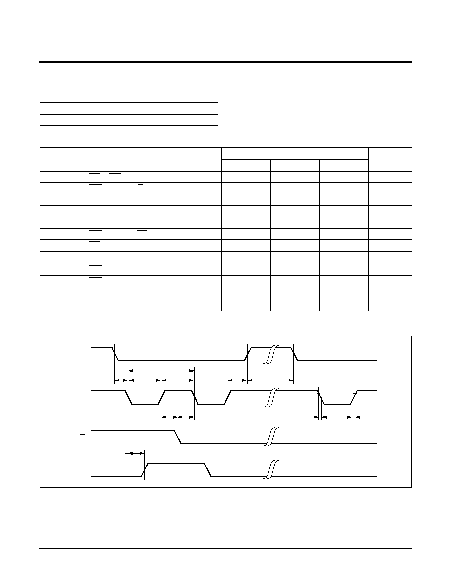
A.C. CONDITIONS OF TEST
A.C. OPERATING CHARACTERISTICS (Over recommended operating conditions unless otherwise specified)
A.C. TIMING
Notes: (3) Typical values are for T
A
= 25∞C and nominal supply voltage.
(4) This parameter is periodically sampled and not 100% tested.
(5) MI in the A.C. timing diagram refers to the minimum incremental change in the V
W
output due to a change in the wiper position.
Input pulse levels
0V to 3V
Input rise and fall times
10ns
Input reference levels
1.5V
Symbol
Parameter
Limits
Unit
Min.
Typ.
3
Max.
t
Cl
CS to INC setup
100
ns
t
lD
INC HIGH to U/D change
100
ns
t
DI
U/D to INC setup
2.9
µs
t
lL
INC LOW period
1
µs
t
lH
INC HIGH period
1
µs
t
lC
INC inactive to CS inactive
1
µs
t
CPH
CS deselect time
20
ms
t
IW
INC to V
W
change
100
500
µs
t
CYC
INC cycle time
4
µs
t
R,
t
F
4
INC input rise and fall time
500
ns
t
PU
4
Power up to wiper stable
500
µs
t
R
V
CC
4
V
CC
power-up rate
0.2
50
mV/µs
CS
INC
U/D
V
W
t
CI
t
IL
t
IH
t
CYC
t
ID
t
DI
t
IW
MI
(8)
t
IC
t
CPH
t
F
t
R
10%
90%
90%
X9C303
Characteristics subject to change without notice.
7 of 10
REV 1.1 4/27/01
www.xicor.com
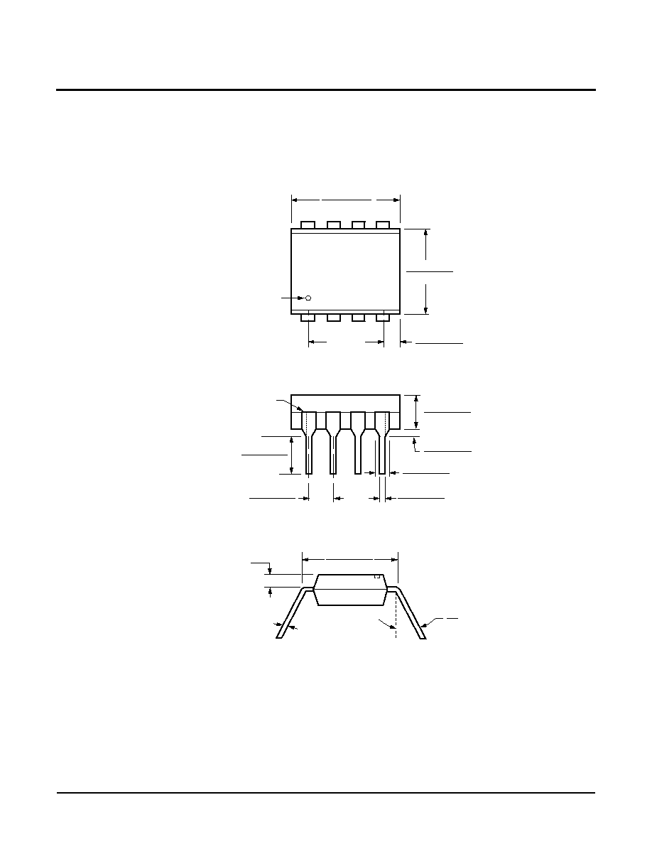
PACKAGING INFORMATION
NOTE:
1. ALL DIMENSIONS IN INCHES (IN PARENTHESES IN MILLIMETERS)
2. PACKAGE DIMENSIONS EXCLUDE MOLDING FLASH
0.020 (0.51)
0.016 (0.41)
0.150 (3.81)
0.125 (3.18)
0.110 (2.79)
0.090 (2.29)
0.430 (10.92)
0.360 (9.14)
0.300
(7.62) Ref.
Pin 1 Index
0.145 (3.68)
0.128 (3.25)
0.025 (0.64)
0.015 (0.38)
Pin 1
Seating
0.065 (1.65)
0.045 (1.14)
0.260 (6.60)
0.240 (6.10)
0.060 (1.52)
0.020 (0.51)
Typ. 0.010 (0.25)
0∞
15∞
8-Lead Plastic Dual In-Line Package Type P
Half Shoulder Width On
All End Pins Optional
.073 (1.84)
Max.
0.325 (8.25)
0.300 (7.62)
Plane
X9C303
Characteristics subject to change without notice.
8 of 10
REV 1.1 4/27/01
www.xicor.com
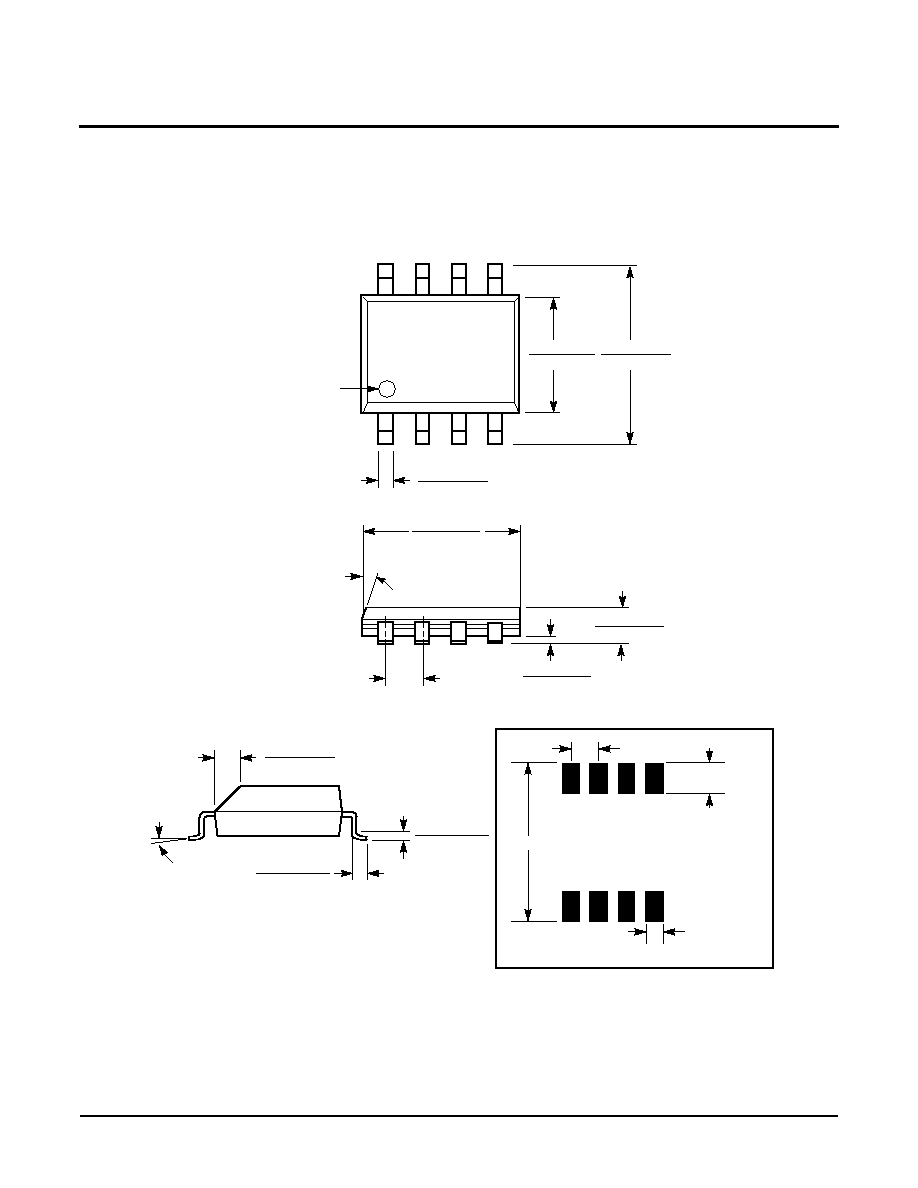
PACKAGING INFORMATION
0.150 (3.80)
0.158 (4.00)
0.228 (5.80)
0.244 (6.20)
0.014 (0.35)
0.019 (0.49)
Pin 1
Pin 1 Index
0.010 (0.25)
0.020 (0.50)
0.050 (1.27)
0.188 (4.78)
0.197 (5.00)
0.004 (0.19)
0.010 (0.25)
0.053 (1.35)
0.069 (1.75)
(4X) 7∞
0.016 (0.410)
0.037 (0.937)
0.0075 (0.19)
0.010 (0.25)
0∞ - 8∞
X 45∞
8-Lead Plastic Small Outline Gull Wing Package Type S
NOTE: ALL DIMENSIONS IN INCHES (IN PARENTHESES IN MILLIMETERS)
0.250"
0.050" Typical
0.050"
Typical
0.030"
Typical
8 Places
FOOTPRINT
X9C303
Characteristics subject to change without notice.
9 of 10
REV 1.1 4/27/01
www.xicor.com
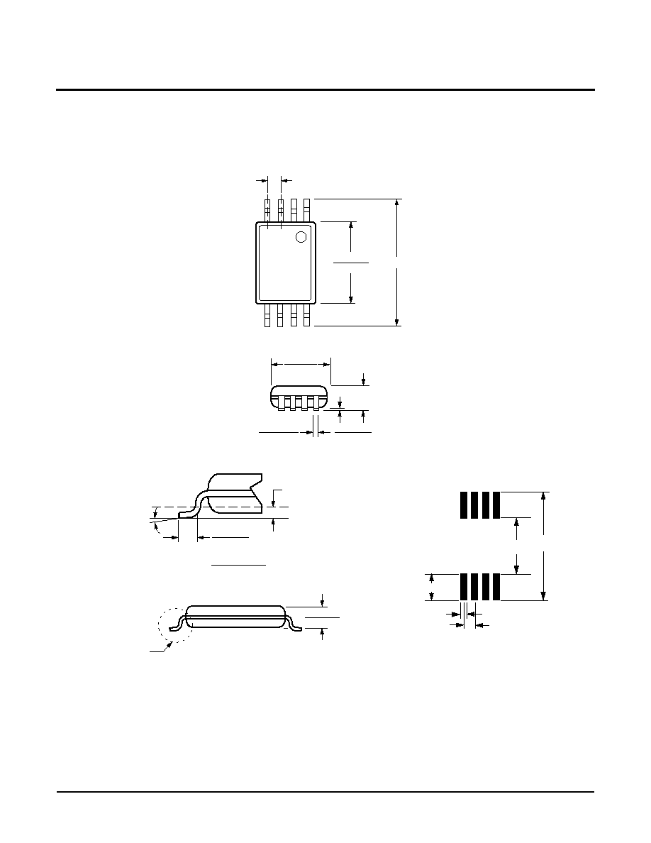
PACKAGING INFORMATION
NOTE: ALL DIMENSIONS IN INCHES (IN PARENTHESES IN MILLIMETERS)
8-Lead Plastic, TSSOP, Package Type V
See Detail "A"
.031 (.80)
.041 (1.05)
.169 (4.3)
.177 (4.5)
.252 (6.4) BSC
.025 (.65) BSC
.114 (2.9)
.122 (3.1)
.002 (.05)
.006 (.15)
.047 (1.20)
.0075 (.19)
.0118 (.30)
0∞ ≠ 8∞
.010 (.25)
.019 (.50)
.029 (.75)
Gage Plane
Seating Plane
Detail A (20X)
(4.16) (7.72)
(1.78)
(0.42)
(0.65)
All Measurements Are Typical

X9C303
Characteristics subject to change without notice.
10 of 10
REV 1.1 4/27/01
www.xicor.com
©Xicor, Inc. 2001 Patents Pending
LIMITED WARRANTY
Devices sold by Xicor, Inc. are covered by the warranty and patent indemnification provisions appearing in its Terms of Sale only. Xicor, Inc. makes no warranty,
express, statutory, implied, or by description regarding the information set forth herein or regarding the freedom of the described devices from patent infringement.
Xicor, Inc. makes no warranty of merchantability or fitness for any purpose. Xicor, Inc. reserves the right to discontinue production and change specifications and prices
at any time and without notice.
Xicor, Inc. assumes no responsibility for the use of any circuitry other than circuitry embodied in a Xicor, Inc. product. No other circuits, patents, or licenses are implied.
COPYRIGHTS AND TRADEMARKS
Xicor, Inc., the Xicor logo, E
2
POT, XDCP, XBGA, AUTOSTORE, Direct Write cell, Concurrent Read-Write, PASS, MPS, PushPOT, Block Lock, IdentiPROM,
E
2
KEY, X24C16, SecureFlash, and SerialFlash are all trademarks or registered trademarks of Xicor, Inc. All other brand and product names mentioned herein are
used for identification purposes only, and are trademarks or registered trademarks of their respective holders.
U.S. PATENTS
Xicor products are covered by one or more of the following U.S. Patents: 4,326,134; 4,393,481; 4,404,475; 4,450,402; 4,486,769; 4,488,060; 4,520,461; 4,533,846;
4,599,706; 4,617,652; 4,668,932; 4,752,912; 4,829,482; 4,874,967; 4,883,976; 4,980,859; 5,012,132; 5,003,197; 5,023,694; 5,084,667; 5,153,880; 5,153,691;
5,161,137; 5,219,774; 5,270,927; 5,324,676; 5,434,396; 5,544,103; 5,587,573; 5,835,409; 5,977,585. Foreign patents and additional patents pending.
LIFE RELATED POLICY
In situations where semiconductor component failure may endanger life, system designers using this product should design the system with appropriate error detection
and correction, redundancy and back-up features to prevent such an occurrence.
Xicor's products are not authorized for use in critical components in life support devices or systems.
1. Life support devices or systems are devices or systems which, (a) are intended for surgical implant into the body, or (b) support or sustain life, and whose failure to
perform, when properly used in accordance with instructions for use provided in the labeling, can be reasonably expected to result in a significant injury to the user.
2. A critical component is any component of a life support device or system whose failure to perform can be reasonably expected to cause the failure of the life
support device or system, or to affect its safety or effectiveness.
Ordering Information
Temperature Range
Blank = Commercial = 0∞C to +70∞C
I = Industrial = ≠40∞C to +85∞C
Package
P = 8-Lead Plastic DIP
S8 = 8-Lead SOIC
V8 = 8-Lead TSSOP
X9C303
X
X