 | –≠–ª–µ–∫—Ç—Ä–æ–Ω–Ω—ã–π –∫–æ–º–ø–æ–Ω–µ–Ω—Ç: XK3100 | –°–∫–∞—á–∞—Ç—å:  PDF PDF  ZIP ZIP |
©
Xicor, Inc. 1994 ≠ 1999 Patents Pending
9900-3016.1 11/8/99 CM
1
Characteristics subject to change without notice
XK3100
3 or 4 Cell Li-Ion Battery System Development Kit
DESCRIPTION
The XK3100 is a development board that features the
Xicor X3100 Lithium Ion battery protection and monitor
IC. For use in battery packs consisting of 3 or 4 Lithium-
Ion battery cells, the X3100 provides:
∑ internal over-voltage, under-voltage, and over-current
protection circuitry
∑ internal EEPROM memory
∑ circuits for externally monitoring cell voltages and pack
current, including a current sense amplifier for higher
resolution current measurements,
∑ an internal voltage regulator, and
∑ internal drive circuitry for switching external FET
devices used to control cell charge, discharge, and cell
voltage balancing.
The XK3100 board provides the external devices
needed to control the battery pack and adds a
microcontroller. This microcontroller talks to the PC
through a 2-wire interface. The microcontroller provides
a mechanism for interrogating the X3100 status,
monitoring the pack voltages and current and controlling
protection settings. The board provides an interface for
attaching microcontroller development tools. This will
facilitate the development of more complete battery pack
software. Future revisions of the software and
microcontroller firmware, may include: full SMBus
support, battery gas gauging, cell balancing, and history
tracking.
The XK3100 user interface consists of a Graphical User
Interface program running on Windows 95/98. This
software provides a menu driven method of setting the
programmable elements of the X3100, monitoring the
status of the batteries and reading the on-chip
EEPROM. The XK3100 board and software will monitor
and control all features of the X3100 device.
FEATURE
BENEFIT
∑ Self contained Development Board
(batteries not included)
∑ Speed system development
∑ X3100 and microcontroller control
∑ Maximum flexibility to explore alternative
implementations.
∑ Evaluate algorithmic trade-offs for Gas Gauging
and Cell Balancing functions
∑ External components provided
∑ Minimize battery pack development issues
∑ PC connection and software
∑ Simple interface to special X3100 functions
∑ SMBus hardware connection
∑ Speeds development of industry standard Smart
Battery interface
Included in the XK3100
∑ Fully assembled and tested board, complete with
microcontroller, FETs, sense resistor and regulator cir-
cuits.
∑ Win95/98 compatible executable program providing
the user interface to the hardware.
∑ Cable from the PC parallel port to the XK3100
∑ Two samples of the X3100
∑ Users Manual
∑ X3100 Data Sheet
∑ Board schematics and layout information
∑ Two application notes.

XK3100
2
©
Xicor, Inc. 1994 ≠ 1999 Patents Pending
PRELIMINARY REVISION 5.0
Characteristics subject to change without notice
SYSTEM BLOCK DIAGRAM
BOARD DESCRIPTION:
Safety/Battery Monitor:
∑ X3100V8 (One on-board, one additional sample)
With the following features:
∑
Selectable over-voltage, under-voltage, and over-
current protection circuitry
∑
4K bits EEPROM memory
∑
Analog MUX, with output, to externally monitor cell
voltages and pack current
∑
Current sense amplifier with x10, x25, x80, x160
selectable gain.
∑
5V +/- 0.5% voltage regulator,
∑
Automatic and manual control of charge/discharge
FETs
∑
Manual control of cell voltage balancing FETs.
Microcontroller:
∑ Mitsubishi M37516M4
With the following features:
∑
Memory
-
ROM: 16 Kilobytes. Preprogrammed with board
firmware.
-
RAM: 512 bytes
∑
A-D Converter:
-
Successive Approximation architecture.
-
10-bit resolution, +/- 1 LSB.
-
Eight analog channels available.
-
12.5µs typical conversion time for ADC.
∑
Timers:
-
Four 8-bit and one 16-bit watchdog timer availa-
ble.
-
All are multi-purpose: designer can choose from
timer, event count, pulse output, or pulse period
measurement mode.
∑
Serial I/O:
-
SPI port.
-
I
2
C port:
∑
Low-power Dissipation:
-
Multiple speed modes possible to conserve bat-
tery power.
-
Less than 1uA in lowest power mode
∑
Development tools readily available.
Emulator Support:
The XK3100 board provides a socket that accepts the
Mitsubishi development tools and a single switch that
selects the on-board microcontroller or the emulation
system. This facilitates the development of custom
routines, such as SMBus support, cell balancing or fuel
gauging.
Interface between PC and development board
∑ Parallel interface from PC to XK3100 board. Converts
to I
2
C on board to connect to the microcontroller.
XK3100 Development Board
PC
Parallel
Port
Micr
ocontr
oller
SPI
I/F
SMBus
I/F
Buffers
uC Emulator
Socket
Development
Area
Cells
3
4
uC
EMU
B-
P-
B+
P+
P+
P-
X3100
XK3100
3
©
Xicor, Inc. 1994 ≠ 1999 Patents Pending
PRELIMINARY REVISION 5.0
Characteristics subject to change without notice
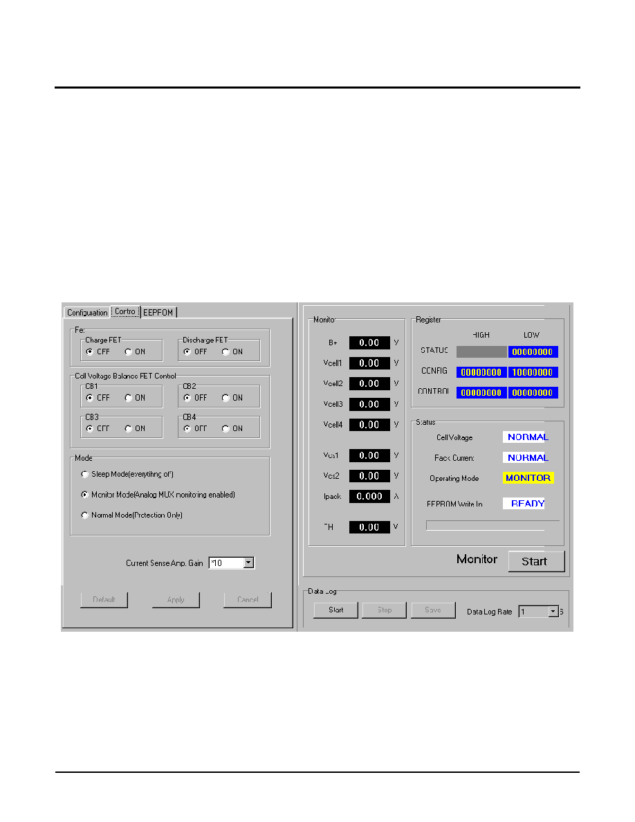
SOFTWARE DESCRIPTION
∑ Windows 95/98 based software provides:
∑
Menu driven interface.
∑
Full time display that shows battery information on a
periodic basis. Information shown includes voltage
on each cell, Rsense voltage (both directions),
computed current, Computed B+ voltage, tempera-
ture, control and configuration bits and pack status.
There are 6 sampling rates from 1 second to 120
seconds and samples may be recorded in a file.
This provides the ability to automatically monitor a
test setup of battery performance over a long period
of time.
∑
Tabular selection of screens for setting the program-
mable characteristics of the X3100. This includes
setting over-voltage, under-voltage and over-current
thresholds, selecting sleep and power down modes,
direct control of the charge/discharge FETs, direct
control of the cell balancing FETs, and specifying
the gain of the cell current amplifier.
∑
A tabular screen selection also allows the reading
and writing of the EEPROM array.
Graphical User Interface
The following diagram shows a sample screen from the
XK3100 development kit.
XK3100
4
©
Xicor, Inc. 1994 ≠ 1999 Patents Pending
PRELIMINARY REVISION 5.0
Characteristics subject to change without notice
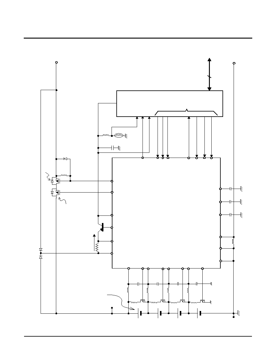
BOARD DIAGRAM
100
.
Vss
VCS1
VCS2
O
V
T
UVT
OCT
VCELL1
CB1
CB3
VCELL4
VCELL3
X3100
CB2
Vcc
RGP
RGC
RGO
O
VP/LMON
UVP/
AS0
AS1
AS2
AO
S0
SCL
CS
SI
GP
I/O
M37516
100
100
100
100
100
100
100
Q1
Q2
Q3
Q4
0.01uF
0.01uF
0.01uF
0.01uF
50
50mA max
KT
A1661
Si4435D
Y
Si4435D
Y
1M
D
1
P+
P-
HOST
I/F
D
3
D
2
A/D Ref
erence
A/D Input
A/D Input
10K
R
T
V
T
VCELL2
R
SENSE
3 or 4
Li-Ion cells
Discharge FET
Charge FET
Vcc
V
RGO
Input
D
ATA
CB4
In the case that
3 cells are used
VCELL4
MUST be tied to
Vss
.
B+
B-
OCP
50m
0.1uF
0.1uF
0.1uF
Q1-Q4 = 2N7002
2
Q5
Q7