Document Outline
- Table of Contents
- Product Selection
- Data Sheet Alpha
- Ap Note Alpha
XM20C64
1
©Xicor, Inc. 1991, 1995, 1996 Patents Pending
Characteristics subject to change without notice
3874-1.6 6/20/96 T0/C2/D0 NS
High Speed AUTOSTORE
TM
NOVRAM
64K
XM20C64
8K x 8
FEATURES
∑
High Speed: t
AA
= 55ns
∑
NO Batteries!!
∑
Low Power CMOS
∑
AUTOSTORE
TM
NOVRAM
--Automatically Stores RAM data to E
2
PROM
upon Power-fail Detection
∑
Open Drain AUTOSTORE Output Pin
--Provides Interrupt or Status Information
--Linkable to System Reset Circuitry
∑
Auto Recall
--Automatically Recalls E
2
PROM Data During
Power-on
∑
Fully Decoded Module
∑
Full Military Temperature Range
-- ≠55
∞
C to +125
∞
C
∑
High Reliability
--Endurance: 1,000,000 Nonvolatile Store Cycles
--Data Retention: 100 Years
∑
ESD Protection
--
2KV All Pins
∑
Also Available in 66 Pin PUMA Package
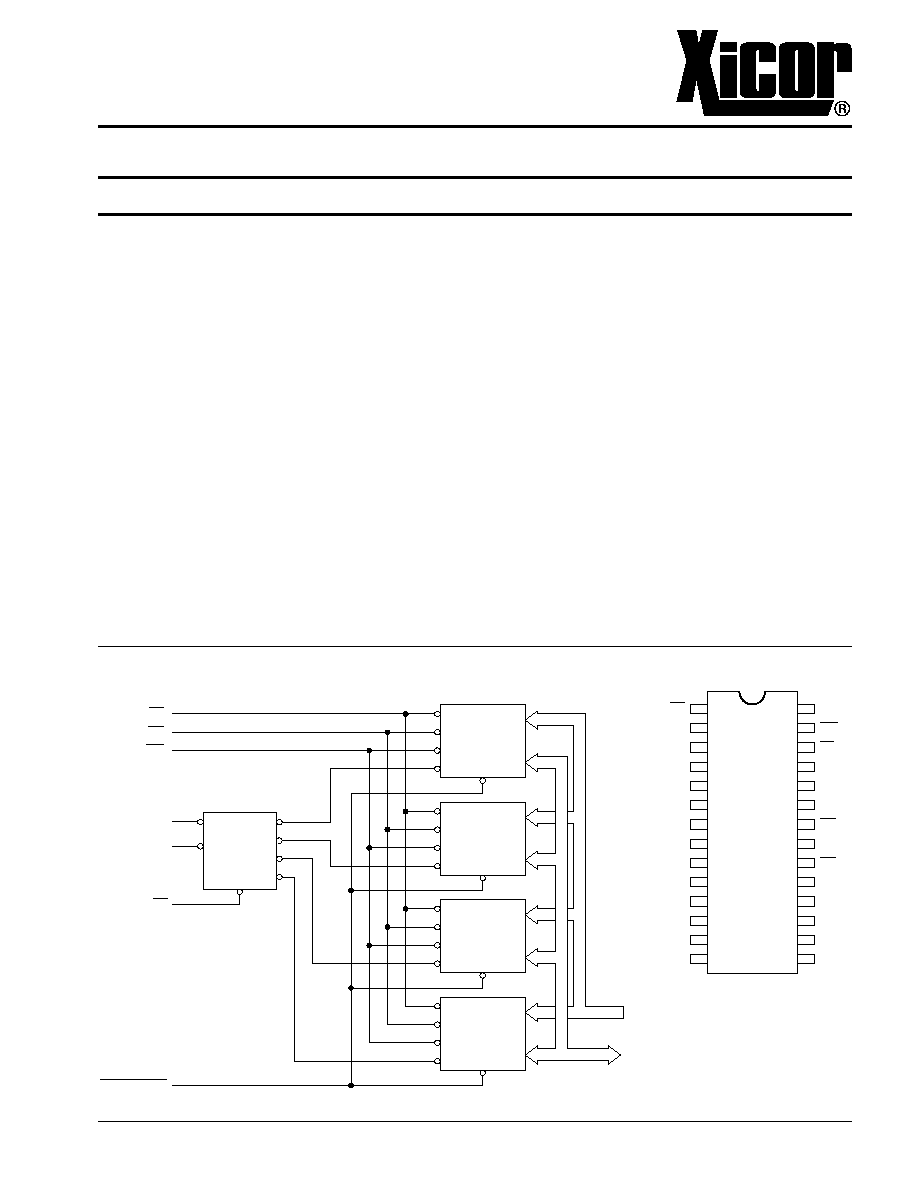
DESCRIPTION
The XM20C64 is a high speed nonvolatile RAM Module.
It is comprised of four Xicor X20C16 high speed
NOVRAMs, a high speed decoder and decoupling
capacitors mounted on a co-fired multilayered Ceramic
substrate. The XM20C64 is configured 8K x 8 and is fully
decoded. The module is a 28-lead DIP conforming to the
industry standard pinout for SRAMs.
The XM20C64 fully supports the AUTOSTORE feature,
providing hands-off automatic storing of RAM data
into E
2
PROM when V
CC
falls below the AUTOSTORE
threshold.
The XM20C64 is a highly reliable memory component,
supporting unlimited writes to RAM, a minimum 1,000,000
store cycles and a minimum 100 year data retention.
3874 FHD F01
NE
OE
WE
CE
A0≠A10
I/O
NE
OE
WE
CE
A0≠A10
I/O
NE
OE
WE
CE
A0≠A10
I/O
NE
OE
WE
CE
A0≠A10
I/O
Y0
Y1
Y2
Y3
1
A1
A0
2
3
A12
A11
CE
7
AUTOSTORE
WE
OE
NE
A0≠A10
I/O0≠I/O7
6
5
4
23
31
25
2
30
23
31
25
2
30
23
31
25
2
30
23
31
25
2
30
AUTOSTORETM NOVRAM is a trademark of Xicor, Inc.
FUNCTIONAL DIAGRAM
PIN CONFIGURATION
3874 FHD F02.1
NE
A12
A7
A6
A5
A4
A3
A2
A1
A0
I/O0
I/O1
I/O2
VSS
1
2
3
4
5
6
7
8
9
10
11
12
13
14
28
27
26
25
24
23
22
21
20
19
18
17
16
15
VCC
WE
AS
A8
A9
A11
OE
A10
CE
I/O7
I/O6
I/O5
I/04
I/O3

XM20C64
2
PIN DESCRIPTIONS
Addresses (A
0
-A
12
)
The address inputs select an 8-bit memory location
during read and write operations.
Chip Enable (
CE
)
The chip enable input must be LOW to enable all read,
write and user requested nonvolatile operations.
Output Enable (
OE
)
During normal RAM operations
OE
controls the data
output buffers. If a hardware nonvolatile operation is
selected (
NE
=
CE
= LOW) and
OE
strobes LOW, a
recall operation will be initiated.
OE
LOW will always disable a STORE operation regard-
less of the state of
NE
,
WE
, and
CE
so long as the
internal transfer has not commenced.
Write Enable (
WE
)
During normal RAM operations
WE
=
CE
= LOW will
cause data to be written to the RAM address pointed to
by the A
0
-A
12
inputs.
Nonvolatile Enable (
NE
)
The nonvolatile input controls the transfer of data from
the E
2
PROM array to the RAM array, when strobed
LOW in conjunction with
CE
=
OE
= LOW.
Data In/Data Out (I/O
0
-I/O
7
)
Data is written to or read from the X20C64 through the
I/O pins. The I/O pins are placed in the high impedance
state when either
CE
or
OE
is HIGH or when
NE
is LOW.
AUTOSTORE Output (
AS
)
AS
is an open-drain output. When it is asserted (driving
LOW) it indicates V
CC
has fallen below the AUTOSTORE
threshold and an internal store operation has been
initiated. Because
AS
is an open drain output it may be
wire-ORed with multiple open drain outputs and used as
an interrupt input to a microprocessor.
DEVICE OPERATION
NOVRAM operations are identical to those of a standard
SRAM. When
OE
and
CE
are asserted data is presented
at the I/Os from the address location pointed to by the
A
0
≠A
12
inputs.
RAM write operations are initiated and the address input
is latched by the HIGH to LOW transition of
CE
or
WE
,
whichever occurs last. Data is latched on the rising edge
of either
CE
or
WE
, whichever occurs first.
An array recall, E
2
PROM data transferred to RAM, is
initiated whenever
OE
=
NE
=
CE
= LOW. A recall is also
performed automatically upon power-up.
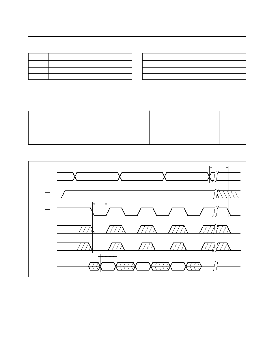
Command Sequence Operations
The X20C64 employs a version of the industry standard
Software Data Protection (SDP). The end user can
select various options for transferring data from RAM
into the E
2
PROM array.
All command sequences are comprised of three specific
data/address write operations performed with
NE
LOW.
A Store operation can be directly selected by issuing a
Store command. The user may also enable and disable
the AUTOSTORE function through the software data
protection sequence. Refer to Table 1 below for a
complete description of the command sequence.
Operational Notes
The X20C64 should be viewed as a subsystem when
writing software for the various store operations. The
module contains four discrete components each need-
ing to be set to the required state individually. The two
high order address bits (A
11
and A
12
) select only one of
the four components.
XM20C64
3
TABLE 1
Step
Operation
A
0
≠A
10
*
Data Pattern
1
Write
555
AA
2
Write
2AA
55
3
Write
555
Command
3874 PGM T11
TABLE 2
Command
Function
CC[H]
Enable Autostore
CD[H]
Disable Autostore
33[H]
Store Operation
3874 PGM T12.2
* It should be noted, the high order addresses should remain
stable during the operations. It should also be noted that these
commands are not global, that is only one device on the module
will be affected by each command operation.
Command Sequence
Note:
All Write Command Sequence timings must conform to the standard write timing requirements.
Command Sequence Timing Limits
Limits
Symbol
Parameter
Min.
Max.
Units
t
STO
Store Time
5
ms
t
SP
Command Write Pulse Width
50
ns
t
SPH
Inter Command Delay
55
ns
3874 PGM T01.1
3874 FHD F03.1
ADDRESS
555
2AAA
555
OE
CE
WE
NE
DATA IN
tSTO
tSP
CMD
55
AA
tDH
tDS
XM20C64
4
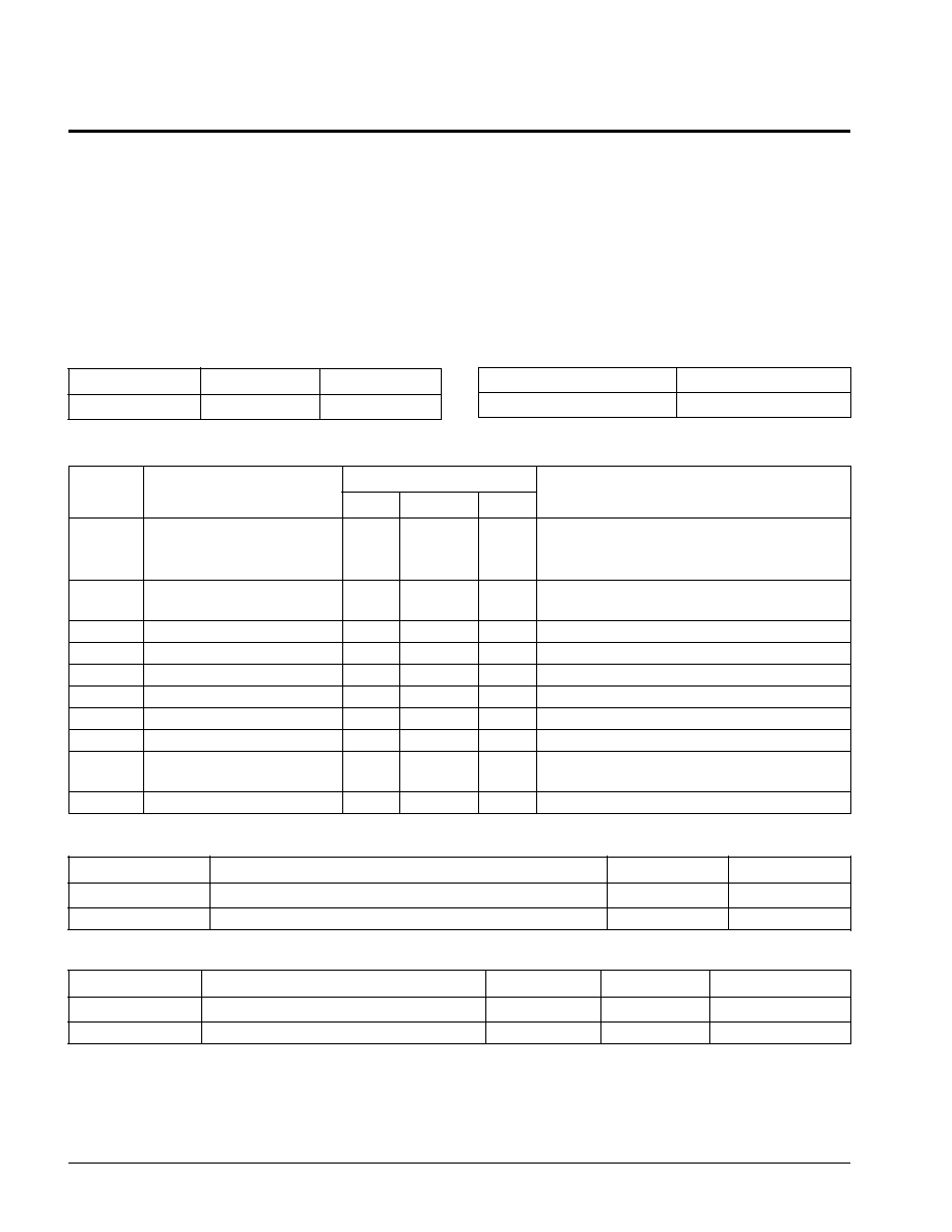
D.C. OPERATING CHARACTERISTICS (Over recommended operating conditions unless otherwise specified.)
Limits
Symbol
Parameter
Min.
Max.
Units
Test Conditions
l
CC1
V
CC
Active Current
100
mA
NE
=
WE
+ V
IH
,
CE
=
OE
= V
IL,
Address Inputs = TTL Inputs @ f = 20MHz
All I/Os = Open
I
CC2
V
CC
Active Current
10
mA
All Inputs = V
IH,
All I/Os = Open
(AUTOSTORE)
I
SB
V
CC
Standby Current
1.5
mA
All Inputs = V
CC
≠0.3V All I/Os = Open
I
LI
Input Leakage Current
10
µ
A
V
IN
= V
SS
to V
CC
I
LO
Output Leakage Current
10
µ
A
V
IN
= V
SS
to V
CC
,
CE
= V
IH
V
IL
(1)
Input LOW Voltage
≠0.5
0.8
V
V
IH
(1)
Input HIGH Voltage
2
V
CC
+ 0.5
V
V
OL
Output LOW Voltage
0.4
V
I
OL
= 5mA
V
OLAS
AUTOSTORE Output
0.4
V
I
OLAS
= 1mA
Voltage
V
OH
Output HIGH Voltage
2.4
V
I
OH
= ≠4mA
3874 PGM T08.2
ABSOLUTE MAXIMUM RATINGS*
Temperature Under Bias .................. ≠65
∞
C to +125
∞
C
Storage Temperature ....................... ≠65
∞
C to +125
∞
C
Voltage on any Pin with
Respect to V
SS ............................................
≠1V to +7V
Lead Temperature
(Soldering, 10 seconds) .............................. 300
∞
C
*COMMENT
Stresses above those listed under "Absolute Maximum
Ratings" may cause permanent damage to the module.
This is a stress rating only and the functional operation of
the module at these or any other conditions above those
indicated in the operational sections of this specification is
not implied. Exposure to absolute maximum rating condi-
tions for extended periods may affect module reliability.
Supply Voltage
Limits
XM20C64
5V
±
10%
3874 PGM T07
RECOMMENDED OPERATING CONDITIONS
Temperature
Min.
Max.
Military
≠55
∞
C
+125
∞
C
3874 PGM T06
CAPACITANCE T
A
= +25
∞
C, f = 1MHz, V
CC
= 5V.
Symbol
Test
Max.
Units
Conditions
C
I/O
(2)
Input/Output Capacitance
40
pF
V
I/O
= 0V
C
IN
(2)
Input Capacitance
24
pF
V
IN
= 0V
3874 PGM T10.1
POWER-UP TIMING
Symbol
Parameter
Max.
Units
t
PUR
Power-Up (V
CC
Min.) to RAM Operation
500
µ
s
t
PUST
Power-Up (V
CC
Min.) to Store Operation
5
ms
3874 PGM T09
Notes: (1) V
IL
min. and V
IH
max. are for reference only and are not tested.
(2) This parameter is periodically sampled and not 100% tested.
XM20C64
5
A.C. CHARACTERISTICS (Over the recommended operating conditions unless otherwise specified)
Read Cycle Limits
Limits
Symbol
Parameter
Min.
Max.
Units
t
RC
Read Cycle Time
55
ns
t
CE
Chip Enable Access Time
55
ns
t
AA
Address Access Time
55
ns
t
OE
Output Enable Access Time
30
ns
t
LZ
(3)
CE
Low to Output in Low Z
0
ns
t
OLZ
(3)
OE
Low to Output in Low Z
0
ns
t
HZ
(3)
CE
High to Output in Low Z
0
25
ns
t
OHZ
(3)
OE
High to Output in Low Z
0
25
ns
t
OH
Output Hold
0
ns
3874 PGM T03
MODE SELECTION
CE
WE
NE
OE
Mode
I/O State
Power
H
X
X
X
Module Not Selected
High Z
Standby
L
H
H
L
Read RAM Active
Data Output
Active
L
L
H
X
Write RAM
Data Input
Active
L
L
L
H
Issue Software Command
Data Input
Active
L
H
H
H
Output Disabled
High Z
Active
L
H
L
L
Hardware Array Recall
High Z
Active
L
H
L
H
No Operation
High Z
Active
L
L
L
L
Not Allowed
High Z
Active
3874 PGM T04.1
Read Cycle Timing Diagram
3874 FHD F05
Note:
(3) t
LZ
min., t
HZ
min., t
OLZ
min., and t
OHZ
min. are periodically sampled and not 100% tested. t
HZ
max. and t
OHZ
max. are
measured from the point when
CE
or
OE
return high (whichever occurs first) to the time when the outputs are no longer driven.
tCE
tRC
ADDRESS
CE
OE
tOE
tLZ
tOLZ
tOH
tAA
tHZ
tOHZ
I/O
tOE
XM20C64
6
tWC
tCW
tAS
tWP
tDS
tDH
tOW
tWR
DATA VALID
ADDRESS
OE
CE
WE
DATA OUT
DATA IN
Write Cycle Limits
Limits
Symbol
Parameter
Min.
Max.
Units
t
WC
Write Cycle time
55
ns
t
WP
WE
Pulse Width
40
ns
t
CW
CE
Pulse Width
40
ns
t
AS
Address Setup
0
ns
t
DS
Data Setup
25
ns
t
DH
Data Hold
0
ns
t
OW
Output Active from End of Write
5
ns
t
WR
End of Write to Read
0
ns
3874 PGM T02
Write Cycle Timing Diagram
3874 FHD F04

XM20C64
7
Array Recall Timing
Limits
Symbol
Parameter
Min.
Max.
Units
t
RCC
Array Recall Time
10
µ
s
t
RCP
Recall Strobe Pulse Width
50
ns
t
RWE
Delay From
WE
HIGH to Recall
0
ns
3874 PGM T05.1
Note:
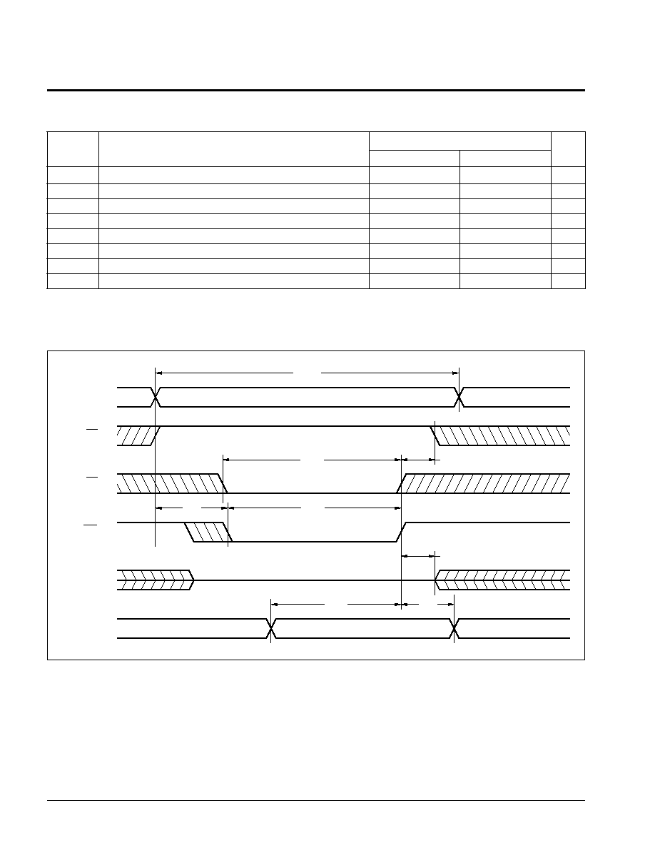
The recall sequence must be repeated for each memory component individually. This is accomplished by sequencing through the
Array Recall Cycle with all four combinations of A
11
, and A
12
.
Array Recall Cycle
3874 FHD F06.1
EQUIVALENT TEST LOAD CIRCUIT
SYMBOL TABLE
WAVEFORM
INPUTS
OUTPUTS
Must be
steady
Will be
steady
May change
from LOW
to HIGH
Will change
from LOW
to HIGH
May change
from HIGH
to LOW
Will change
from HIGH
to LOW
Don't Care:
Changes
Allowed
Changing:
State Not
Known
N/A
Center Line
is High
Impedance
ADDRESS
NE
OE
WE
CE
DATA I/O
tRCC
tRCP
tRWE
3874 FHD F07.2
735
318
OUTPUT
30pF
5V
XM20C64
8
PIN CONFIGURATION
3874 ILL F10
I/O8
WE2 I/O15
I/O9
CE2 I/O14
I/O10 GND I/O13
AS
I/O11 I/O12
NE
A10
OE
NC
NC
NC
NC
NC
WE1
NC
VCC
I/O7
I/O0
CE1
I/O6
I/O1
NC
I/O5
I/O2
I/O3
I/O4
I/O24 VCC I/O31
1
12
23
34
45
56
11
22
33
44
55
66
I/O25 CE4 I/O30
I/O26 WE4 I/O29
A6
I/O27 I/O28
A7
A3
A0
A15
A4
A1
A8
A5
A2
A9
WE3 I/O23
I/O16 CE3 I/O22
I/O17 GND I/O21
I/O18 I/O19 I/O20
XM20C64P
PACKAGING INFORMATION
.100 TYP
.100 TYP
.600 TYP
.149+/-.015
.320 MAX
.050
.164
.130
.410
1.09+/-.010 SQ
.040
.050 TYP
.180
3874 ILL F11
ALL MEASUREMENTS IN INCHES
PIN #1
IDENTIFIER
(NOT CHAMFERED)
0.15
.018
XM20C64
9
1.600 MAX.
(40.64)
PIN 1
1.300
±
.005
(33.02
±
0.13)
TOL. NON. ACCUM.
.018
±
.002
(.46
±
.05)
.100
±
.005
(2.54
±
.13)
TYP.
.010
(.25)
MIN.
.295
(6.00)
MAX.
.140
(3.56)
MIN.
+ .002
≠ .001
+ .05
≠ .03
.010
(.25 )
.600
±
.010
(15.24
±
.25)
3926 FHD F40
28-PIN DUAL-IN-LINE PACKAGE CERAMIC LEADLESS CHIP CARRIERS
ON CERAMIC SIDEBRAZED CERAMIC SUBSTRATE
NOTES:
1. ALL DIMENSIONS IN INCHES (IN PARENTHESES IN MILLIMETERS)
2. DIMENSIONS WITH NO TOLERANCE FOR REFERENCE ONLY
.600 (15.24)
.580 (14.73)
PACKAGING INFORMATION

XM20C64
10
NOTES
XM20C64P
XM20C64
11
ORDERING INFORMATION
XM20C64: 2K X 8 CMOS NOVRAM Memory Module
XM20C64
X
X
-X
Device
Access Time
≠55 = 55ns
Temperature Range
Blank = Commercial = 0
∞
C to +70
∞
C
I = Industrial = ≠40
∞
C to +85
∞
C
M = Military = ≠55
∞
C to +125
∞
C
MHR = Military High Rel
Blank = 28 Lead Ceramic DIP Module
P = 66 Pin PUMA Module
LIMITED WARRANTY
Devices sold by Xicor, Inc. are covered by the warranty and patent indemnification provisions appearing in its Terms of Sale only. Xicor, Inc. makes no warranty,
express, statutory, implied, or by description regarding the information set forth herein or regarding the freedom of the described devices from patent infringement.
Xicor, Inc. makes no warranty of merchantability or fitness for any purpose. Xicor, Inc. reserves the right to discontinue production and change specifications and
prices at any time and without notice.
Xicor, Inc. assumes no responsibility for the use of any circuitry other than circuitry embodied in a Xicor, Inc. product. No other circuits, patents, licenses are
implied.
U.S. PATENTS
Xicor products are covered by one or more of the following U.S. Patents: 4,263,664; 4,274,012; 4,300,212; 4,314,265; 4,326,134; 4,393,481; 4,404,475;
4,450,402; 4,486,769; 4,488,060; 4,520,461; 4,533,846; 4,599,706; 4,617,652; 4,668,932; 4,752,912; 4,829, 482; 4,874, 967; 4,883, 976. Foreign patents and
additional patents pending.
LIFE RELATED POLICY
In situations where semiconductor component failure may endanger life, system designers using this product should design the system with appropriate error
detection and correction, redundancy and back-up features to prevent such an occurrence.
Xicor's products are not authorized for use in critical components in life support devices or systems.
1. Life support devices or systems are devices or systems which, (a) are intended for surgical implant into the body, or (b) support or sustain life, and whose
failure to perform, when properly used in accordance with instructions for use provided in the labeling, can be reasonably expected to result in a significant
injury to the user.
2. A critical component is any component of a life support device or system whose failure to perform can be reasonably expected to cause the failure of the life
support device or system, or to affect its safety or effectiveness.