 | –≠–ª–µ–∫—Ç—Ä–æ–Ω–Ω—ã–π –∫–æ–º–ø–æ–Ω–µ–Ω—Ç: XM28C040 | –°–∫–∞—á–∞—Ç—å:  PDF PDF  ZIP ZIP |
Document Outline
- Table of Contents
- Product Selection
- Data Sheet Alpha
- Ap Note Alpha
XM28C040
1
5 Volt, Byte Alterable E
2
PROM
© Xicor, Inc. 1991-1997 Patents Pending
Characteristics subject to change without notice
3873-1.7 6/13/97 T1/C0/D0 SH
TYPICAL FEATURES
∑
High Density 4 Megabit (512K x 8) Module
∑
Access Time of 200ns at ≠55
∞
C to +125
∞
C
∑
Base Memory Component: Xicor X28C010
∑
Pinout Conforms to JEDEC Standard for
4 Megabit E
2
PROM
∑
Fast Write Cycle Times
--256 Byte Page Write
∑
Early End of Write Detection
--
DATA
Polling
--Toggle Bit Polling
∑
Software Data Protection
∑
Three Temperature Ranges
--Commercial: 0
∞
C to +75
∞
C
--Industrial: ≠40
∞
to +85
∞
C
--Military: ≠55
∞
to +125
∞
C
∑
High Rel Modules all Components are
MIL-STD-883 Compliant
∑
Endurance: 100,000 Cycles
DESCRIPTION
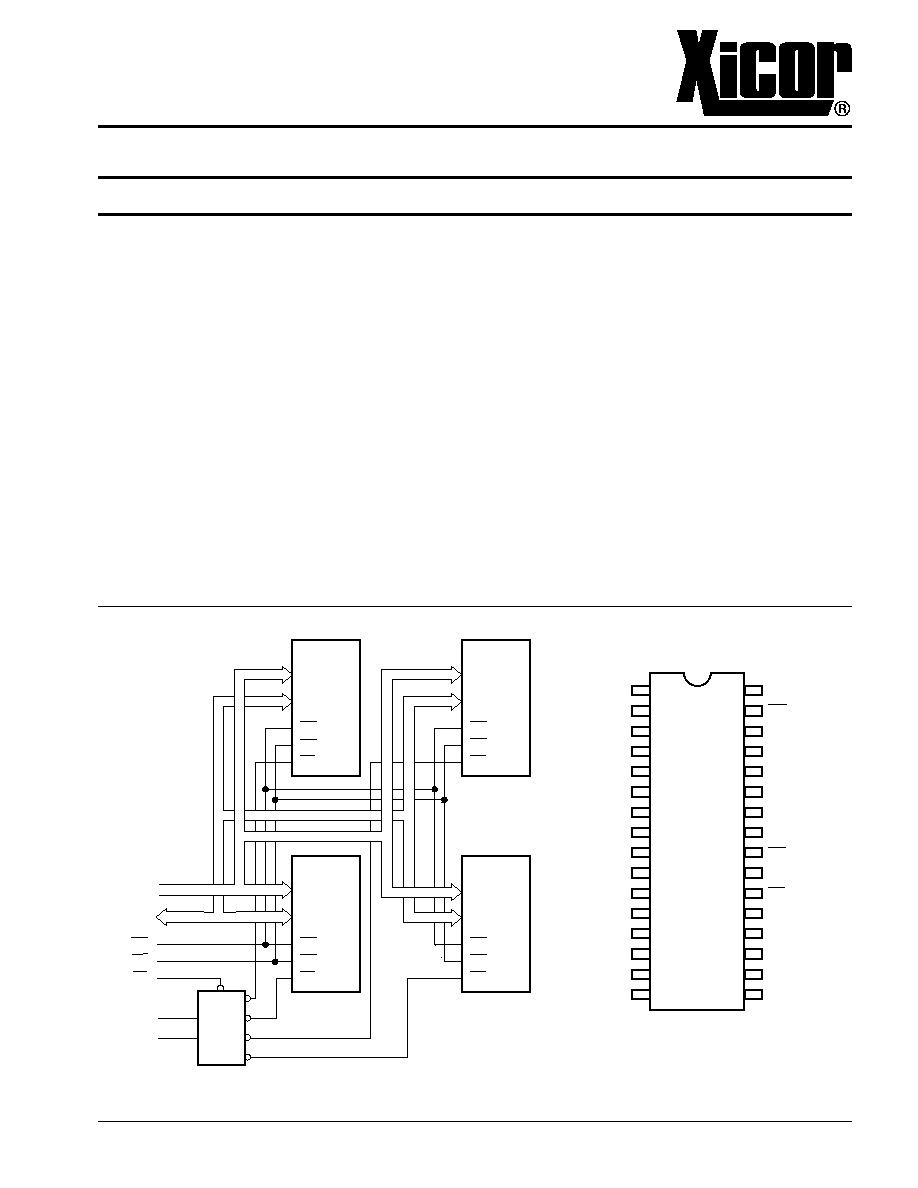
The XM28C040 is a high density 4 Megabit E
2
PROM
comprised of four X28C010's mounted on a co-fired
multilayered ceramic substrate. Individual components
are 100% tested prior to assembly in module form and
then 100% tested after assembly.
The XM28C040 is configured 512K x 8 bit. The module
supports a 256-byte page write operation. This com-
bined with
DATA
Polling or Toggle Bit Polling, effectively
provides a 39
µ
s/byte write cycle, enabling the entire
array to be rewritten in 10 seconds.
The XM28C040 provides the same high endurance and
data retention as the X28C010.
4 Megabit Module
XM28C040
512K x 8 Bit
3873 FHD F01
WE
OE
CE
A18
A17
I/O0≠I/O7
A0≠A16
X28C010
A0≠A16
I/O0≠I/O7
CE
WE
OE
OE
X28C010
A0≠A16
I/O0≠I/O7
CE
WE
X28C010
A0≠A16
I/O0≠I/O7
CE
WE
OE
X28C010
A0≠A16
I/O0≠I/O7
CE
WE
OE
FUNCTIONAL DIAGRAM
PIN CONFIGURATION
3873 FHD F02
A18
A16
A15
A12
A7
A6
A5
A4
A3
A2
A1
A0
I/O0
I/O1
I/O2
VSS
1
2
3
4
5
6
7
8
9
10
11
12
13
14
15
16
32
31
30
29
28
27
26
25
24
23
22
21
20
19
18
17
VCC
WE
A17
A14
A13
A8
A9
A11
OE
A10
CE
I/O7
I/O6
I/O5
I/04
I/O3
XM28C040

XM28C040
2
PIN DESCRIPTIONS
Addresses (A
0
≠A
18
)
The Address inputs select an 8-bit memory location
during a read or write operation.
Chip Enable (
CE
)
The Chip Enable input must be LOW to enable all read/
write operations. When
CE
is HIGH, power consumption
is reduced (see Note 4).
Output Enable (
OE
)
The Output Enable input controls the data output buffers
and is used to initiate read operations.
Data In/Data Out (I/O
0
≠I/O
7
)
Data is written to or read from the XM28C040 through
the I/O pins.
Write Enable (
WE
)
The Write Enable input controls the writing of data to the
XM28C040.
PIN NAMES
Symbol
Description
A
0
≠A
18
Address Inputs
I/O
0
≠I/O
8
Data Input/Output
WE
Write Enable
CE
Chip Enable
OE
Output Enable
V
CC
+5V
V
SS
Ground
NC
No Connect
3873 PGM T01
XM28C040
3
DEVICE OPERATION
Read
Read operations are initiated by both
OE
and
CE
LOW.
The read operation is terminated by either
CE
or
OE
returning HIGH. This 2-line control architecture elimi-
nates bus contention in a system environment. The data
bus will be in a high impedance state when either
OE
or
CE
is HIGH.
Write
Write operations are initiated when both
CE
and
WE
are
LOW and
OE
is HIGH. The XM28C040 supports both a
CE
and
WE
controlled write cycle. That is, the address
is latched by the falling edge of either
CE
or
WE
,
whichever occurs last. Similarly, the data is latched
internally by the rising edge of either
CE
or
WE
, which-
ever occurs first. A byte write operation, once initiated,
will automatically continue to completion, typically within
5ms (see Note 4).
Page Write Operation
The page write feature of the XM28C040 allows the
entire memory to be written in 10 seconds. Page write
allows two to 256 bytes of data to be consecutively
written to the XM28C040 prior to the commencement of
the internal programming cycle. The host can fetch data
from another device within the system during a page
write operation (change the source address), but the
page address (A
8
through A
18
) for each subsequent
valid write cycle to the part during this operation must be
the same as the initial page address.
The page write mode can be initiated during any write
operation. Following the initial byte write cycle, the host
can write an additional one to 255 bytes in the same
manner as the first byte was written. Each successive
byte load cycle, started by the
WE
HIGH to LOW
transition, must begin within 100
µ
s of the falling edge of
the preceding
WE
. If a subsequent
WE
HIGH to LOW
transition is not detected within 100
µ
s, the internal
automatic programming cycle will commence. There is
no page write window limitation. Effectively the page
write window is infinitely wide, so long as the host
continues to access the device within the byte load cycle
time of 100
µ
s.
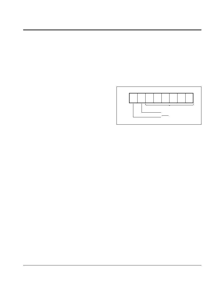
Write Operation Status Bits
The XM28C040 provides the user two write operation
status bits. These can be used to optimize a system
write cycle time. The status bits are mapped onto the
I/O bus as shown in Figure 1.
DATA
Polling (I/O
7
)
Figure 1. Status Bit Assignment
The XM28C040 features
DATA
Polling as a method to
indicate to the host system that the byte write or page
write cycle has completed.
DATA
Polling allows a simple
bit test operation to determine the status of the
XM28C040, eliminating additional interrupt inputs or
external hardware. During the internal programming
cycle, any attempt to read the last byte written will
produce the complement of that data on I/O
7
(i.e., write
data = 0xxx xxxx, read data = 1xxx xxxx). Once the
programming cycle is complete, I/O
7
will reflect true
data. Note: If the XM28C040 is in the protected state and
an illegal write operation is attempted,
DATA
Polling will
not operate.
Toggle Bit (I/O
6
)
The XM28C040 also provides another method for deter-
mining when the internal write cycle is complete. During
the internal programming cycle I/O
6
will toggle from "1"
to "0" and "0" to "1" on subsequent attempts to read the
last byte written. When the internal cycle is complete the
toggling will cease and the device will be accessible for
additional read or write operations.
3873 FHD F09
5
TB
DP
4
3
2
1
0
I/O
RESERVED
TOGGLE BIT
DATA POLLING
XM28C040
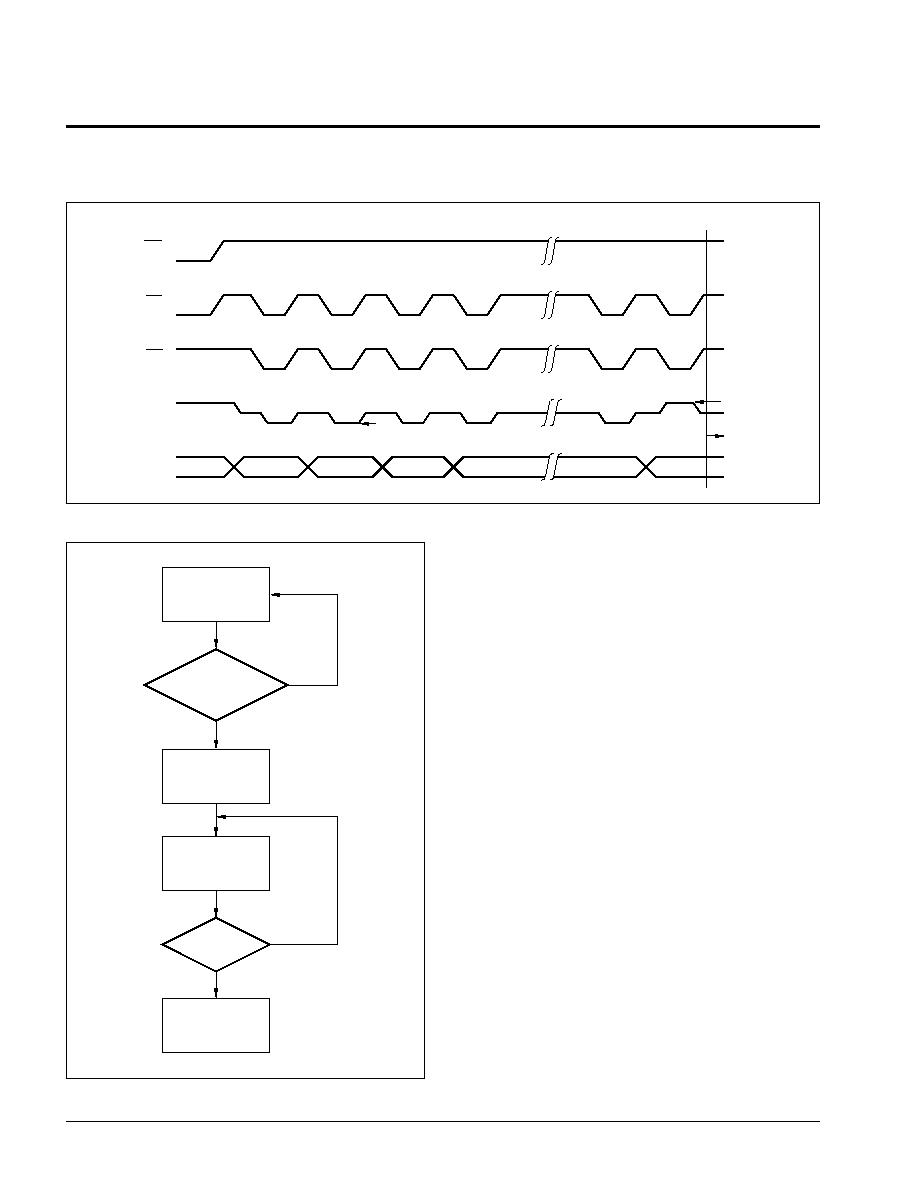
4
DATA
POLLING I/O
7
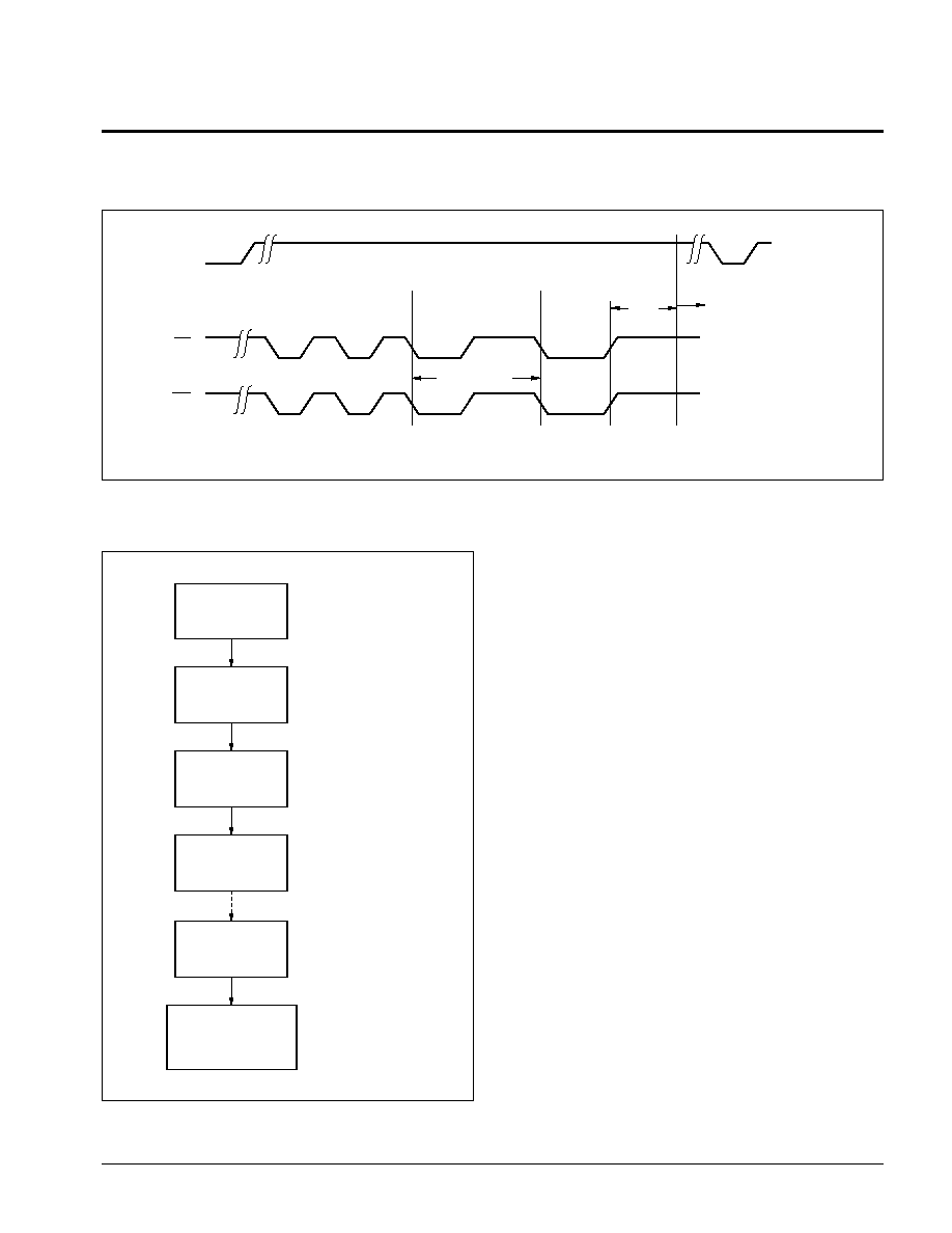
Figure 2.
DATA
Polling Bus Sequence
Figure 3.
DATA
Polling Software Flow
DATA
Polling can effectively halve the time for writing to
the XM28C040. The timing diagram in Figure 2 illus-
trates the sequence of events on the bus. The software
flow diagram in Figure 3 illustrates one method of
implementing the routine.
3873 FHD F10
3873 FHD F11
CE
OE
WE
I/O7
READY
LAST
WRITE
HIGH Z
VOL
VIH
A0≠A18
An
An
An
An
An
An
VOH
An
WRITE DATA
SAVE LAST DATA
AND ADDRESS
READ LAST
ADDRESS
IO7
COMPARE?
READY
NO
YES
WRITES
COMPLETE?
NO
YES
XM28C040
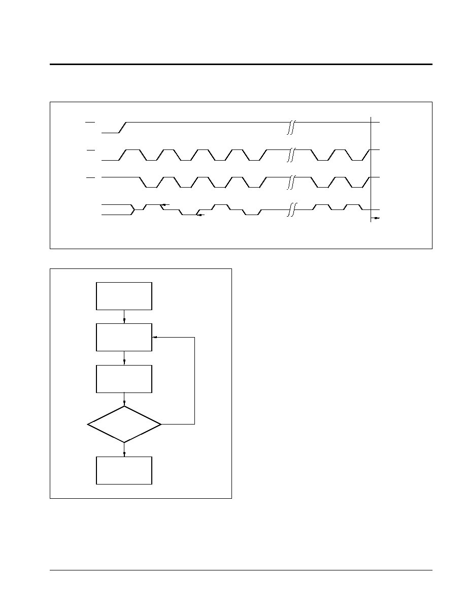
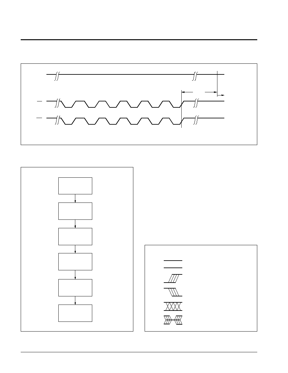
5
THE TOGGLE BIT I/O
6
Figure 4. Toggle Bit Bus Sequence
Figure 5. Toggle Bit Software Flow
The Toggle Bit can eliminate the software housekeeping
chore of saving and fetching the last address and data
written to a device in order to implement
DATA
Polling.
This can be especially helpful in an array comprised of
multiple XM28C040 memories that is frequently up-
dated. The timing diagram in Figure 4 illustrates the
sequence of events on the bus. The software flow
diagram in Figure 5 illustrates a method for testing the
Toggle Bit.
3873 FHD F12
3873 FHD F13
CE
OE
WE
I/O6
READY
VOH
VOL
LAST
WRITE
HIGH Z
* Beginning and ending state of I/O6 will vary.
*
*
LOAD ACCUM
FROM ADDR n
COMPARE
ACCUM WITH
ADDR n
READY
COMPARE
OK?
NO
YES
LAST WRITE

XM28C040
6
memory ICs and decoder should be considered memory
board components and SDP can be implemented at the
component level as described in the next section.
SOFTWARE COMMAND SEQUENCE
A
17
and A
18
are used by the decoder to select one of the
four LCCs. Therefore, only one of the four memory
devices can be accessed at one time. In order to protect
the entire module, the command sequence must be
issued separately to each device.
Enabling the software data protection mode requires the
host system to issue a series of three write operations:
each write operation must conform to the data and
address sequence illustrated in Figures 6 and 7.
Because this involves writing to a nonvolatile bit, the
device will become protected after t
WC
has elapsed.
After this point in time devices will inhibit inadvertent
write operations.
Once in the protected mode, authorized writes may be
performed by issuing the same command sequence that
enables SDP, immediately followed by the address/data
combination desired. The command sequence opens
the page write window enabling the host to write from
one to 256 bytes of data. Once the data has been
written, the device will automatically be returned to the
protected state.
In order to facilitate testing of the devices the SDP mode
can be deactivated. This is accomplished by issuing a
series of six write operations: each write operation must
conform to the data and address sequence illustrated in
Figures 8 and 9. This is a nonvolatile operation, and the
host will have to wait a minimum t
WC
before attempting
to write new data.
HARDWARE DATA PROTECTION
The XM28C040 provides three hardware features that
protect nonvolatile data from inadvertent writes.
∑ Noise Protection--A
WE
pulse less than 10ns will not
initiate a write cycle.
∑ Default V
CC
Sense--All functions are inhibited when
V
CC
is
3V.
∑ Write Inhibit--Holding
OE
LOW will prevent an inad-
vertent write cycle during power-up and power-down.
SOFTWARE DATA PROTECTION
The XM28C040 does provide the Software Data Protec-
tion (SDP) feature.
The module is shipped from Xicor with the Software
Data Protection NOT ENABLED; that is, the module will
be in the standard operating mode. In this mode, data
should be protected during power-up/-down operations
through the use of external circuits. The host system will
then have open read and write access of the module
once V
CC
is stable.
The module can be automatically protected during power-
up/-down without the need for external circuits by em-
ploying the SDP feature. The internal SDP circuit is
enabled after the first write operation utilizing the SDP
command sequence.
When this feature is employed, it will be easiest to
incorporate in the system software if the module is
viewed as a subsystem composed of four discrete
memory devices with an address decoder (see Func-
tional Diagram). In this manner, system memory map-
ping will extend onto the module. That is, the discrete
XM28C040
7
SOFTWARE DATA PROTECTION
Figure 6. Timing Sequence--Byte or Page Write
3873 FHD F14
Figure 7. Write Sequence for
Software Data Protection
Regardless of whether the device has previously been
protected or not, once the software data protected
algorithm is used and data has been written, the device
will automatically disable further writes unless another
command is issued to cancel it. If no further commands
are issued the device will be write protected during
power-down and after any subsequent power-up.
3873 FHD F15
WRITE LAST
BYTE TO
LAST ADDRESS
WRITE DATA 55
TO ADDRESS
2AAA
WRITE DATA A0
TO ADDRESS
5555
WRITE DATA XX
TO ANY
ADDRESS
AFTER tWC
RE-ENTERS DATA
PROTECTED STATE
WRITE DATA AA
TO ADDRESS
5555
BYTE/PAGE
LOAD ENABLED
CE
WE
(VCC)
WRITE
PROTECTED
VCC
0V
DATA
ADDR.
A0≠A16*
AA
5555
55
2AAA
A0
5555
tBLC MAX
WRITES
OK
BYTE
OR
PAGE
*A17 & A18 select one of four devices on the module.
tWC
XM28C040
8
RESETTING SOFTWARE DATA PROTECTION
Figure 8. Reset Software Data Protection Timing Sequence
3873 FHD F16
3873 FHD F17
Figure 9. Software Sequence to Deactivate
Software Data Protection
In the event the user wants to deactivate the software
data protection feature for testing or reprogramming in
an E
2
PROM programmer, the following six step algo-
rithm will reset the internal protection circuit. After t
WC
,
the device will be in standard operating mode.
WRITE DATA 55
TO ADDRESS
2AAA
WRITE DATA 55
TO ADDRESS
2AAA
WRITE DATA 80
TO ADDRESS
5555
WRITE DATA AA
TO ADDRESS
5555
WRITE DATA 20
TO ADDRESS
5555
WRITE DATA AA
TO ADDRESS
5555
CE
WE
STANDARD
OPERATING
MODE
VCC
DATA
ADDR.
A0≠A16*
AA
5555
55
2AAA
80
5555
*A17 & A18 select one of four devices on the module.
tWC
AA
5555
55
2AAA
20
5555
WAVEFORM
INPUTS
OUTPUTS
Must be
steady
Will be
steady
May change
from LOW
to HIGH
Will change
from LOW
to HIGH
May change
from HIGH
to LOW
Will change
from HIGH
to LOW
Don't Care:
Changes
Allowed
Changing:
State Not
Known
N/A
Center Line
is High
Impedance
SYMBOL TABLE

XM28C040
9
SYSTEM CONSIDERATIONS
Because the XM28C040 is frequently used in large
memory arrays it is provided with a two line control
architecture for both read and write operations. Proper
usage can provide the lowest possible power dissipation
and eliminate the possibility of contention where mul-
tiple I/O pins share the same bus.
To gain the most benefit it is recommended that
CE
be
decoded from the address bus and be used as the
primary device selection input. Both
OE
and
WE
would
then be common among all devices in the array. For a
read operation this assures that all deselected devices
are in their standby mode and that only the selected
device(s) is outputting data on the bus.
Because the XM28C040 has two power modes, standby
and active, proper decoupling of the memory array is of
prime concern. Enabling
CE
will cause transient current
spikes. The magnitude of these spikes is dependent on
the output capacitive loading of the I/Os. Therefore, the
larger the array sharing a common bus, the larger the
transient spikes. The voltage peaks associated with the
current transients can be suppressed by the proper
selection and placement of decoupling capacitors. As a
minimum, it is recommended that a 0.1
µ
F high fre-
quency ceramic capacitor be used between V
CC
and
V
SS
at each device. Depending on the size of the array,
the value of the capacitor may have to be larger.
In addition, it is recommended that a 4.7
µ
F electrolytic
bulk capacitor be place between V
CC
and V
SS
for every
two modules employed in the array. This bulk capacitor
is employed to overcome the voltage droop caused by
the inductive effects of the PC board traces.
XM28C040
10
ABSOLUTE MAXIMUM RATINGS*
Temperature under Bias .................. ≠65
∞
C to +135
∞
C
Storage Temperature ....................... ≠65
∞
C to +150
∞
C
Voltage on any Pin with
Respect to V
SS ................................................
≠1V to +7V
D.C. Output Current ............................................. 5mA
Lead Temperature
(Soldering, 10 seconds) .............................. 300
∞
C
*COMMENT
Stresses above those listed under "Absolute Maximum
Ratings" may cause permanent damage to the device.
This is a stress rating only and the functional operation of
the device at these or any other conditions above those
indicated in the operational sections of this specification is
not implied. Exposure to absolute maximum rating condi-
tions for extended periods may affect device reliability.
D.C. OPERATING CHARACTERISTICS
XM28C040 T
A
= 0
∞
C to +70
∞
C, V
CC
= +5V
±
10%, unless otherwise specified.
XM28C040I T
A
= ≠40
∞
C to +85
∞
C, V
CC
= +5V
±
10%, unless otherwise specified.
XM28C040M T
A
= ≠55
∞
C to +125
∞
C, V
CC
= +5V
±
10%, unless otherwise specified.
Limits
Symbol
Parameter
Min.
Max.
Units
Test Conditions
I
CC
V
CC
Current (Active)
80
mA
CE
=
OE
= V
IL
,
WE
= V
IH
,
(TTL Inputs)
All I/O's = Open, 1 Device Active
Address Inputs = TTL Levels
@ f = 5MHz
I
SB
V
CC
Current (Standby)
5
mA
CE
, A
17
, A
18
= V
CC
≠0.3V
All other inputs = V
IH
All I/Os = OPEN
I
LI
Input Leakage Current
10
µ
A
V
IN
= V
SS
to V
CC
I
LO
Output Leakage Current
10
µ
A
V
OUT
= V
SS
to V
CC
,
CE
= V
IH
V
lL
Input LOW Voltage
≠1
0.8
V
V
IH
Input HIGH Voltage
2
V
CC
+ 1
V
V
OL
Output LOW Voltage
0.4
V
I
OL
= 2.1mA
V
OH
Output HIGH Voltage
2.4
V
I
OH
= ≠400
µ
A
3873 PGM T02.2
POWER-UP TIMING
Symbol
Parameter
Typ.
(1)
Units
t
PUR
(2)
Power-up to Initiation of Read Operation
100
ms
t
PUW
(2)
Power-up to Initiation of Write Operation
5
ms
3873 PGM T03
CAPACITANCE T
A
= +25
∞
C, f = 1MHz, V
CC
= 5V
Symbol
Parameter
Max.
Units
Test Conditions
C
I/O
(2)
Input/Output Capacitance
50
pF
V
I/O
= 0V
C
IN
(2)
Input Capacitance
50
pF
V
IN
= 0V
3873 PGM T04.1
Notes: (1) Typical values are for T
A
= 25
∞
C and nominal supply voltage.
(2) This parameter is periodically sampled and not 100% tested.
XM28C040
11
Note: (3)
t
HZ
and t
OHZ
are measured from the point when
CE
or
OE
return high (whichever occurs first) to the time when the outputs are
no longer driven.
3873 FHD F03
MODE SELECTION
CE
OE WE
Mode
I/O
Power
L
L
H
Read
D
OUT
Active
L
H
L
Write
D
IN
Active
H
X
X
Standby and Write Inhibit
High Z
Standby
X
L
X
Write Inhibit
--
--
X
X
H
Write Inhibit
--
--
3873 PGM T06
A.C. CHARACTERISTICS
XM28C040 T
A
= 0
∞
C to +75
∞
C, V
CC
= +5V
±
10%, unless otherwise specified.
XM28C040I T
A
= ≠40
∞
C to +85
∞
C, V
CC
= +5V
±
10%, unless otherwise specified.
XM28C040M T
A
= ≠55
∞
C to +125
∞
C, V
CC
= +5V
±
10%, unless otherwise specified.
Read Cycle Limits
XM28C040-20
XM28C040-25
XM28C040
Symbol
Parameter
Min.
Max.
Min.
Max.
Min.
Max.
Units
t
RC
Read Cycle Time
200
250
300
ns
t
CE
Chip Enable Access Time
200
250
300
ns
t
AA
Address Access Time
200
250
300
ns
t
OE
Output Enable Access Time
80
100
100
ns
t
LZ
(4)
CE
Low to Active Output
0
0
0
ns
t
OLZ
(4)
OE
Low to Active Output
0
0
0
ns
t
HZ
(4)
CE
High to High Z Output
100
100
100
ns
t
OHZ
(4)
OE
High to High Z Output
100
100
100
ns
t
OH
Output Hold From Address Change
0
0
0
ns
3873 PGM T07
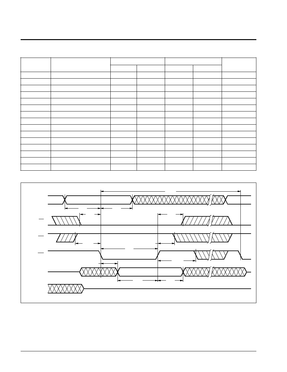
Read Cycle
tCE
tRC
ADDRESS
CE
OE
WE
DATA VALID
DATA VALID
tOE
tLZ
tOLZ
tOH
tAA
tHZ
tOHZ
DATA I/O
VIH
HIGH Z
A.C. CONDITIONS OF TEST
Input Pulse Levels
0V to 3V
Input Rise and
Fall Times
10ns
Input and Output
Timing Levels
1.5V
Output Load
1 TTL Gate and
C
L
= 100pF
3873 PGM T05.1
XM28C040
12
Write Cycle Limits
WE
Controlled Write
CE
Controlled Write
(4)
Symbol
Parameter
Min.
Max.
Min.
Max.
Units
t
WC
Write Cycle Time
10
10
ms
t
AS
Address Setup Time
0
0
ns
t
AH
Address Hold Time
125
125
ns
t
CS
Write Setup Time
25
0
ns
t
CH
Write Hold Time
0
25
ns
t
CW
CE
Pulse Width
125
100
ns
t
OES
OE
High Setup Time
10
10
ns
t
OEH
OE
High Hold Time
10
35
ns
t
WP
WE
Pulse Width
100
125
ns
t
WPH
WE
High Recovery
100
100
ns
t
DV
Data Valid
1
1
µ
s
t
DS
Data Setup
50
50
ns
t
DH
Data Hold
10
35
ns
t
DW
Delay to Next Write
10
10
µ
s
t
BLC
Byte Load Cycle
0.3
100
0.3
100
µ
s
3873 PGM T08.1
WE
Controlled Write Cycle
3873 FHD F04
Note: (4) Due to the inclusion of the decoder IC on board the module the
WE
and
CE
write controlled timings will vary. When utilizing the
CE
controlled write operation all the hold timings must be extended by the worst case propagation delay of the decoder. For a
WE
controlled write operation
CE
must be a minimum 125ns to accommodate the additional setup time required.
ADDRESS
tAS
tWC
tAH
tOES
tDV
tDS
tOEH
CE
WE
OE
DATA IN
DATA OUT
HIGH Z
DATA VALID
tCS
tCH
tWP
tWPH
tDH
XM28C040
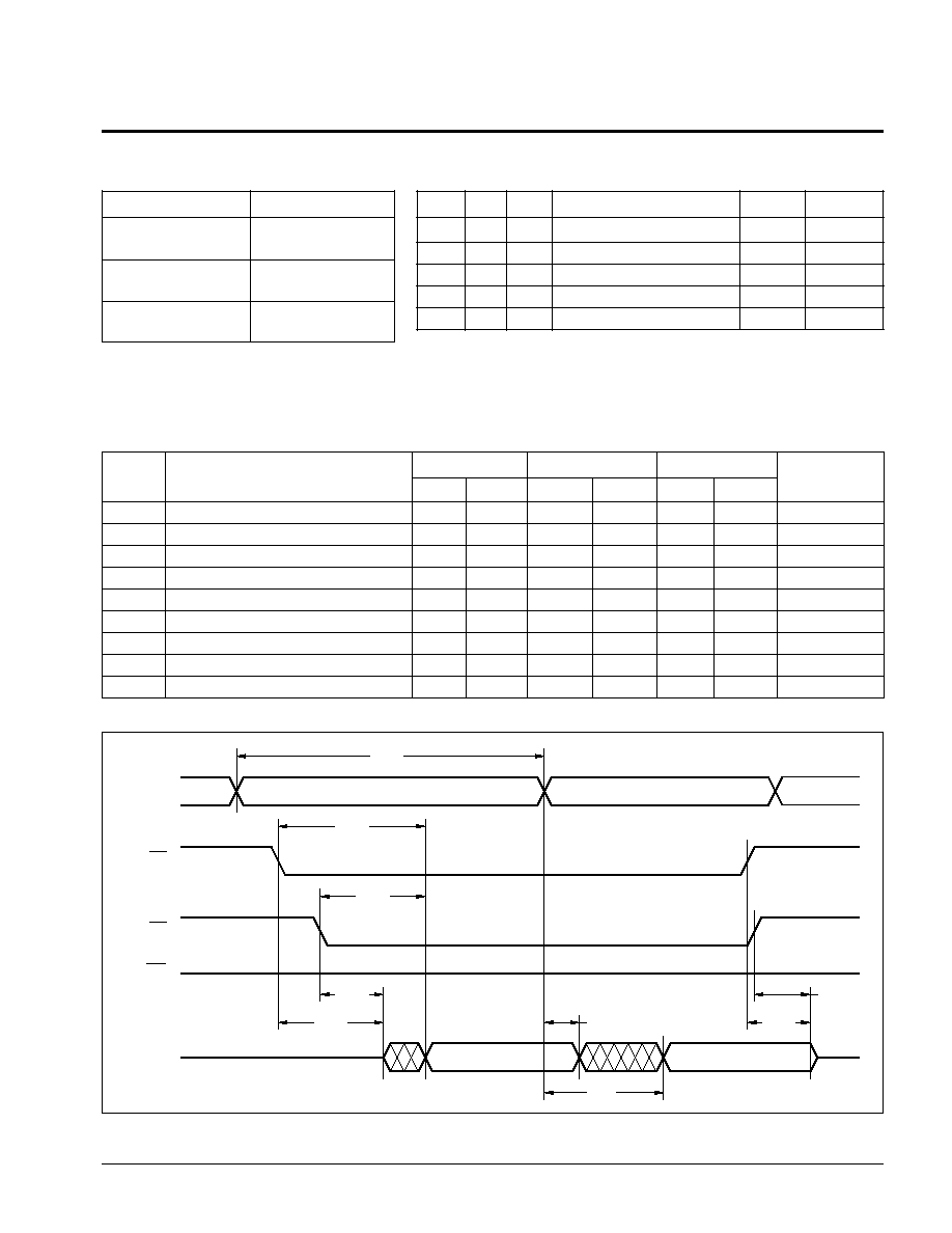
13
CE
Controlled Write Cycle
3873 FHD F05
Page Write Cycle
3873 FHD F06
ADDRESS
tAS
tOEH
tWC
tAH
tOES
tWPH
tCS
tDV
tDS
tDH
tCH
CE
WE
OE
DATA IN
DATA OUT
HIGH Z
DATA VALID
tCW
WE
OE
BYTE 0
BYTE 1
BYTE 2
BYTE n
BYTE n+1
BYTE n+2
tWP
tWPH
tBLC
tWC
CE
*ADDRESS
I/O
*For each successive write within the page write operation, A7≠A18 should be the same or
writes to an unknown address could occur.
LAST BYTE
XM28C040
14
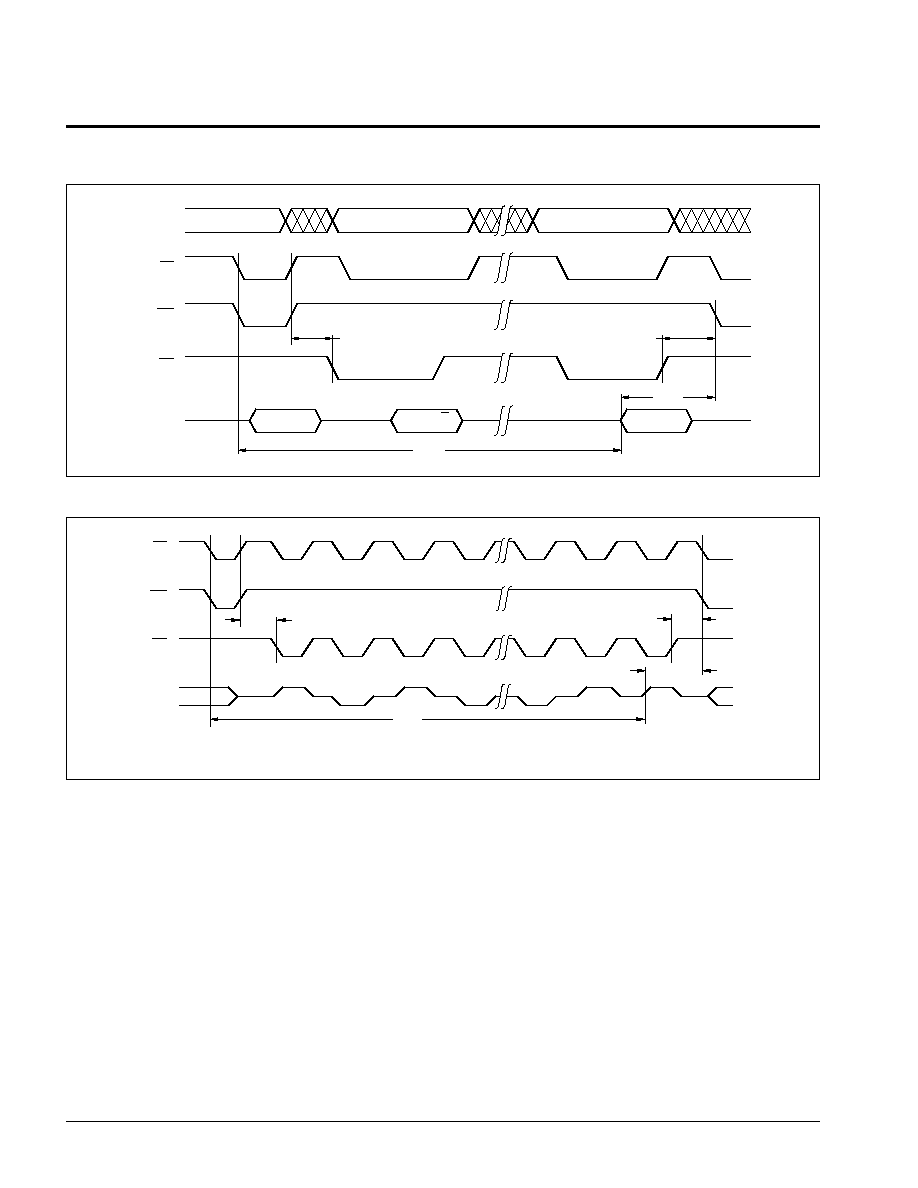
DATA
Polling Timing Diagram
ADDRESS
An
DIN=X
DOUT=X
DOUT=X
tWC
tOEH
tOES
CE
WE
OE
I/O7
tDW
An
An
Toggle Bit Timing Diagram
CE
OE
WE
I/O6
tOES
tDW
tWC
tOEH
HIGH Z
*
*
* Starting and ending state of I/O6 will vary, depending upon actual tWC.
3873 FHD F07
3873 FHD F08
XM28C040
15
MultiPlane Architecture
The design of the XM28C040 has implemented a mul-
tiplane architecture. That is, there are four independent
128K x 8 memory spaces or planes, each selected by its
own chip enable input via the on-board decoder chip.
This architecture can be utilized in a number of ways.
Separate Data and Program Memory Spaces
The multiplane concept allows the system to write to one
plane of the module and still be able to read (continue
executing code) from the module, utilizing any plane not
performing a write operation.
This concept of separate data and program spaces can
be expanded by providing a simple off-module circuit
that will disable writes to predetermined portions of
memory. A very basic version is shown in the Functional
Diagram. Whenever A
18
is HIGH, the
WE
input is forced
HIGH, write protecting one half the module. This half
would be reserved for read only program store while the
other half would be available for read and write data
store.
Expanded Sequential Page Lengths
A standard system implementation would be decoding
externally the module's chip enable and then wiring
each address of the module to its corresponding ad-
dress line in the system. This would effectively provide
the system a memory organized as four separate memory
planes with a sequential page address space of 256
bytes.
In an application such as data logging, the most efficient
method of logging the data is in a sequential manner. If
the data come in bursts that exceed 256 bytes in length
a longer page might be desirable. By swapping address
lines externally the effective page length can be ex-
panded to 1024 bytes. Refer to the table below for a
matrix illustrating the various page length options.
TABLE 1. ADDRESS TRANSLATION MATRIX
Effective
A
0
-A
7
A
8
-A
16
A17
A
18
Page Size
No. of
Planes
A0-A7
A8-A16
A17
A18
256
4
A0-A7
A9-A17
A8
A18
512
2
A0-A7
A10-A18
A8
A9
1024
1
3873 PGM T09
System
Address
Lines
Module Address Inputs
Note:
The user should be aware the overall I
CC
of the module will increase as more individual components on the module are activated.
XM28C040
16
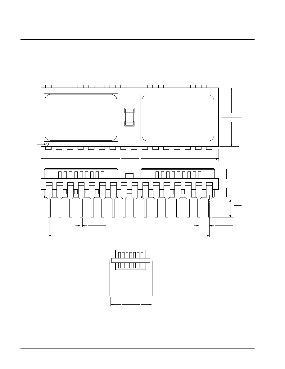
PACKAGING INFORMATION
1.610 (40.89)
1.590 (40.39)
PIN 1
1.508 (38.30)
1.492 (37.90)
TOL. NON. ACCUM.
0.020 (0.51)
0.016 (0.41)
.100
±
.005
(2.54
±
.13)
TYP.
0.300
(7.62)
MAX.
.125
(3.18)
MIN.
0.604 (15.34)
0.596 (15.14)
3926 ILL F47
32-PIN DUAL-IN-LINE MODULE USING
STRETCHED CERAMIC LEADLESS CHIP CARRIERS
ON SIDE BRAZED CERAMIC SUBSTRATE
NOTES:
1. ALL DIMENSIONS IN INCHES (IN PARENTHESES IN MILLIMETERS)
2. DIMENSIONS WITH NO TOLERANCE FOR REFERENCE ONLY
0.610 (15.49)
0.590 (14.99)
XM28C040
17
ORDERING INFORMATION
XM28C040: 512K X 8 CMOS E
2
PROM Module
Access Time
≠20 = 200ns
≠25 = 250ns
Blank = 300ns
Temperature Range
Blank = Commercial = 0
∞
C to +70
∞
C
I = Industrial = ≠40
∞
C to +85
∞
C
M = Military = ≠55
∞
C to +125
∞
C
MHR = Military High Rel
Blank = 32-Lead Ceramic Module
XM28C040 X
X
-X
Device
LIMITED WARRANTY
Devices sold by Xicor, Inc. are covered by the warranty and patent indemnification provisions appearing in its Terms of Sale only. Xicor, Inc. makes no warranty,
express, statutory, implied, or by description regarding the information set forth herein or regarding the freedom of the described devices from patent infringement.
Xicor, Inc. makes no warranty of merchantability or fitness for any purpose. Xicor, Inc. reserves the right to discontinue production and change specifications and
prices at any time and without notice.
Xicor, Inc. assumes no responsibility for the use of any circuitry other than circuitry embodied in a Xicor, Inc. product. No other circuits, patents, licenses are
implied.
U.S. PATENTS
Xicor products are covered by one or more of the following U.S. Patents: 4,263,664; 4,274,012; 4,300,212; 4,314,265; 4,326,134; 4,393,481; 4,404,475;
4,450,402; 4,486,769; 4,488,060; 4,520,461; 4,533,846; 4,599,706; 4,617,652; 4,668,932; 4,752,912; 4,829, 482; 4,874, 967; 4,883, 976. Foreign patents and
additional patents pending.
LIFE RELATED POLICY
In situations where semiconductor component failure may endanger life, system designers using this product should design the system with appropriate error
detection and correction, redundancy and back-up features to prevent such an occurence.
Xicor's products are not authorized for use in critical components in life support devices or systems.
1. Life support devices or systems are devices or systems which, (a) are intended for surgical implant into the body, or (b) support or sustain life, and whose
failure to perform, when properly used in accordance with instructions for use provided in the labeling, can be reasonably expected to result in a significant
injury to the user.
2. A critical component is any component of a life support device or system whose failure to perform can be reasonably expected to cause the failure of the life
support device or system, or to affect its safety or effectiveness.