 | –≠–ª–µ–∫—Ç—Ä–æ–Ω–Ω—ã–π –∫–æ–º–ø–æ–Ω–µ–Ω—Ç: C8259A | –°–∫–∞—á–∞—Ç—å:  PDF PDF  ZIP ZIP |
December 6, 2001
1
CAST, Inc.
11 Stonewall Court
Woodcliff Lake, New Jersey 07677 USA
Phone:
201-391-8300
Fax:
201-391-8694
E-Mail:
info@cast-inc.com
URL:
www.cast-inc.com
Features
∑
Available under terms of the SignOnce IP License
∑
Eight vectored priority interrupts per core. Up to sixty-
four vectored priority interrupts with cascading
∑
Programming for all 8259A modes and operational
features:
-
MCS-80/85 and 8088/8086 processor modes
-
Fully nested mode and special fully nested mode
-
Special mask mode
-
Buffered mode
-
Pool command mode
-
Cascade mode with master or slave selection
-
Automatic end-of-interrupt mode
-
Specific and non-specific end-of-interrupt
commands
-
Automatic Rotation
-
Specific Rotation
-
Edge and level triggered interrupt input modes
-
Reading of interrupt request register (IRR) and in-
service register (ISR) through data bus
-
Writing and reading of interrupt mask register (IMR)
through data bus
∑
Functionally based on the Intel 8259A and Harris
82C59A devices
Applications
The C8259A core is used in real time, interrupt driven
microcomputer designs.
AllianceCORETM Facts
Core Specifics
See Table 1
Provided with Core
Documentation
Core documentation
Design File Formats
.ngo, EDIF Netlist,
VHDL Source RTL available extra
Constraints File
C8259A.ucf
Verification
VHDL testbench, test vectors
Instantiation
Templates
None
Reference designs &
application notes
None
Additional Items
None
Simulation Tool Used
1076 compliant VHDL simulator, Verilog simulator
Support
Support provided by CAST, Inc.
Table 1: Core Implementation Data
Supported
Family
Device
Tested
CLB
Slices
2
Clock
IOBs
1
IOBs
1
Performance
(MHz)
Xilinx
Tools
Special
Features
Virtex-II
XC2V40-5
230
2
25
142
ISE4.1i
None
Virtex-E
XCV50E-8
215
2
25
58
M2.1i
None
Virtex
XCV50-6
215
2
25
49
M2.1i
None
Spartan-II
XC2S50-6
215
2
25
47
M2.1i
None
Notes:
1. Assuming all core I/Os are routed off-chip.
2. Optimized for speed.
C8259A Programmable Interrupt
Controller
December 6, 2001
Product Specification
C8259A Programmable Interrupt Controller
2
December 6, 2001
General Description
The C8259A Programmable Interrupt Controller core man-
ages up to 8 vectored priority interrupts for a processor.
Using multiple instantiations of the core and programming it
to cascade mode allows for up to sixty-four vectored inter-
rupts. More than sixty-four vectored interrupts can be
accomplished by programming the core to Poll Command
Mode.
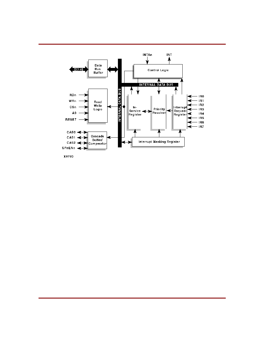
Functional Description
The C8259A core is partitioned into modules as shown in
Figure 1 and described below.
Data Bus Buffer
This 3-state, bi-directional 8-bit buffer is used to interface
the C8259A core to the system Data Bus. Control words
and status information are transferred through the Data
Bus Buffer.
Read / Write Logic
The function of this block is to accept output commands
from the CPU. It contains the initialization Command Word
(ICW) registers and Operation Command Word (OCW)
registers which store the various control formats for device
operation. The Read/Write Logic block also allows the sta-
tus of the C8259A core to be transferred onto the Data Bus.
Cascade Buffer Comparator
This block stores and compares the Ids of all C8259A's
used in the system. The associated three I/O pins (CAS0-
2) are outputs when the C8259A is used as a master and
are inputs when the C8259A is used as a slave. As a mas-
ter, the C8259A core sends the ID of the interrupting slave
device onto the CAS0-2 lines. The selected slave will send
its preprogrammed subroutine address onto the Data Bus
during the next one or two consecutive INTAn pulses.
Control Logic
This block checks for INTAn pulses which cause the
C8259A to release vectoring information onto the Data
Bus. The format of this data depends on the system mode
of the C8259A. This block also sets the interrupt output
high whenever a valid interrupt request is asserted.
Interrupt Request Register (IRR) and In-
Service Register (ISR)
The interrupts at the IR input lines are handled by two reg-
isters in tandem, the Interrupt Request Register (IRR) and
the In-Service Register (ISR). The IRR is used to store all
Figure 1: C8259A Programmable Interrupt Controller Block Diagram

December 6, 2001
3
CAST, Inc.
the interrupt levels which are requesting service. The ISR is
used to store all the interrupt levels that are being serviced.
Priority Resolver
This block determines the priorities of the bits set in the
IRR. The highest priority is selected and strobed into the
corresponding bit of the ISR during an INTAn pulse.
Interrupt Masking Register (IMR)
The IMR stores the bits that control the interrupt lines to be
masked. The IMR operates on the IRR. Masking of a higher
priority input will not affect the interrupt request lines of
lower priority.
Pinout
The pinout of the C8259A core has not been fixed to spe-
cific FPGA I/O, allowing flexibility with a users application.
Signal names are shown in the block diagram in Figure 1
and described in Table 2.
Table 2: Core Signal Pinout
Core Modifications
The C8259A core can be customized to include a greater
number of interrupts. Please contact CAST, Inc. directly for
any required modifications.
Core Assumptions
Power-up RESET Input
Due to an inadequate amount of I/O pins on the original
Intel 8259A device, a reset capability was not included. The
Intel 8259A and the Harris 82C59A reset when Initialize
Command Word 1 (ICW1) is written to the device.
The C8259A model contains a RESET signal in its top-level
entity. RESET will force the simulation or synthesized cir-
cuit into a known state, equivalent to when ICW1 is written.
Note that whenever ICW1 is written, the model resets con-
forming to the Intel and Harris specifications.
Rotate in Automatic EOI Mode
In the Intel 8259A, when Rotate in Automatic EOI Mode is
set, and a DEFAULT IR7 (spurious noise glitch on any of
the IR inputs) occurs, the priority of pending interrupts will
still rotate. This is not a serious problem since subsequent
interrupts will in fact be serviced, but in a different order
than originally intended.
In the C8259A model, however, this feature was not imple-
mented. A DEFAULT IR7 will not cause a Rotation in the
interrupt priority.
Interrupt Acknowledge
During the first INTAn strobe of an Interrupt Acknowledge
Cycle, the Intel 8259A sets the highest priority ISR bit using
the leading edge of INTAn.
In the C8259A model, the highest priority ISR bit is set on
the first INTAn's rising edge (at the end of the first INTAn
cycle). Functionally, both the Intel 8259A and the C8259A
models are identical: the model freezes all pending IRR bits
with INTAn's falling edge. By actually setting the ISR at the
end of the INTAn cycle, the model has the pulse width of
INTAn to allow for the IRR bits to settle within the synthe-
sized circuit.
Verification Methods
The C8259A Interrupt Controller core's functionality was
verified by means of a proprietary hardware modeler. The
same stimulus was applied to a hardware model that con-
tained the original Intel 8259A chip, and the results com-
pared with the core's simulation outputs.
Recommended Design Experience
The user must be familiar with HDL design methodology as
well as instantiation of Xilinx netlists in a hierarchical design
environment.
Signal
Signal
Direction
Description
D[7:0]
In/Out
Data Bus
RDn
Input
Read Control
WRn
Input
Write Control
CSn
Input
Chip Select
A0
Input
Address
RESET
Input
Reset
CAS[2:0]
In/Out
Cascade Line
SPnENn
In/Out
Slave Program/Enable
Buffer
INTAn
Input
Interrupt Acknowledge
INT
Output
Interrupt (to processor)
IR[7:0]
Input
Interrupt Request

C8259A Programmable Interrupt Controller
4
December 6, 2001
Ordering Information
This AllianceCORE product is available from Xilinx Alli-
anceCORE partner, CAST, Inc. under terms of the
SignOnce IP License. To learn about the SignOnce IP
License program, contact CAST, Inc., visit www.xilinx.com/
ipcenter/signonce.htm, or write to commonlicense@xil-
inx.com.
Please contact CAST, Inc. for pricing and additional infor-
mation about this AllianceCORE product.
Related Information
Intel Microprocessor and Peripheral
Handbook 1989
Volume I - Microprocessor
ISBN: 1-55512-041-5
Contact:
Intel Corporation
P.O. Box 7641
Mt. Prospect, IL 60056-7641
Phone:
800-548-4725
URL:
http://www.intel.com
Xilinx Programmable Logic
For information on Xilinx programmable logic or develop-
ment system software, contact your local Xilinx sales office,
or:
Xilinx, Inc.
2100 Logic Drive
San Jose, CA 95124
Phone:
+1 408-559-7778
Fax:
+1 408-559-7114
URL:
www.xilinx.com
For general Xilinx literature, contact:
Phone:
+1 800-231-3386 (inside the US)
+1 408-879-5017 (outside the US)
E-mail:
literature@xilinx.com