 | –≠–ª–µ–∫—Ç—Ä–æ–Ω–Ω—ã–π –∫–æ–º–ø–æ–Ω–µ–Ω—Ç: CC318F | –°–∫–∞—á–∞—Ç—å:  PDF PDF  ZIP ZIP |

February 14, 2000
3-1
CoreEl MicroSystems
4046 Clipper Court
Fremont, CA 94538 USA.
Phone:
+1 510-770-2277
Fax:
+1 510-770-2288
Email:
sales@coreel.com
URL:
www.coreel.com
Features
∑
Supports 4000X, VirtexTM, VirtexTM-E, and SpartanTM-II
devices
∑
Conforms to RFC1619 PPP Over SONET specification
∑
Supports programmable Address, Control and Protocol
fields
∑
Supports 8-bit Packet interface and PHY Framer
interface
∑
Allows programming of:
-
16/32-bit FCS generation and verification
-
MTU and Compression Enable
-
Scramble and De-scramble enable signal
∑
Detects these packet errors:
-
Address field error
-
Control field error
-
Protocol field error
-
Escape sequence error
-
FCS error
∑
Provides statistics for these packet errors:
-
Address field error
-
Control field error
-
Protocol field err
-
Escape sequence error
-
FCS field error
C oreEl
o
MicroSystems
AllianceCORE
TM
Facts
Core Specifics
See Table 1
Provided with Core
Documentation
Product Brief Datasheet
Design Document
Test Bench Design Document
Test Scripts
Design file formats
VHDL Compiled, EDIF netlist
Constraints files
Transmitter - txchip.ucf
Receiver - rxchip.ucf
Verification
Script-based behavioral VHDL
test bench, test vectors
Instantiation
Templates
VHDL, Verilog
Reference designs
and application notes
RFC1619 and RFC1662
Specification documents
Additional items
None
Support
Support provided by CoreEl MicroSystems
Table 1: Core Implementation Data
Supported
Family
Device
Tested
4
CLBs
2
Clock
IOBs
1
IOBs
1
Performance
3
(MHz)
Xilinx
Tools
Special
Features
Transmitter Receiver Transmitter Receiver Transmitter Receiver
Spartan-II
2S100-6
631
677
1
1
48
48
80
2.1i
None
Virtex
V50-6
631
677
1
1
48
48
80
2.1i
None
4000XL
4013XL-08
489
569
1
1
48
48
80
1.5i
None
Notes:
1. Assuming all core I/Os are routed off-chip
2. Utilization numbers for Virtex and Spartan-II are in CLB slices
3. Maximum guaranteed speed
4. Transmitter and Receiver implemented separately
February 14, 2000
Product Specification
PPP8 HDLC Core (CC318f)

PPP8 HDLC Core (CC318f)
3-2
February 14, 2000
Features (Cont)
∑
Provides these statistics features:
-
Number of packets
-
Number of runt packets
-
Number of valid packets
-
Number of excess length packets (i.e. frame length
greater than MTU)
∑
Detects error conditions like Transmission Break on
Transmit side
∑
Discards packets received with Address, Control or
Protocol field error
∑
Optionally compresses Address, Control fields and
Protocol field
∑
Generates discard packet signal for the packet with
FCS error or invalid packet on packet interface
Applications
The CC318f core implements Point-to-Point Protocol (PPP)
encapsulation of packets such as IP and IPX. It can be
used in Bridges, Routers and Switches providing high
bandwidth WAN links. The CC318f is fully compliant to the
RFC1619 POS (PPP Over SONET) specification. Figure 1
shows an example application using the transmit and
receive HDLC PPP cores.
General Description
The CC318f core implements PPP encapsulation of pack-
ets such as IP and IPX. The core is divided into separate
transmitter and receiver modules.
The transmit module receives IP Packets on an 8-bit inter-
face and encapsulates them in PPP format. It provides a
byte-wide interface to the PHY and packet interfaces. It
supports programmable address, control and protocol
fields with programmable compression enables for each
field. It supports programmable 16- and 32-bit FCS fields
and transmits RFC1619-compliant frames on the PHY
interface. It also detects error conditions like transmission
break and abruptly terminates the packet without inserting
the FCS field.
The receive module extracts the PPP encapsulated pack-
ets, analyses the respective fields, generates errors and
offers various statistics features. It provides a byte-wide
interface to the PHY and packet interfaces. It supports pro-
grammable address, control and protocol fields with pro-
grammable compression enables for each field. It supports
programmable 16- and 32-bit FCS fields and receives
frames on the PHY interface in compliance with RFC1619.
It silently discards packets with address, control or protocol
field errors. The receiver does not discard invalid packets or
packets with FCS errors. Instead, it flags these on the
RxDiscardPkt signal on the packet interface.
Functional Description
Transmitter
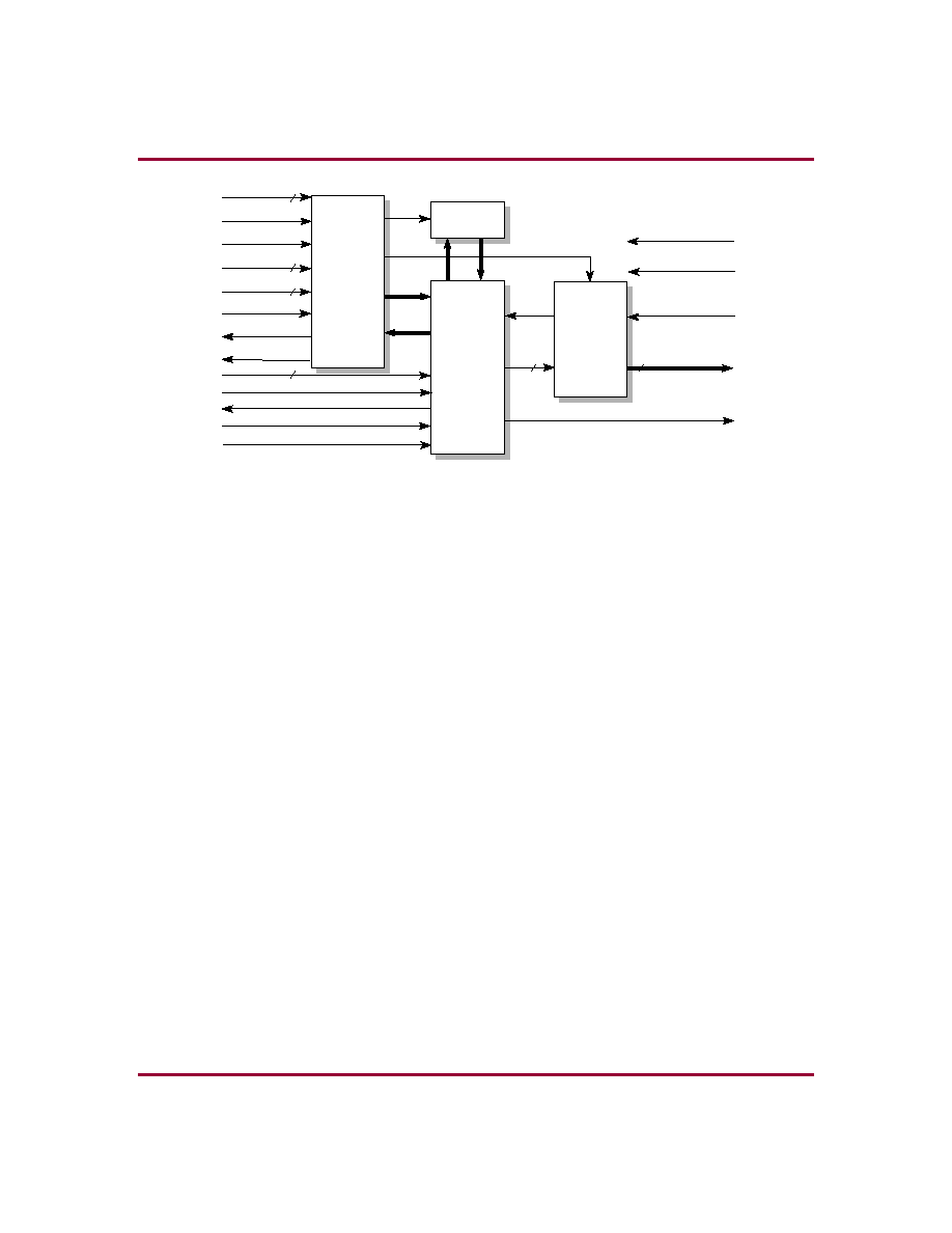
The transmitter is architecturally divided into blocks as
described below and as shown in Figure 2.
Configuration Interface
This block provides programmable registers that control the
functionality of the CC318f transmitter. It includes a set of
eight 8-bit write registers and eleven 8-bit read registers.
The write registers include:
∑
Address field register
∑
Control field register
∑
Protocol field (8/16-bits) registers
∑
Maximum packet length count registers
∑
Configuration register
∑
Interrupt mask register
SONET TxFPGA
Tx Line Drv.
PCI Adaptor
PLX9080
Config EPLD
Tx FIFO
Rx FIFO
Memory
Interface Cntler
Tx PP FPGA
Rx PP FPGA
PPP8 CoreCell Tx
Packets Over SONET
PPP8 CoreCell Rx
SONET RxFPGA
Rx Line Drv.
FPGA Config
Signals
PCI Bus
Local Bus
32
32
32
32
32
32
X8816
Figure 1:
February 14, 2000
3-3
The read registers include:
∑
Status register
∑
Packet sent count registers (TxPktSentCount)
∑
Excess packet sent count registers
(TxExSizePktSentCount)
∑
Transmission break count registers (TransBreakCount)
The configuration of the CC318f Transmitter takes place
only when SoftReset is active. This block also generates an
interrupt whenever the read counters overflow. The various
interrupt sources can be individually masked through the
Interrupt Mask register.
Encapsulator
This block forms the PPP HDLC-like frame described in
RFC1619. The configuration register in the configuration
block programs the encapsulator for various modes of
operation. The encapsulator drops the Address and Control
fields when the CompressEnb bit in the configuration regis-
ter is high. Similarly, only the higher octet (MS byte) from
the protocol field is inserted in the frame when the protocol
field is of 16-bits (TxPrtcl16 bit is high) and PrtclCompres-
sEnb bit is high.
FCS Generator
This block calculates a 16- or 32-bit CRC on the entire
frame between two flag sequences. The encapsulator then
inserts this FCS at the end of each frame. The PktBound-
ary signal indicates the last octet of data. The FCS calcu-
lated is inserted after this octet. The TxFCS32 bit in the
configuration register selects 16 or 32-bit FCS field inser-
tion.
Scrambler
The output of the encapsulator block is given to the scram-
bler. The scrambler, when enabled, scrambles the PHY
interface data. The generating polynomial of this scrambler
is x**43 + 1. When high, the ScrambleEnb bit in the config-
uration register enables the scrambler.
Receiver
The receiver module is architecturally divided into blocks as
described below and as shown in Figure 3.
Configuration and Statistics Interface
This module provides programmable Address, Control and
Protocol fields and MTU (maximum transfer unit). It pro-
vides statistics for number of packets received, valid pack-
ets received, runt packets received, excess size packets
received and frames with address, control, protocol field
error, escape sequence error and FCS error.
The receiver is configured through Write Registers. Statis-
tics are obtained by reading Read Counters. The counters
and registers are accessed through UpAddrIn, UpWriteEnb
and UpReadEnb signals. It has separate input and output
byte-wide data buses.
An interrupt is raised once any statistics counter overflows.
The counter overflow information is maintained in the Sta-
tus Register. Once the Status Register is read it is cleared.
The Interrupt Mask Register masks interrupts on the
respective counters, accomplished by setting an individual
bit in the Interrupt Mask register.
Figure 2: CC318f Transmitter Block Diagram
X9098
TxUpAddrIn
TxUpReadEnb
TxUpWriteEnb
TxUpDataIn
TxUpDataOut
SoftReset
TxReady
TxINTR
TxDataValid
DataReq
PktBoundary
TxClk
Reset
TxDataOutEnb
TxDataOut[7:0]
PktLengthCntOverFlow
Configuration
Interface
FCS Generator
Encapsulator
Scrambler
8
TxDataIn
8
8
4
8
8
TxAbortPacket

PPP8 HDLC Core (CC318f)
3-4
February 14, 2000
De-Encapsulator and Error Generator
This module de-encapsulates frames and analyzes the
address, control and protocol fields. It generates an error
signal for frames received with Address, Control field and
Protocol field errors on respective lines. It silently discards
the frames with address, control or protocol field errors by
disabling the data valid signal for further blocks. It gener-
ates a packet boundary signal when the first FCS byte is
detected by the state machine. It generates a StartOfMes-
sage signal to the interface with the Output Controller.
FCS Verifier
This module verifies the 16- or 32-bit FCS, depending on
the configuration. It generates error on an incorrect FCS. It
accepts byte data with validation for verifying FCS.
Statistics Generator
This module generates an enable signal for Packets
received, Valid packets received, Runt packets and packets
with number of octets greater than MTU (which is program-
mable). It generates a ByteCntOverFlow signal on a 16-bit
byte counter overflow. The signal indicates when a packet
is received with more than 64K bytes.
Output Controller
This module gives out byte data on RxDataOut bus with
validation signal on packet interface It gives out the packet
boundary signal synchronous with the last byte of the
packet. It gives RxDiscardPacket signal to validate the
packet sent on packet interface. The RxDiscardPkt signal is
valid only when RxPktbndry signal is active. A frame with
an FCS error or Invalid frame is indicated on the RxDis-
cardPkt signal.
DeScrambler and Input Controller (PHY
Interface)
This module receives data on the RxDataIn bus with RxClk.
The data is validated by the RxDataValid signal. It removes
the control escape octet from the data path and XORs the
next data byte. It detects Transparency octet errors and the
frames which end with a control escape octet followed
immediately by closing flag sequence. The processed data
is searched for FCS bytes which are stuffed with an addi-
tional bit for identification. It feeds data to other blocks with
a validation signal along with identification bits for flag
sequence and FCS bytes.
The input from the PHY device is first given to the descram-
bler. The descrambler, when enabled, descrambles the
PHY interface data. The polynomial of this descrambler is
x**43 + 1. The descrambler is enabled when the DeScram-
bleEnb bit in the configuration register is high.
Pinout
The pinout is not fixed to any specific device I/O. IOB
counts shown in the AllianceCORE Facts table assume all
core I/O are routed off-chip. Most applications will consume
many of these signals internal to the chip for a complete
design.Signal names for the transmit and receive blocks
are provided in the block diagrams shown in Figures 2 and
3, and described in Tables 2 and 3, respectively.
X8809
RxUpDataOut
RxUpReadEnb
RxUpWriteEnb
RxUpAddrIn
RxUpDataIn
SoftReset
RxReady
RxINTR
RxDataOutValid
RxDataValid
PktBoundary
RxClk
Reset
RxDataIn
RxDataOut
RxDiscardPkt
ByteCntOverFlow
De-Encapsulator
and Error
Generator
8
8
5
Output
Controller
DeScrambler
and Input
Controller
Configuration
Interface
Stastics
Generator
8
8
FCS Verifier
Figure 3: CC318f Receiver Block Diagram

February 14, 2000
3-5
Verification Methods
FPGA verification was done by back annotating the routed
design and simulating in a Model Tech environment. Simu-
lation was performed using a behavioral test bench and
simprim libraries. The RTL code was tested by performing
functional simulation using behavioral test bench, also in
the Model Tech environment.
Recommended Design
Experience
The following experience is recommended for a user to
implement a complete design with the CC318f:
∑
Complete understanding of the RFC1619 specification
document;
∑
Familiarity with the Xilinx FPGA architecture;
∑
Familiarity with the simulation, synthesis, and Xilinx
tools.
∑
Knowledge of ATM and B-ISDN (Broadband ISDN) is
an added advantage.
Table 2: Transmitter Core Signal Pinout
Signal
Signal
Direction
Description
Microprocessor Interface Signals
TxUpAddrIn [3:0]
Input
Address of internal read/write registers.
TxUpReadEnb
Input
Read enable for read registers; Active High.
TxUpWriteEnb
Input
Write enable for write registers; Active High.
TxUpDataIn [7:0]
Input
Write registers data bus.
TxUpDataOut [7:0]
Input
Read registers data bus.
SoftReset
Input
Synchronous reset; Active High.
TxReady
Input
Validates data on TxRegDataOut bus when High.
TxINTR
Input
Level interrupt; Active High.
PktLengthCntOverFlow
Input
Indicates PktLength Counter exceeding specific PktLength value, when High.
Packet Interface Signals
TxDataIn [7:0]
Input
8- bit data input.
TxDataValid
Input
Validates data on TxDataIn bus.
DataReq
Output
When High, requests packet interface to place next data octet on TxDataIn
bus.
PktBoundary
Output
When sampled High, data received on TxData line is considered as last octet
of packet.
TxAbortPacket
Input
When sampled High with PktBoundary signal the present packet is aborted.
PHY Interface Signals
TxDataOutEnb
Output
When sampled High,Transmitter outputs data on TxDataOut bus only.
TxDataOut [7:0]
Output
8-bit output data bus.
Miscellaneous Signals
TxClk
Output
Clock input to Transmitter (uses 1 global buffer IOB).
Reset
Output
Asynchronous reset; Active High.

PPP8 HDLC Core (CC318f)
3-6
February 14, 2000
Available Support Products
CoreEl MicroSystems offers a complete line of support
tools to help customers integrate this core into their Xilinx
design. All of these are available for additional cost from
CoreEl. Contact CoreEl for more information.
PPP8 Test Bench
The PPP8 Test Bench is a group of two independent test
benches for the receiver and transmitter. It is a script-based
test bench.
Evaluation Board
The POS Evaluation Board is a PCI bus based add on card
which accepts/receives IP packets and interfaces to OC-3C
lines. The card transfers IP packets stored in host local
memory over the SONET interface and stores the packets
received over the SONET interface in host local memory.
The transmission and reception of packets is done with
minimum CPU intervention by performing DMA transfers
over the PCI bus.
Ordering Information
For information on this or other products mentioned in this
datasheet, contact CoreEl MicroSystems directly. Contact
information is provided on the front page of this datasheet.
Table 3: Receiver Core Signal Pinout
Signal
Signal
Direction
Description
Microprocessor Interface Signals
ByteCntOverFlow
Output
A pulse indicates overflow of 16-bit frame byte counter. It indicates that frame
length is greater than 64K.
RxUpDatOut[7:0]
Input
Output Data bus for reading contents of receiver registers.
RxUpWriteEnb
Input
Enable signal for writing in addressed register. Requires a one clock-wide read
pulse to initiate one write cycle.
RxUpReadEnb
Input
Enable signal for reading addressed register. Requires a one clock-wide read
pulse to initiate one read cycle.
RxUpAddrIn[4:0]
Input
5-bit Address bus for accessing receiver read and write registers.
RxUpDataIn[7:0]
Input
Input Data bus for configuring receiver
SoftReset
Input
Hardwired synchronous reset; Active High.
RxReady
Output
Validates Data on UpDataOut bus.
RxINTR
Output
Interrupt signal. Enabled on any statistics counter overflow; remains Active un-
til acknowledged.
Packet Interface Signals
RxDataOutValid
Output
Validates data on RxDataOut bus.
RxPktBndry
Output
A pulse indicates last octet of packet data. It is given synchronous with last
byte of packet.
RxDataOut [7:0]
Output
Output Data bus on packet interface.
RxDiscardPkt
Output
Validates packet sent on packet interface. It is to be sampled with RxPktBndry
signal.
PHY Interface Signals
RxDataIn [7:0]
Input
8-bit input data bus on PHY interface.
RxDataValid
Input
Validates data on RxDataIn bus.
Miscellaneous Signals
RxClk
Input
Clock input for Receiver (uses 1 global buffer IOB).
Reset
Input
Active High asynchronous reset.

February 14, 2000
3-7
Related Information
RFC1619 PPP Over SONET Specification Document.
Xilinx Programmable Logic
For information on Xilinx programmable logic or develop-
ment system software, contact your local Xilinx sales office,
or:
Xilinx, Inc.
2100 Logic Drive
San Jose, CA 95124
Phone:
+1 408-559-7778
Fax:
+1 408-559-7114
URL:
www.xilinx.com
For general Xilinx literature, contact:
Phone:
+1 800-231-3386 (inside the US)
+1 408-879-5017 (outside the US)
E-mail:
literature@xilinx.com
For AllianceCORE
TM
specific information, contact:
Phone:
+1 408-879-5381
E-mail:
alliancecore@xilinx.com
URL:
www.xilinx.com/products
/logicore/alliance/tblpart.htm