 | –≠–ª–µ–∫—Ç—Ä–æ–Ω–Ω—ã–π –∫–æ–º–ø–æ–Ω–µ–Ω—Ç: DS023 | –°–∫–∞—á–∞—Ç—å:  PDF PDF  ZIP ZIP |

DS023 (v1.6) June 27, 2002
www.xilinx.com
1
Preliminary Product Specification
1-800-255-7778
© 2002 Xilinx, Inc. All rights reserved. All Xilinx trademarks, registered trademarks, patents, and disclaimers are as listed at
http://www.xilinx.com/legal.htm
.
All other trademarks and registered trademarks are the property of their respective owners. All specifications are subject to change without notice.
Features
∑
Lowest power 32 macrocell CPLD
∑
5.0 ns pin-to-pin logic delays
∑
System frequencies up to 200 MHz
∑
32 macrocells with 750 usable gates
∑
Available in small footprint packages
-
48-ball CS BGA (36 user I/O pins)
-
44-pin VQFP (36 user I/O)
-
44-pin PLCC (36 user I/O)
∑
Optimized for 3.3V systems
-
Ultra-low power operation
-
5V tolerant I/O pins with 3.3V core supply
-
Advanced 0.35 micron five layer metal EEPROM
process
-
Fast Zero PowerTM (FZP) CMOS design
technology
∑
Advanced system features
-
In-system programming
-
Input registers
-
Predictable timing model
-
Up to 23 available clocks per function block
-
Excellent pin retention during design changes
-
Full IEEE Standard 1149.1 boundary-scan (JTAG)
-
Four global clocks
-
Eight product term control terms per function block
∑
Fast ISP programming times
∑
Port Enable pin for dual function of JTAG ISP pins
∑
2.7V to 3.6V supply voltage at industrial temperature
range
∑
Programmable slew rate control per macrocell
∑
Security bit prevents unauthorized access
∑
Refer to XPLA3 family data sheet (
DS012
) for
architecture description
Description
The XCR3032XL is a 3.3V, 32-macrocell CPLD targeted at
power sensitive designs that require leading edge program-
mable logic solutions. A total of two function blocks provide
750 usable gates. Pin-to-pin propagation delays are 5.0 ns
with a maximum system frequency of 200 MHz.
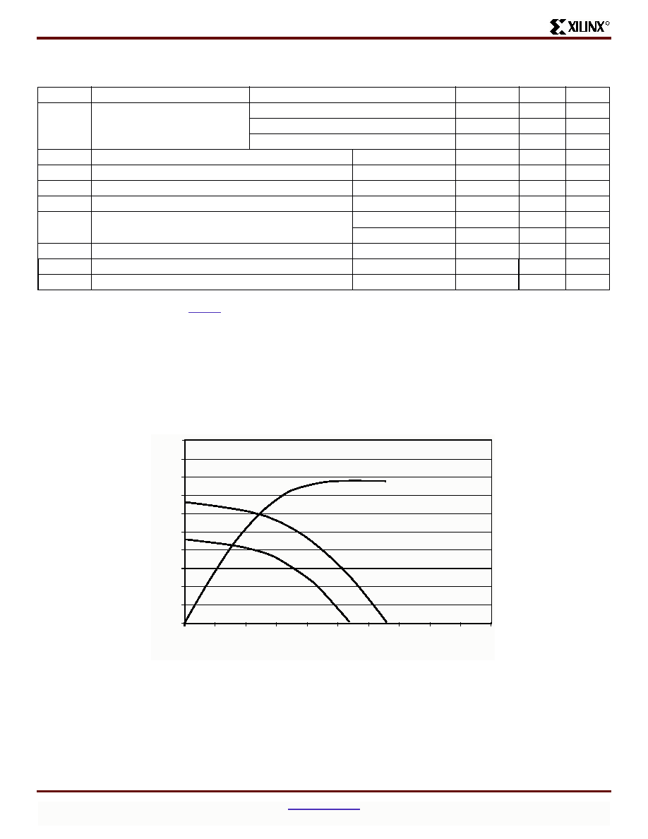
TotalCMOS Design Technique for Fast
Zero Power
Xilinx offers a TotalCMOS CPLD, both in process technol-
ogy and design technique. Xilinx employs a cascade of
CMOS gates to implement its sum of products instead of
the traditional sense amp approach. This CMOS gate imple-
mentation allows Xilinx to offer CPLDs that are both high
performance and low power, breaking the paradigm that to
have low power, you must have low performance. Refer to
Figure 1
and
Table 1
showing the I
CC
vs. Frequency of our
XCR3032XL TotalCMOS CPLD (data taken with two
resetable up/down, 16-bit counters at 3.3V, 25
∞
C).
0
XCR3032XL 32 Macrocell CPLD
DS023 (v1.6) June 27, 2002
0
14
Preliminary Product Specification
R
Figure 1: I
CC
vs. Frequency at V
CC
= 3.3V, 25∞C
5
0
10
15
20
0
20
40
60
80
100
120
140
160
180
200
Frequency (MHz)
DS023_01_080101
Ty
pical I
CC
(
mA
)
Table 1: I
CC
vs. Frequency (V
CC
= 3.3V, 25∞C)
Frequency (MHz)
0
1
5
10
20
50
100
200
Typical I
CC
(mA)
0.02
0.13
0.54
1.06
2.09
5.2
10.26
20.3
XCR3032XL 32 Macrocell CPLD
2
www.xilinx.com
DS023 (v1.6) June 27, 2002
1-800-255-7778
Preliminary Product Specification
R
DC Electrical Characteristics Over Recommended Operating Conditions
(1)
Symbol
Parameter
Test Conditions
Min.
Max.
Unit
V
OH
(
2
)
Output High voltage
V
CC
= 3.0V to 3.6V, I
OH
= ≠8 mA
2.4
-
V
V
CC
= 2.7V to 3.0V, I
OH
= ≠8 mA
2.0
(
3
)
-
V
I
OH
= ≠500
µ
A
90% V
CC
-
V
V
OL
Output Low voltage
I
OL
= 8 mA
-
0.4
V
I
IL
(
4
)
Input leakage current
V
IN
= GND or V
CC
≠10
10
µ
A
I
IH
(
4
)
I/O High-Z leakage current
V
IN
= GND or V
CC
≠10
10
µ
A
I
CCSB
Standby current
V
CC
= 3.6V
-
100
µ
A
I
CC
Dynamic current
(
5
,
6
)
f = 1 MHz
-
0.25
mA
f = 50 MHz
-
7.5
mA
C
IN
Input pin capacitance
(
7
)
f = 1 MHz
-
8
pF
C
CLK
Clock input capacitance
(
7
)
f = 1 MHz
-
12
pF
C
I/O
I/O pin capacitance
(
7
)
f = 1 MHz
-
10
pF
Notes:
1.
See XPLA3 family data sheet (
DS012
) for recommended operating conditions
2.
See
Figure 2
for output drive characteristics of the XPLA3 family.
3.
This parameter guaranteed by design and characterization, not by testing.
4.
Typical leakage current is less than 1
µ
A.
5.
See
Table 1
,
Figure 1
for typical values.
6.
This parameter measured with a 16-bit, resetable up/down counter loaded into every function block, with all outputs disabled and
unloaded. Inputs are tied to V
CC
or ground. This parameter guaranteed by design and characterization, not testing.
7.
Typical values, not tested.
Figure 2: Typical I/V Curve for the XPLA3 Family, 3.3V, 25∞C
0
0
10
20
30
40
50
60
70
80
90
100
0.5
1
1.5
2
2.5
3
3.5
4
4.5
5
Volts
I
OL
(3.3V)
I
OH
(3.3V)
I
OH
(2.7V)
mA
DS012_10_031802
XCR3032XL 32 Macrocell CPLD
DS023 (v1.6) June 27, 2002
www.xilinx.com
3
Preliminary Product Specification
1-800-255-7778
R
AC Electrical Characteristics Over Recommended Operating Conditions
(1,2)
Symbol
Parameter
-5
-7
-10
Unit
Min.
Max.
Min.
Max.
Min.
Max.
T
PD1
Propagation delay time (single p-term)
4.5
-
7.0
-
9.1
ns
T
PD2
Propagation delay time (OR array)
(3)
5.0
-
7.5
-
10.0
ns
T
CO
Clock to output (global synchronous pin clock)
3.5
5.0
-
6.5
ns
T
SUF
Setup time (fast input register)
2.5
-
3.0
-
3.0
-
ns
T
SU1
(4)
Setup time (single p-term)
3.0
-
4.3
-
5.4
-
ns
T
SU2
Setup time (OR array)
3.5
-
4.8
-
6.3
-
ns
T
H
(4)
Hold time
0
-
0
-
0
-
ns
T
WLH
(4)
Global Clock pulse width (High or Low)
2.5
-
3.0
-
4.0
-
ns
T
PLH
(4)
P-term clock pulse width
4.0
-
5.0
-
6.0
-
ns
T
R
(4)
Input rise time
-
20
-
20
-
20
ns
T
L
(4)
Input fall time
-
20
-
20
-
20
ns
f
SYSTEM
(4)
Maximum system frequency
-
200
-
119
-
95
MHz
T
CONFIG
(4)
Configuration time
(5)
-
30
-
30
-
30
µ
s
T
INIT
(4)
ISP initialization time
-
30
-
30
-
30
µ
s
T
POE
(4)
P-term OE to output enabled
-
7.2
-
9.3
-
11.2
ns
T
POD
(4)
P-term OE to output disabled
(6)
-
7.2
-
9.3
-
11.2
ns
T
PCO
(4)
P-term clock to output
-
6.0
-
8.3
-
10.7
ns
T
PAO
(4)
P-term set/reset to output valid
-
6.5
-
9.3
-
11.2
ns
Notes:
1.
Specifications measured with one output switching.
2.
See XPLA3 family data sheet (
DS012
) for recommended operating conditions.
3.
See
Figure 4
for derating.
4.
These parameters guaranteed by design and/or characterization, not testing.
5.
Typical current draw during configuration is 3 mA at 3.6V.
6.
Output C
L
= 5 pF.

XCR3032XL 32 Macrocell CPLD
4
www.xilinx.com
DS023 (v1.6) June 27, 2002
1-800-255-7778
Preliminary Product Specification
R
Internal Timing Parameters
(1,2)
Symbol
Parameter
-5
-7
-10
Unit
Min.
Max.
Min.
Max.
Min.
Max.
Buffer Delays
T
IN
Input buffer delay
-
0.7
-
1.6
-
2.2
ns
T
FIN
Fast Input buffer delay
-
2.2
-
3.0
-
3.1
ns
T
GCK
Global Clock buffer delay
-
0.7
-
1.0
-
1.3
ns
T
OUT
Output buffer delay
-
1.8
-
2.7
-
3.6
ns
T
EN
Output buffer enable/disable delay
-
4.5
-
5.0
-
5.7
ns
Internal Register, Product Term, and Combinatorial Delays
T
LDI
Latch transparent delay
-
1.3
-
1.6
-
2.0
ns
T
SUI
Register setup time
1.0
-
1.0
-
1.2
-
ns
T
HI
Register hold time
0.3
-
0.5
-
0.7
-
ns
T
ECSU
Register clock enable setup time
2.0
-
2.5
-
3.0
-
ns
T
ECHO
Register clock enable hold time
3.0
-
4.5
-
5.5
-
ns
T
COI
Register clock to output delay
-
1.0
-
1.3
-
1.6
ns
T
AOI
Register async. S/R to output delay
-
2.0
-
2.3
-
2.1
ns
T
RAI
Register async. recovery
-
3.5
-
5.0
-
6.0
ns
T
PTCK
Product term clock delay
-
2.5
-
2.7
-
3.3
ns
T
LOGI1
Internal logic delay (single p-term)
-
2.0
-
2.7
-
3.3
ns
T
LOGI2
Internal logic delay (PLA OR term)
-
2.5
-
3.2
-
4.2
ns
Feedback Delays
T
F
ZIA delay
-
0.5
-
2.9
-
3.5
ns
Time Adders
T
LOGI3
Fold-back NAND delay
-
2.0
-
2.5
-
3.0
ns
T
UDA
Universal delay
-
1.2
-
2.0
-
2.5
ns
T
SLEW
Slew rate limited delay
-
4.0
-
5.0
-
6.0
ns
Notes:
1.
These parameters guaranteed by design and characterization, not testing.
2.
See XPLA3 family data sheet (
DS012
) for timing model.

XCR3032XL 32 Macrocell CPLD
DS023 (v1.6) June 27, 2002
www.xilinx.com
5
Preliminary Product Specification
1-800-255-7778
R
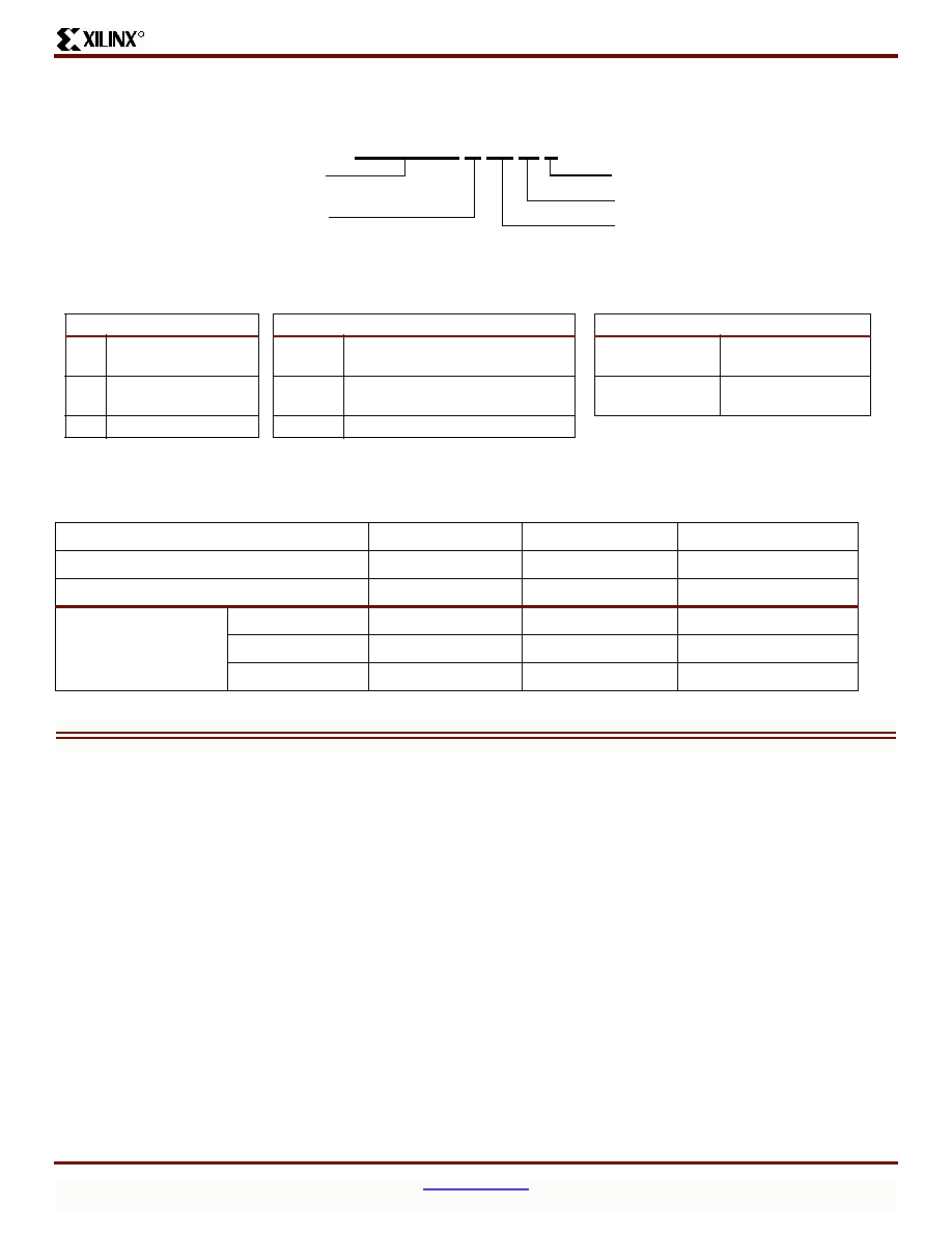
Switching Characteristics
Figure 3: AC Load Circuit
DS023_03_102401
Component
Values
R1
390
R2
390
C1
35 pF
Measurement
S1
S2
T
POE (High)
T
POE (Low)
T
P
Open
Closed
Closed
Open
Closed
Closed
VCC
V
OUT
V
IN
C1
R1
R2
S1
S2
Note: For T
POD
, C1 = 5 pF. Delay measured at
output level of V
OL
+ 300 mV, V
OH
≠ 300 mV.
Figure 4: Derating Curve for T
PD2
3.0
3.5
4.0
4.5
1
2
4
8
16
DS023_05_061101
Outputs
T
PD
(
ns
)
Figure 5: Voltage Waveform
90%
10%
1.5 ns
1.5 ns
DS023_06_042800
+3.0V
0V
Measurements:
All circuit delays are measured at the +1.5V level of
inputs and outputs, unless otherwise specified.
T
R
T
L
XCR3032XL 32 Macrocell CPLD
6
www.xilinx.com
DS023 (v1.6) June 27, 2002
1-800-255-7778
Preliminary Product Specification
R
Pin Descriptions
Table 2: XCR3032XL User I/O Pins
PC44
VQ44
CS48
Total User I/O Pins
36
36
36
Table 3: XCR3032XL I/O Pins
Function
Block
Macrocell
PC44
VQ44
CS48
1
1
4
42
A2
1
2
5
43
A1
1
3
6
44
C4
1
4
7
(1)
1
(1)
B1
(1)
1
5
8
2
C2
1
6
9
3
C1
1
7
11
5
D3
1
8
12
6
D1
1
9
13
(1)
7
(1)
D2
(1)
1
10
14
8
E1
1
11
16
10
F1
1
12
17
11
G1
1
13
18
12
E4
1
14
19
13
F2
1
15
20
14
G2
1
16
21
15
F3
2
1
41
35
C5
2
2
40
34
A6
2
3
39
33
B6
2
4
38
(1)
32
(1)
B7
(1)
2
5
37
31
D4
2
6
36
30
C6
2
7
34
28
D6
2
8
33
27
D7
2
9
32
(1)
26
(1)
E5
(1)
2
10
31
25
E7
2
11
29
23
F7
2
12
28
22
G7
2
13
27
21
G6
2
14
26
20
F5
2
15
25
19
G5
2
16
24
18
F4
Notes:
1.
JTAG pins
Table 4: XCR3032XL Global, JTAG, Port Enable, Power,
and No Connect Pins
Pin Type
PC44
VQ44
CS48
IN0 / CLK0
2
40
A3
IN1 / CLK1
1
39
B4
IN2 / CLK2
44
38
A4
IN3 / CLK3
43
37
B5
TCK
32
26
E5
TDI
7
1
B1
TDO
38
32
B7
TMS
13
7
D2
PORT_EN
10
(1)
4
(1)
C3
(1)
V
CC
3, 15, 23,
35
9, 17, 29,
41
B3, C7,
E2, G4
GND
22, 30, 42
16, 24, 36
A5, E3, E6
No Connects
-
-
A7, B2,
F6, G3
Notes:
1.
Port Enable is brought High to enable JTAG pins when
JTAG pins are used as I/O. See family data sheet
(
DS012)
for full explanation.
Table 3: XCR3032XL I/O Pins
Function
Block
Macrocell
PC44
VQ44
CS48
XCR3032XL 32 Macrocell CPLD
DS023 (v1.6) June 27, 2002
www.xilinx.com
7
Preliminary Product Specification
1-800-255-7778
R
Ordering Information
Component Availability
Pins
44
44
48
Type
Plastic PLCC
Plastic VQFP
Plastic BGA
Code
PC44
VQ44
CS48
XCR3032XL
-5
C
C
C
-7
C,I
C,I
C,I
-10
C, I
C, I
C, I
XCR3032XL -5 VQ 44 C
Example:
Temperature Range
Number of Pins
Package Type
Device Type
Speed Grade
Device Ordering Options
Speed
Package
Temperature
-10
10 ns pin-to-pin
delay
PC44
44-pin Plastic Lead Chip Carrier
(PLCC)
C = Commercial
T
A
= 0∞C to +70∞C
V
CC
= 3.0V to 3.6V
-7
7.5 ns pin-to-pin
delay
VQ44
44-pin Very Thin Quad Flat Pack
(VQFP)
I = Industrial
T
A
= ≠40∞C to +85∞C
V
CC
= 2.7V to 3.6V
-5
5 ns pin-to-pin delay
CS48
48-ball Chip Scale Package

XCR3032XL 32 Macrocell CPLD
8
www.xilinx.com
DS023 (v1.6) June 27, 2002
1-800-255-7778
Preliminary Product Specification
R
Revision History
The following table shows the revision history for this document.
Date
Version
Revision
11/18/00
1.0
Initial Xilinx release.
02/05/01
1.1
Removed Timing Model.
04/11/01
1.2
Update TSUF spec to meet UMC characterization data. Added Icc vs. Freq. numbers,
Table 1
and updated
Figure 1
. Added Typical I/V curve,
Figure 2
; added
Table 2
: Total User
I/O; changed V
OH
spec.
04/19/01
1.3
Updated Typical I/V curve,
Figure 2
: added voltage levels.
08/27/01
1.4
Changed from Advance to Preliminary; updated DC Electrical Characteristics; AC Electrical
Characteristics; Internal Timing Parameters; added Derating Curve; added -10 industrial
packages. Added 200 MHz to
Figure 1
and
Table 1
. changed -5 F
SYSTEM
to 200 MHz, -5 T
F
to 0.5 ns.
01/08/02
1.5
Updated T
HI
spec to correct a typo. Added single p-term setup time (T
SU1
) to AC Table,
renamed T
SU
to T
SU2
for setup time through the OR array. Updated AC Load Circuit diagram
to more closely resemble true test conditions, added note for T
POD
delay
measurement.Updated note 5 in AC Characteristics table lowering typical current draw
during configuration.
06/27/02
1.6
Added voltage and temperature to
Figure 2
. Increased -5 T
PCO
to 6.0 (from 5.5 ns) by
adding T
PTCK
parameter to internal timing model.