
DS070 (v2.1) June 1, 2000
www.xilinx.com
1
Product Specification
1-800-255-7778
© 2000 Xilinx, Inc. All rights reserved. All Xilinx trademarks, registered trademarks, patents, and disclaimers are as listed at
http://www.xilinx.com/legal.htm
.
All other trademarks and registered trademarks are the property of their respective owners. All specifications are subject to change without notice.
Features
∑
Certified to MIL-PRF-38535 Appendix A QML
(Qualified Manufacturer Listing.)
∑
Also available under the following Standard Microcircuit
Drawings (SMD): 5962-94717 and 5962-95617.
∑
Configuration one-time programmable (OTP) read-only
memory designed to store configuration bitstreams of
Xilinx FPGA devices
∑
On-chip address counter, incremented by each rising
edge on the clock input
∑
Simple interface to the FPGA requires only one user
I/O pin
∑
Cascadable for storing longer or multiple bitstreams
∑
Programmable reset polarity (active High or active
Low) for compatibility with different FPGA solutions
∑
Low-power CMOS EPROM process
∑
Available in 5V version only
∑
Programming support by leading programmer
manufacturers.
∑
Design support using the Xilinx Alliance and
Foundation series software packages.
Description
The XC1700D QPROTM family of configuration PROMs pro-
vide an easy-to-use, cost-effective method for storing Xilinx
FPGA configuration bitstreams.
When the FPGA is in Master Serial mode, it generates a
configuration clock that drives the PROM. A short access
time after the rising clock edge, data appears on the PROM
DATA output pin that is connected to the FPGA D
IN
pin. The
FPGA generates the appropriate number of clock pulses to
complete the configuration. Once configured, it disables the
PROM. When the FPGA is in Slave Serial mode, the PROM
and the FPGA must both be clocked by an incoming signal.
Multiple devices can be concatenated by using the CEO
output to drive the CE input of the following device. The
clock inputs and the DATA outputs of all PROMs in this
chain are interconnected. All devices are compatible and
can be cascaded with other members of the family.
For device programming, either the Xilinx AllianceTM or the
FoundationTM series development systems compiles the
FPGA design file into a standard HEX format which is then
transferred to most commercial PROM programmers.
0
QPRO Family of XC1700D QML
Configuration PROMs
DS070 (v2.1) June 1, 2000
0
2
Product Specification
R
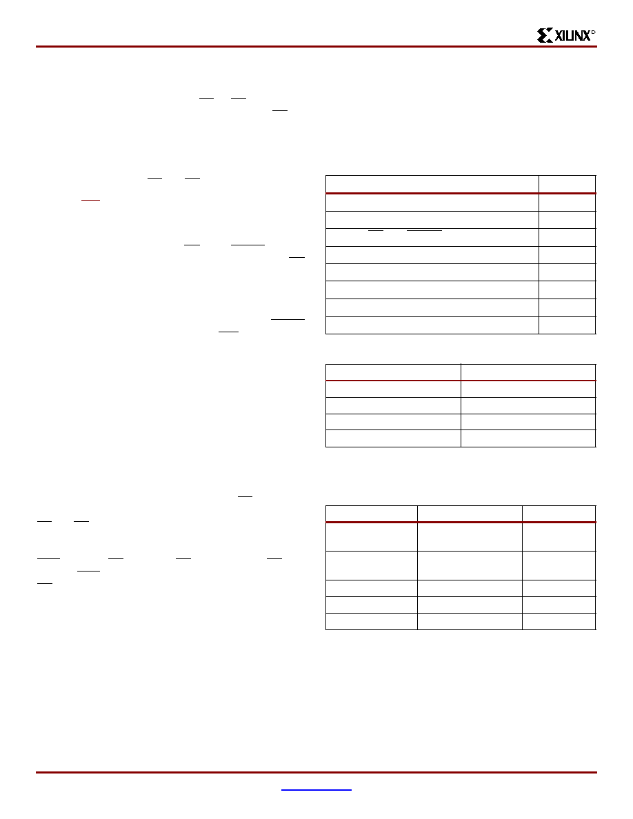
Figure 1: Simplified Block Diagram (does not show programming circuit)
EPROM
Cell
Matrix
Address Counter
CE
DATA
OE
Output
CLK
VCC
VPP
GND
DS027_01_021500
TC
OE
RESET/
OE/
RESET
or
CEO
QPRO Family of XC1700D QML Configuration PROMs
2
www.xilinx.com
DS070 (v2.1) June 1, 2000
1-800-255-7778
Product Specification
R
Pin Description
DATA
Data output, 3-stated when either CE or OE are inactive.
During programming, the DATA pin is I/O. Note that OE can
be programmed to be either active High or active Low.
CLK
Each rising edge on the CLK input increments the internal
address counter, if both CE and OE are active.
RESET/OE
When High, this input holds the address counter reset and
3-states the DATA output. The polarity of this input pin is
programmable as either RESET/OE or OE/RESET. To avoid
confusion, this document describes the pin as RESET/OE,
although the opposite polarity is possible on all devices.
When RESET is active, the address counter is held at zero,
and the DATA output is put in a high-impedance state. The
polarity of this input is programmable. The default is active
High RESET, but the preferred option is active Low RESET,
because it can be driven by the FPGAs INIT pin.
The polarity of this pin is controlled in the programmer inter-
face. This input pin is easily inverted using the Xilinx
HW-130 programmer software. Third-party programmers
have different methods to invert this pin.
CE
When High, this pin disables the internal address counter,
3-states the DATA output, and forces the device into low-I
CC
standby mode.
CEO
Chip Enable output, to be connected to the CE input of the
next PROM in the daisy chain. This output is Low when the
CE and OE inputs are both active AND the internal address
counter has been incremented beyond its Terminal Count
(TC) value. In other words: when the PROM has been read,
CEO will follow CE as long as OE is active. When OE goes
inactive, CEO stays High until the PROM is reset. Note that
OE can be programmed to be either active High or active
Low.
V
PP
Programming voltage. No overshoot above the specified
max voltage is permitted on this pin. For normal read oper-
ation, this pin must be connected to V
CC
. Failure to do so
may lead to unpredictable, temperature-dependent opera-
tion and severe problems in circuit debugging. Do not leave
V
PP
floating!
V
CC
and GND
V
CC
is positive supply pin and GND is ground pin.
PROM Pinouts
Capacity
Number of Configuration Bits, Including
Header for Xilinx FPGAs and Compatible
PROMs
Pin Name
8-pin
DATA
1
CLK
2
RESET/OE (OE/RESET)
3
CE
4
GND
5
CEO
6
V
PP
7
V
CC
8
Device
Configuration Bits
XC1736D
36,288
XC1765D
65,536
XC17128D
131,072
XC17256D
262,144
Device
Configuration Bits
PROM
XC3000/A series
14,819 to 94,984
XC1765D to
XC17128D
XC4000 series
95,008 to 247,968
XC17128D to
XC17256D
XQ4005E
95,008
XC17128D
XQ4010E
178,144
XC17256D
XQ4013E
247,968
XC17256D

QPRO Family of XC1700D QML Configuration PROMs
DS070 (v2.1) June 1, 2000
www.xilinx.com
3
Product Specification
1-800-255-7778
R
Controlling PROMs
Connecting the FPGA device with the PROM.
∑
The DATA output(s) of the PROM(s) drives the D
IN
input of the lead FPGA device.
∑
The Master FPGA CCLK output drives the CLK input(s)
of the PROM(s).
∑
The CEO output of a PROM drives the CE input of the
next PROM in a daisy chain (if any).
∑
The RESET/OE input of all PROMs is best driven by
the INIT output of the lead FPGA device. This
connection assures that the PROM address counter is
reset before the start of any (re)configuration, even
when a reconfiguration is initiated by a V
CC
glitch.
Other methods--such as driving RESET/OE from LDC
or system reset--assume the PROM internal
power-on-reset is always in step with the FPGA's
internal power-on-reset. This may not be a safe
assumption.
∑
The PROM CE input can be driven from either the LDC
or DONE pins. Using LDC avoids potential contention
on the D
IN
pin.
∑
The CE input of the lead (or only) PROM is driven by
the DONE output of the lead FPGA device, provided
that DONE is not permanently grounded. Otherwise,
LDC can be used to drive CE, but must then be
unconditionally High during user operation. CE can
also be permanently tied Low, but this keeps the DATA
output active and causes an unnecessary supply
current of 10 mA maximum.
FPGA Master Serial Mode Summary
The I/O and logic functions of the Configurable Logic Block
(CLB) and their associated interconnections are established
by a configuration program. The program is loaded either
automatically upon power up, or on command, depending
on the state of the three FPGA mode pins. In Master Serial
mode, the FPGA automatically loads the configuration pro-
gram from an external memory. The Xilinx PROMs have
been designed for compatibility with the Master Serial
mode.
Upon power-up or reconfiguration, an FPGA enters the
Master Serial mode whenever all three of the FPGA
mode-select pins are Low (M0=0, M1=0, M2=0). Data is
read from the PROM sequentially on a single data line. Syn-
chronization is provided by the rising edge of the temporary
signal CCLK, which is generated during configuration.
Master Serial Mode provides a simple configuration inter-
face. Only a serial data line and two control lines are
required to configure an FPGA. Data from the PROM is
read sequentially, accessed via the internal address and bit
counters which are incremented on every valid rising edge
of CCLK.
If the user-programmable, dual-function D
IN
pin on the
FPGA is used only for configuration, it must still be held at a
defined level during normal operation. Xilinx FPGAs take
care of this automatically with an on-chip default pull-up
resistor.
Programming the FPGA With Counters
Unchanged Upon Completion
When multiple FPGA-configurations for a single FPGA are
stored in a PROM, the OE pin should be tied Low. Upon
power-up, the internal address counters are reset and con-
figuration begins with the first program stored in memory.
Since the OE pin is held Low, the address counters are left
unchanged after configuration is complete. Therefore, to
reprogram the FPGA with another program, the DONE line
is pulled Low and configuration begins at the last value of
the address counters.
This method fails if a user applies RESET during the FPGA
configuration process. The FPGA aborts the configuration
and then restarts a new configuration, as intended, but the
PROM does not reset its address counter, since it never
saw a High level on its OE input. The new configuration,
therefore, reads the remaining data in the PROM and inter-
prets it as preamble, length count etc. Since the FPGA is
the master, it issues the necessary number of CCLK pulses,
up to 16 million (2
24
) and DONE goes High. However, the
FPGA configuration will be completely wrong, with potential
contentions inside the FPGA and on its output pins. This
method must, therefore, never be used when there is any
chance of external reset during configuration.
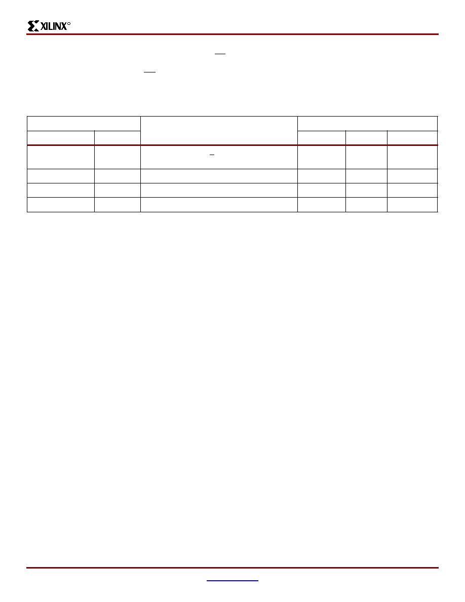
Cascading Configuration PROMs
For multiple FPGAs configured as a daisy-chain, or for
future FPGAs requiring larger configuration memories, cas-
caded PROMs provide additional memory. After the last bit
from the first PROM is read, the next clock signal to the
PROM asserts its CEO output Low and disables its DATA
line. The second PROM recognizes the Low level on its CE
input and enables its DATA output. See
Figure 2
.
After configuration is complete, the address counters of all
cascaded PROMs are reset if the FPGA RESET pin goes
Low, assuming the PROM reset polarity option has been
inverted.
To reprogram the FPGA with another program, the DONE
line goes Low and configuration begins where the address
counters had stopped. In this case, avoid contention
between DATA and the configured I/O use of D
IN
.

QPRO Family of XC1700D QML Configuration PROMs
4
www.xilinx.com
DS070 (v2.1) June 1, 2000
1-800-255-7778
Product Specification
R
Figure 2: Master Serial Mode. The one-time-programmable PROM supports automatic loading of configuration programs.
Multiple devices can be cascaded to support additional FPGAs. An early DONE inhibits the PROM data output one CCLK
cycle before the FPGA I/Os become active.
DIN
DOUT
CCLK
INIT
DONE
PROM
DATA
CLK
CE
CE
FPGA
(Low Resets the Address Pointer)
* For mode pin connections,
refer to the appropriate FPGA data sheet.
Vcc
VCC
VCC
OPTIONAL
Daisy-chained
FPGAs with
Different
configurations
OPTIONAL
Slave FPGAs
with Identical
Configurations
RESET
RESET
DS027_02_052200
CCLK
(Output)
DIN
DOUT
(Output)
OE/RESET
MODES*
VPP
VPP
Cascaded
Serial
Memory
DATA
CLK
CEO
OE/RESET
3.3V
4.7K
QPRO Family of XC1700D QML Configuration PROMs
DS070 (v2.1) June 1, 2000
www.xilinx.com
5
Product Specification
1-800-255-7778
R
Standby Mode
The PROM enters a low-power standby mode whenever CE
is asserted High. The output remains in a high impedance
state regardless of the state of the OE input.
Programming
The devices can be programmed on programmers supplied
by Xilinx or qualified third-party vendors. The user must
ensure that the appropriate programming algorithm and the
latest version of the programmer software are used. The
wrong choice can permanently damage the device.
Important:
Always tie the V
PP
pin to V
CC
in your application. Never leave V
PP
floating.
Table 1: Truth Table for XC1700 Control Inputs
Control Inputs
Internal Address
Outputs
RESET
CE
DATA
CEO
I
CC
Inactive
Low
If address < TC: increment
If address > TC: don't change
Active
High-Z
High
Low
Active
reduced
Active
Low
Held reset
High-Z
High
Active
Inactive
High
Not changing
High-Z
High
Standby
Active
High
Held reset
High-Z
High
Standby
Notes:
1.
The XC1700 RESET input has programmable polarity
2.
TC = Terminal Count = highest address value. TC + 1 = address 0.