
XILINX PROGRAMMER QUALIFICATION SPECIFICATION
XC17S00 & XC17S00XL Family
03/00 Rev. 2.1
1
nc
nc
1
nc
nc
7
8
CEO
nc
nc
2
3
4
5
6
CE
nc
nc
9
10
11
12
13
14
15
16
17
18
19
20
DATA
CLK
RESET/OE
nc
nc
Vcc
Vpp
nc
nc
GND
2
3
7
6
1
8
4
5
DATA
CLK
RESET/OE
CE
GND
CEO
Vpp
Vcc
Description
The Spartan Family of Serial Configuration
PROMs provide easy-to-use, cost-effective
configuration memory for Xilinx Field
Programmable Gate Arrays.
These devices use a simple serial-access procedure
to configure one or more LCA devices. The user
can select the polarity of the reset function by
programming a special bit. These devices are fully
compatible and can be cascaded with other
members of the XC17S00 family of devices.
8 Pin Dip/VOIC Assignments
All devices are available in the 8 pin DIP and 8
pin VOIC package except the XC17S40,
XC17S40XL, XC17S50XL, XC17S100XL, and
XC17S150XL which comes in the 8 pin DIP
and 20 pin SOIC package (See below).
20-Pin SOIC Assignment (17S40/XL, 50XL,
100XL, 150XL Only)
The Spartan Family consists of 5 volt and
3.3 volt devices. For each 5 volt device
(XC17S00), there is a 3.3 volt counterpart
(XC17S00XL). All devices are one-time
programmable (OTP) and are organized as
follows:
XC17S05
65,536
x 1 bit
XC17S05XL
131,072
x 1 bit
XC17S10/XL
131,072
x 1 bit
XC17S20/XL
262,144
x 1 bit
XC17S30/XL
262,144
x 1 bit
XC17S40/XL
524,288
x 1 bit
XC17S50XL
1, 048,576
x 1 bit
XC17S100XL
1, 048,576
x 1 bit
XC17S150XL
1, 048,576
x 1 bit

XILINX PROGRAMMER QUALIFICATION SPECIFICATION
XC17S00 & XC17S00XL Family
03/00 Rev. 2.1
2
Programming Overview
All the Spartan SPROMs are internally
organized in rows, each row containing eight
(8) words. The S05 device has 32 bit words
and the S05XL, S10/XL, S20/XL, S30/XL and
S40/XL has 64 bit words. Additional non-data
rows are used to read the
Manufacturer's/Device ID and set the Reset
Polarity and cannot be used to store
configuration data. The device programmer
should prompt the user for the desired Reset
Polarity.
Figure 1 shows the flow of how the SPROMs
are programmed. See Figure 2 for the
programming cycle overview and Figure 4 for
the details of the programming cycle.
Enter Programming Mode
The programming mode is entered by holding
and
High with V
PP
at
V
PP1
for two rising
clock
edges, then lowering
V
PP
to
V
PPNOM
for
one more rising clock edge
(See Figure 3).
Once in the programming mode, the following
functions are available.
Read Manufacturer's/Device ID
All of the SPROMs contain a Manufacturer's
and Device identification code. Prior to
attempting to program or verify the device, the
device programmer should read this code and
verify that it is the correct code for the device
selected by the user. If not, display message
"Manufacturer or Device ID Error."
To read the Manufacturer's/Device
identification code, first enter the programming
mode. While holding
High and
Low,
apply N
IDCLK
(See Table 1) clock signals to the
clock pin to access the ID row.
Table I Clock To ID (decimal)
N
IDCLK
N
RSTCLK
S05
2,056
2,048
S05XL
4,600
4,104
S10/XL
4,600
4,104
S20/XL
4,600
4,104
S30/XL
4,600
4,104
S40/XL
19,791
16,384
S50XL
19,791
16,384
S100XL
19,791
16,384
S150XL
19,791
16,384
Then bring
High and
Low* . The first bit
of the identification word is present when
goes Low and does not require a clock. Apply
15 additional clock signals to the CLK pin to
read the complete device ID.
The Manufacturer's/Device ID
Consisting of 2 bytes of data. The first byte
contains the JEDEC assigned Manufacturer's
ID code for Xilinx (C9). The first four bits of the
second byte define the density of the PROM
(See Table ll), while the last four bits of the
second byte contain specific programming
algorithm code (See Table lll). The data is read
out MSB first.
Table ll Density Codes
Device
Density Codes
S05
F (1111)
S10/S10XL/S05XL
8 (1000)
S20/S20XL/S30/S30XL
A (1010)
S40/S40XL
9 (1001)
S50XL
9 (1101)
S100XL
9 (1101)
S150XL
9 (1101)

XILINX PROGRAMMER QUALIFICATION SPECIFICATION
XC17S00 & XC17S00XL Family
03/00 Rev. 2.1
3
Table lll Programming Algo Codes
Device
Algorithm Code
S10XL/S20XL/S40XL
9 (1001)
S05/S10/S20/S40
8 (1000)
S30XL/S05XL
7 (0111)
S30
6 (0110)
S50XL
6 (0110)
S100XL
7 (0111)
S150XL
9 (1001)
Loading and Programming a Data Word
The data word is shifted into the SPROM, one bit
at a time, on the rising edge of the clock, while
and
are High. The data word counter is
temporarily held in internal latches until the
address is advanced to the next address, and is
programmed into the memory as an entire word
upon strobing the device with V
PP
at V
PP1
for
100
�
s.
The contents of the data word must now be
verified at V
PP2
. The data word is read while
lowering
and capturing the data while clocking
the device 31 or 63 times (See Programming
Overview). The first bit of the word (LSB) is
present when
goes low. After all bits were
read, bring
high and compare the data to the
original file data. If the data does not compare,
stroke V
PP
at V
PP1
for 500
�
s. (Note, the original
data is still contained in internal latches and does
not have to be loaded into the device again.)
Read the data word again (as described above)
and compare it to the original data. If it still does
not compare, pulse V
PP
at V
PP1
for another 500
�
s.
Now read the data word again. If it still does not
compare, power the device down and issue
message: "Device Failed to Program". See Figure
4. If the word compares, increment the word
counter as described below.
Increment the Address (Word) Counter
After successfully programming a data word, the
address counter must be incremented. This is
done on the rising edge of the clock while
is
High and
is Low.*
Set RESET Polarity
The polarity of the Reset/
pin may be made
active Low by writing zeros into a dedicated
row.(See Figure 5).
Reset/
is located outside of the user data
array. Enter the programming mode, then
lower Reset/
, hold the Data pin Low, strobe
the clock N
RSTCLK
times (See Table l), raise the
Reset/
pin, load the data latches with all
zeros (see Load a Data Word above), and
strobe V
PP
at
V
PP1
for 5 ms.
The reset polarity has to be verified (sensed) at
V
PP2
while in programming mode. To sense the
polarity bit, after strobing V
PP
for 5ms, set
low and sense the
pin. If
is high, reset
is active low (successfully programmed). If
is low, reset is active high (failed to program).
Writing ones or not writing anything maintains
RESET active High.
Note:
The Reset Polarity is actually only the MSB of
the data word.
* Be careful not to have
and
Low at the
same time, as this causes the device to exit
programming mode.

XILINX PROGRAMMER QUALIFICATION SPECIFICATION
XC17S00 & XC17S00XL Family
03/00 Rev. 2.1
4
Sensing RESET Polarity
To sense or read the polarity of the Reset/
pin, enter the programming mode, then lower
Reset/
, hold the Data pin High, then strobe
the clock N
RSTCLK
times (See Table l). Set
Reset/
High, set
Low and sense the
pin. If
is High, Reset is active Low. If
is
Low, Reset is active High. The reset polarity bit
is defaulted (unprogrammed) to active high.
When the reset bit is programmed, the "reset"
polarity is active low.
Exit Programming Mode
To exit the programming mode, remove power
from the device, per Figure 6.
Stand Alone Verify Of Data Bits
(Normal Mode)
The verify operation should be performed after
programming. Power up the device and read
the data bits out serially in normal readout
mode (see Figure 7). A margin voltage
(difference between V
PP
and V
CC
) is applied to
the device to ensure charge retention on each
programmed bit. Set V
CC
to V
CCVFY
and V
PP
to
V
PPVFY
. When in normal mode, the Reset/
signal should be driven active high if the reset
polarity bit was unprogrammed (logic "1"). It
should be driven active low if the reset polarity
bit was programmed (logic "0").
At the end of the verify operation the
programmer must confirm that the
pin has
gone Low one clock after the last bit is read
out.
If the data fails to verify, display message
"Failed Margin Verify". If the data verifies,
display message "Device Passed".

XILINX PROGRAMMER QUALIFICATION SPECIFICATION
XC17S00, & XC17S00XL Family
03/00 Rev. 2.1
5
Programming Mode Pin Assignments
DIP8
Pin
VOIC8
Pin
SOIC20
Pin
Name
I/O
Description
1
1
1
Data
I/O The rising edge of the clock shifts a data word in or out of
the SPROM one bit at a time.
2
2
3
CLK
I
Clock input. Used to increment the internal address/word
counter for reading and programming.
3
3
8
RESET/
I
The rising edge of CLK shifts a data word into the PROM
when
and
are High; it shifts a data word out of the
PROM when
is Low and
is High. The
address/word counter is incremented on the rising edge
of CLK while
is held High and
is held Low. Note:
Any modified polarity of the RESET/
pin is ignored in
the programming mode.
4
4
10
I
The rising edge of CLK shifts a data word into the PROM
when
and
are High; it shifts a data word out of the
PROM when
is Low and
is High. The
address/word counter is incremented on the rising edge
of CLK while
is held High and
is held Low.
5
5
11
GND
Ground pin
6
6
13
O
The polarity of the RESET/
pin can be read by sensing
the
pin. Note: The polarity of the RESET/
pin is
ignored while in the programming mode. In final
verification, this pin must be monitored to go Low one
clock cycle after the last data bit has been read.
7
7
18
V
PP
Programming Voltage Supply. Programming mode is
entered by holding
and
High and V
PP
at V
PP1
for
two rising clock edges and then lowering V
PP
to V
PPNOM
for one more rising clock edge. A word is programmed by
strobing the device with V
PP
for the duration T
PGM
. V
PP
must be held at V
CC
for normal operation.
8
8
20
V
CC
V
CC
power supply input.

XILINX PROGRAMMER QUALIFICATION SPECIFICATION
XC17S00, & XC17S00XL Family
03/00 Rev. 2.1
6
DC Programming Specifications
Symbol
Description
Min
Recommended
Max Units
V
CCP*
Supply voltage during programming
5.0
V
V
IL
Low-level input voltage
0.0
0.0
0.5
V
V
IH
High-level input voltage
2.4
V
CC
V
CC
V
V
OL
Low-level output voltage
0.4
V
V
OH
High-level output voltage
2.5
V
V
PP1**
Programming voltage
12.0
12.25
12.5
V
V
PP2***
Margin verify voltage during programming
5.4
V
I
PPP
Supply current on programming pin
60
mA
V
CCNOM/
V
PPNOM
Nominal Voltage
5.0
V
V
CCVFY (S00 Only)
Supply voltage during stand alone margin
verify (5 volt devices)
5.0
V
V
CCVFY (S00XL Only)
Supply voltage during stand alone margin
verify (3.3 volt devices)
3.3
V
V
PPVFY (S00 Only)
Margin voltage during stand alone margin
verify (5 volt devices)
5.4
V
V
PPVFY (S00XL Only)
Margin voltage during stand alone margin
verify (3.3 volt devices)
3.7
V
* Noise and voltage deviation allowed: 5.0V � 50 mV.
** No overshoot is permitted on signal. V
PP
must not be allowed to exceed
V
PP1
max.
*** Noise and voltage deviation allowed: 5.4V � 250 mV.

XILINX PROGRAMMER QUALIFICATION SPECIFICATION
XC17S00, & XC17S00XL Family
03/00 Rev. 2.1
7
AC Programming Specifications
Symbol
Description
Min
Rec
Max Units
1
T
RPP*
10% to 90% rise time of V
PP
5
�s
2
T
FPP*
90% to 10% fall time V
PP
5
�s
3
T
PGM
V
PP
programming pulse width
90
100 (500 Retry)
�s
4
T
SVC
V
PP
setup to CLK for entering programming
100
ns
5
T
HVC
V
PP
hold from CLK for entering programming
300
ns
6
T
SDP
Data setup to CLK for programming
50
ns
7
T
HDP
Data hold from CLK for programming
0
ns
8
T
SCC
setup from programming/verifying
100
ns
9
T
ON
Reset Pulse Width
5
ms
10
T
SCV
hold from CLK for programming/verifying
100
ns
11
T
HCV
hold from V
PP
for programming
50
ns
12
T
SIC
setup to CLK for incrementing address
100
ns
13
T
HIC
hold from CLK for incrementing address
0
ns
14
T
CAC
CLK to data valid
400
ns
15
T
OH
Data hold from CLK
0
ns
16
T
CE
low to data valid
250
ns
* Use the fastest rise and fall time (permitting no overshoot or undershoot) your hardware can
support.

XILINX PROGRAMMER QUALIFICATION SPECIFICATION
XC17S00, & XC17S00XL Family
03/00 Rev. 2.1
8
Code Message
A
Manufacturer Or Device ID Error
B
Device Not Blank
C
Device Not Blank, Reset Polarity Low
D
Device Failed To Program
E
Reset Failed To Program
F
Failed Margin Verify
G
Device Passed
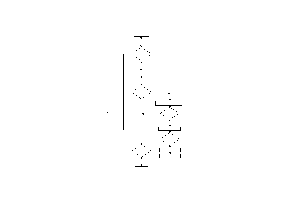
Figure 1. Programming Flow
Read Mfg Code
Read Device ID
Device Data
Array Blank
Reset Active
High
Start
Enter PGM Mode
Issue Error Message "A"
Power Down
Power Up In Read Mode
(Normal Mode)
Power Down
Enter PGM Mode
Sense Reset Polarity State
Power Down
Issue Error Message "A"
Yes
No
Incorrect
Incorrect
Issue Message "B"
No
Yes
Correct
Issue Message "C"
I
Correct
XILINX PROGRAMMER QUALIFICATION SPECIFICATION
XC17S00, & XC17S00XL Family
03/00 Rev. 2.1
9
Data Word Blank
(FFFFFFFFFFFFF
FFFH)
Compare Device
Word To Data
Word
Enter PGM Mode
Increment Address
Counter
Pass
Load Data Word To Device
Pulse V
PP
to V
PP1
for 100us
Read Device Word
Fail
Pass
Yes
No
I
No
Last Data
Word?
Yes
Power Down
II
Compare
Device Word To
Data Word
Fail
Compare
Device Word To
Data Word
Power Down
Fail
Pulse V
PP
to V
PP1
For 500us
Read Device Word
Issue Msg "D"
Pass
Pulse V
PP
to V
PP1
for 500us
Read Device Word
*32 or 64 bits, See Programming Overview
Figure 1. Programming Flow (Continued)

XILINX PROGRAMMER QUALIFICATION SPECIFICATION
XC17S00, & XC17S00XL Family
03/00 Rev. 2.1
10
Program Reset
Polarity
Yes/Pass
Enter Programming Mode
Clock To Reset Row
Load Data Latches With O's
Fail
No
Pulse V
PP
With V
PP1
For 5ms
Sense CEO Reset
Active Low?
No/Fail
II
Yes
Pass
Fail
Margin Verify
All Data Bits
Device Power Off
Exit Programming Mode
Device Power Off
Power Up In Read Mode
V
CC
= V
CCVFY
V
PP
= V
PPVFY
Issue Message "G"
Stop
Device Power Off
Issue Message "E"
Stop
Device Power Off
Issue Message "F"
Figure 1. Programming Flow (Continued)
XILINX PROGRAMMER QUALIFICATION SPECIFICATION
XC17S00, & XC17S00XL
03/00 Rev. 2.1
11
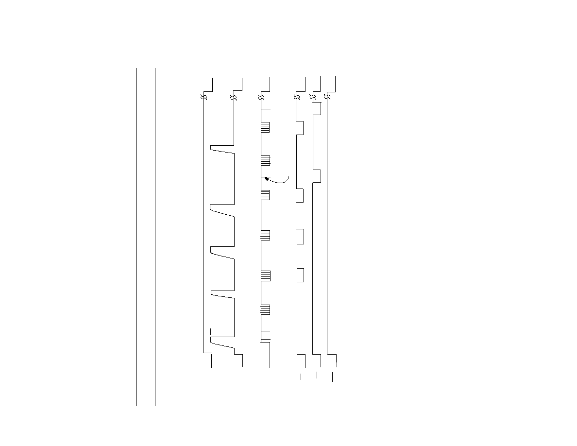
Figure 2. Programming Cycle Overview
RESET/OE
CE
CLK
V
PP
V
CC
V
PP1
V
PP2
V
CC =
V
CCP
Enter
Programming
Mode
Load Data
Word
Clock Increments
Address Counter
CEO
100
�
s
Programming
Pulse
500
�
s
Over Programming
Pulse
(Retry)
500
�
s
Programming
Pulse
(Retry)
100
�
s
Programming
Pulse
Verify Data
Word
Verify Data
Word
Verify Data
Word
Load Data
Word
Verify Data
Word

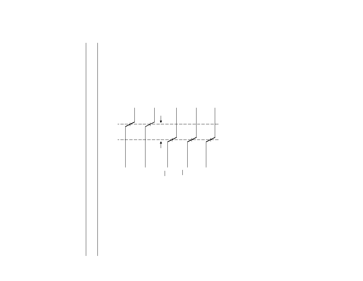
XILINX PROGRAMMER QUALIFICATION SPECIFICATION
XC17S00, & XC17S00XL
03/00 Rev. 2.1
12
V
CCP
V
PP1
V
CC
V
PP
CLK
DATA
CE
RESET/OE
V
PPNOM
V
PPNOM
T
RPP
T
SVC
T
FPP
T
HVC
T
SVC
2
4
5
1
4
Figure 3. Enter Programming Mode

XILINX PROGRAMMER QUALIFICATION SPECIFICATION
XC17S00, & XC17S00XL
03/00 Rev. 2.1
13
Increment
Word
Counter
1
2
Last Bit
V
PP1
6
8
7
CLK
DATA
V
PP
V
PP2
CE
RESET/OE
15
16
1
2
Last Bit
3
12
13
14
Program
Pulse
Load Prom Internal
Data Latches
Read Current Device Word
Figure 4. Details Of The Programming Cycle

XILINX PROGRAMMER QUALIFICATION SPECIFICATION
XC17S00, & XC17S00XL
03/00 Rev. 2.1
14
RESET/OE
CE
CLK
V
PP
V
CC
V
PP1
V
PPNOM
V
CCP
Enter
Programming
Mode
Load
Zeros **
Clock Increments
Address Counter *
CEO
* Number of Clocks for the Device Reset Polarity Location
5 ms
Programming
Reset Polarity
V
PP2
** Number of Clocks for the Device Word
(Reset active low)
(Reset active high-failed)
Figure 5. Programming Reset Polarity
XILINX PROGRAMMER QUALIFICATION SPECIFICATION
XC17S00, & XC17S00XL
03/00 Rev. 2.1
15
V
PP
RESET/OE
1 ms
GND
V
CC
V
PP2
V
CCP
GND
GND
GND
GND
CE
CLK
If your programming hardware does not allow V
PP
and V
CC
to power up and
down simultaneously, make sure to first power up V
PP
during power up and
power down V
PP
after V
CC
during power down.
Figure 6. Exit Programming Mode

XILINX PROGRAMMER QUALIFICATION SPECIFICATION
XC17S00, & XC17S00XL
03/00 Rev. 2.1
16
9
1
6
1
5
1
4
V
PP
CLK
DATA
CE
RESET/OE
1
2
3
Last Bit
V
PPVFY
V
CC
V
CCVFY
Verify CEO low one
clock after last bit
Read All Device Data Bits
CEO
(output)
(With Reset Polarity Bit unprogrammed, '1')
(With Reset Polarity Bit programmed, '0')
V
IH
(V
CCVFY
level)
V
IH
(V
CCVFY
level)
Figure 7. Details Of Verify Cycle