DS026 (v4.0) June 11, 2003
www.xilinx.com
1
Product Specification
1-800-255-7778
�2003 Xilinx, Inc. All rights reserved. All Xilinx trademarks, registered trademarks, patents, and further disclaimers are as listed at
http://www.xilinx.com/legal.htm
. All other
trademarks and registered trademarks are the property of their respective owners. All specifications are subject to change without notice.
NOTICE OF DISCLAIMER: Xilinx is providing this design, code, or information "as is." By providing the design, code, or information as one possible implementation of this fea-
ture, application, or standard, Xilinx makes no representation that this implementation is free from any claims of infringement. You are responsible for obtaining any rights you
may require for your implementation. Xilinx expressly disclaims any warranty whatsoever with respect to the adequacy of the implementation, including but not limited to any war-
ranties or representations that this implementation is free from claims of infringement and any implied warranties of merchantability or fitness for a particular purpose.
Features
�
In-system programmable 3.3V PROMs for
configuration of Xilinx FPGAs
-
Endurance of 20,000 program/erase cycles
-
Program/erase over full commercial/industrial
voltage and temperature range (�40�C to +85�C)
�
IEEE Std 1149.1 boundary-scan (JTAG) support
�
Simple interface to the FPGA
�
Cascadable for storing longer or multiple bitstreams
�
Low-power advanced CMOS FLASH process
�
Dual configuration modes
-
Serial Slow/Fast configuration (up to 33 MHz)
-
Parallel (up to 264 Mb/s at 33 MHz)
�
5V tolerant I/O pins accept 5V, 3.3V and 2.5V signals
�
3.3V or 2.5V output capability
�
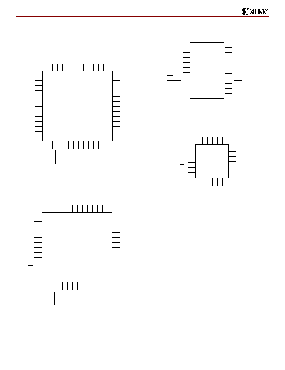
Available in PC20, SO20, PC44, and VQ44 packages
�
Design support using the Xilinx Alliance and
Foundation series software packages.
�
JTAG command initiation of standard FPGA
configuration
Description
Xilinx introduces the XC18V00 series of in-system program-
mable configuration PROMs (
Figure 1
). Devices in this 3.3V
family include a 4-megabit, a 2-megabit, a 1-megabit, and a
512-kilobit PROM that provide an easy-to-use, cost-effec-
tive method for re-programming and storing Xilinx FPGA
configuration bitstreams.
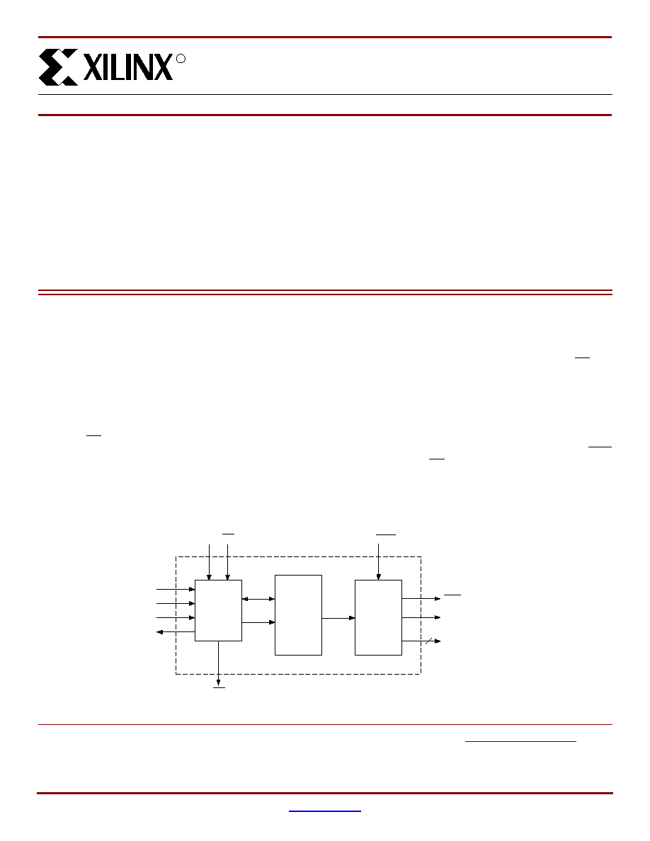
When the FPGA is in Master Serial mode, it generates a
configuration clock that drives the PROM. A short access
time after CE and OE are enabled, data is available on the
PROM DATA (D0) pin that is connected to the FPGA D
IN
pin. New data is available a short access time after each ris-
ing clock edge. The FPGA generates the appropriate num-
ber of clock pulses to complete the configuration. When the
FPGA is in Slave Serial mode, the PROM and the FPGA
are clocked by an external clock.
When the FPGA is in Master-SelectMAP mode, the FPGA
generates a configuration clock that drives the PROM.
When the FPGA is in Slave-Parallel or Slave-SelectMAP
Mode, an external oscillator generates the configuration
clock that drives the PROM and the FPGA. After CE and
OE are enabled, data is available on the PROMs DATA
(D0-D7) pins. New data is available a short access time
after each rising clock edge. The data is clocked into the
FPGA on the following rising edge of the CCLK. A free-run-
ning oscillator can be used in the Slave-Parallel or
Slave-SelecMAP modes.
Multiple devices can be concatenated by using the CEO
output to drive the CE input of the following device. The
clock inputs and the DATA outputs of all PROMs in this
chain are interconnected. All devices are compatible and
can be cascaded with other members of the family or with
the XC17V00 one-time programmable Serial PROM family.
0
XC18V00 Series In-System
Programmable Configuration
PROMs
DS026 (v4.0) June 11, 2003
0
0
Product Specification
R
Figure 1: XC18V00 Series Block Diagram
Control
and
JTAG
Interface
Memory
Serial
or
Parallel
Interface
D0 DATA
Serial or Parallel Mode
D[1:7]
Parallel Interface
Data
Address
CLK CE
TCK
TMS
TDI
TDO
OE/Reset
CEO
Data
DS026_01_090502
7
CF
XC18V00 Series In-System Programmable Configuration PROMs
2
www.xilinx.com
DS026 (v4.0) June 11, 2003
1-800-255-7778
Product Specification
R
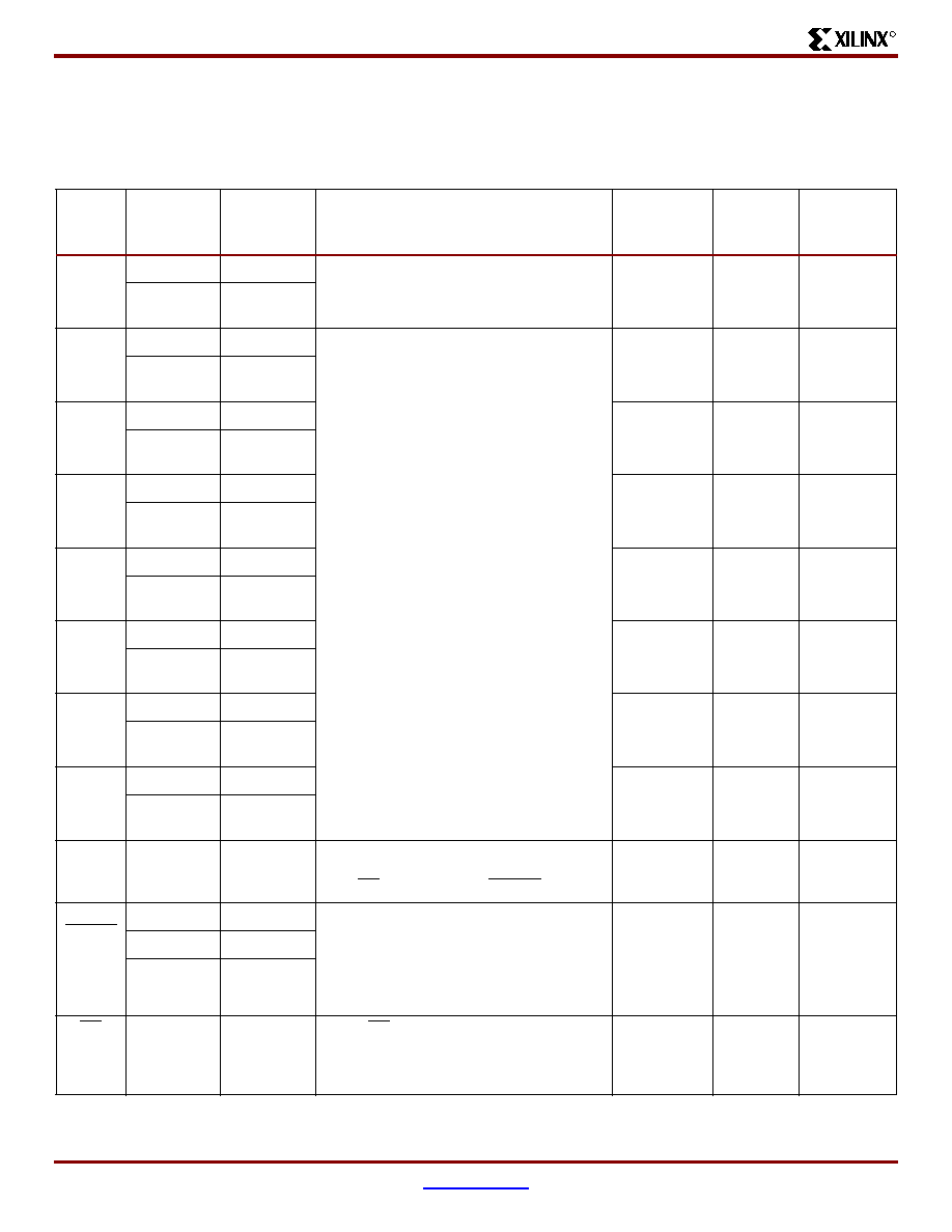
Pinout and Pin Description
Table 1
provides a list of the pin names and descriptions for the 44-pin VQFP and PLCC and the 20-pin SOIC and PLCC
packages.
Table 1: Pin Names and Descriptions
Pin
Name
Boundary
Scan
Order
Function
Pin Description
44-pin
VQFP
44-pin
PLCC
20-pin
SOIC &
PLCC
D0
4
DATA OUT
D0 is the DATA output pin to provide data
for configuring an FPGA in serial mode.
40
2
1
3
OUTPUT
ENABLE
D1
6
DATA OUT
D0-D7 are the output pins to provide
parallel data for configuring a Xilinx
FPGA in Slave-Parallel/SelectMap mode.
D1-D7 remain in HIGHZ state when the
PROM operates in serial mode.
D1-D7 can be left unconnected when the
PROM is used in serial mode.
29
35
16
5
OUTPUT
ENABLE
D2
2
DATA OUT
42
4
2
1
OUTPUT
ENABLE
D3
8
DATA OUT
27
33
15
7
OUTPUT
ENABLE
D4
24
DATA OUT
9
15
7
(1)
23
OUTPUT
ENABLE
D5
10
DATA OUT
25
31
14
9
OUTPUT
ENABLE
D6
17
DATA OUT
14
20
9
16
OUTPUT
ENABLE
D7
14
DATA OUT
19
25
12
13
OUTPUT
ENABLE
CLK
0
DATA IN
Each rising edge on the CLK input
increments the internal address counter if
both CE is Low and OE/RESET is High.
43
5
3
OE/
RESET
20
DATA IN
When Low, this input holds the address
counter reset and the DATA output is in a
high-impedance state. This is a
bidirectional open-drain pin that is held
Low while the PROM is reset. Polarity is
NOT programmable.
13
19
8
19
DATA OUT
18
OUTPUT
ENABLE
CE
15
DATA IN
When CE is High, the device is put into
low-power standby mode, the address
counter is reset, and the DATA pins are
put in a high-impedance state.
15
21
10
XC18V00 Series In-System Programmable Configuration PROMs
DS026 (v4.0) June 11, 2003
www.xilinx.com
3
Product Specification
1-800-255-7778
R
CF
22
DATA OUT
Allows JTAG CONFIG instruction to
initiate FPGA configuration without
powering down FPGA. This is an
open-drain output that is pulsed Low by
the JTAG CONFIG command.
10
16
7
(1)
21
OUTPUT
ENABLE
CEO
12
DATA OUT
Chip Enable Output (CEO) is connected
to the CE input of the next PROM in the
chain. This output is Low when CE is Low
and OE/RESET input is High, AND the
internal address counter has been
incremented beyond its Terminal Count
(TC) value. CEO returns to High when
OE/RESET goes Low or CE goes High.
21
27
13
11
OUTPUT
ENABLE
GND
GND is the ground connection.
6, 18, 28 &
41
3, 12, 24
& 34
11
TMS
MODE
SELECT
The state of TMS on the rising edge of
TCK determines the state transitions at
the Test Access Port (TAP) controller.
TMS has an internal 50K ohm resistive
pull-up on it to provide a logic "1" to the
device if the pin is not driven.
5
11
5
TCK
CLOCK
This pin is the JTAG test clock. It
sequences the TAP controller and all the
JTAG test and programming electronics.
7
13
6
TDI
DATA IN
This pin is the serial input to all JTAG
instruction and data registers. TDI has an
internal 50K ohm resistive pull-up on it to
provide a logic "1" to the system if the pin
is not driven.
3
9
4
TDO
DATA OUT
This pin is the serial output for all JTAG
instruction and data registers. TDO has
an internal 50K ohm resistive pull-up on it
to provide a logic "1" to the system if the
pin is not driven.
31
37
17
V
CCINT
Positive 3.3V supply voltage for internal
logic.
17, 35 &
38
(3)
23, 41 &
44
(3)
18 & 20
(3)
V
CCO
Positive 3.3V or 2.5V supply voltage
connected to the input buffers
(2)
and
output voltage drivers.
8, 16, 26 &
36
14, 22, 32
& 42
19
NC
No connects.
1, 2, 4,
11, 12, 20,
22, 23, 24,
30, 32, 33,
34, 37, 39,
44
1, 6, 7, 8,
10, 17, 18,
26, 28, 29,
30, 36, 38,
39, 40, 43
Notes:
1.
By default, pin 7 is the D4 pin in the 20-pin packages. However, CF --> D4 programming option can be set to override the default and route
the CF function to pin 7 in the Serial mode.
2.
For devices with IDCODES 0502x093h, the input buffers are supplied by V
CCINT
.
3.
For devices with IDCODES, 0503x093h, these V
CCINT
pins are no connects: pin 38 in 44-pin VQFP package, pin 44 in 44-pin PLCC
package and pin 20 in 20-pin SOIC and20-pin PLCC packages.
Table 1: Pin Names and Descriptions (Continued)
Pin
Name
Boundary
Scan
Order
Function
Pin Description
44-pin
VQFP
44-pin
PLCC
20-pin
SOIC &
PLCC