
1
Preliminary Product Specification
© 2005 Xilinx, Inc. All rights reserved. All Xilinx trademarks, registered trademarks, patents, and disclaimers are as listed at
http://www.xilinx.com/legal.htm
.
All other trademarks and registered trademarks are the property of their respective owners. All specifications are subject to change without notice.
Features
∑
Optimized for 1.8V systems
-
As fast as 5.7 ns pin-to-pin delays
-
As low as 13
µ
A quiescent current
∑
Industry's best 0.18 micron CMOS CPLD
-
Optimized architecture for effective logic synthesis.
Refer to the CoolRunnerTM-II family data sheet for
architecture description.
-
Multi-voltage I/O operation -- 1.5V to 3.3V
∑
Available in multiple package options
-
100-pin VQFP with 80 user I/O
-
144-pin TQFP with 118 user I/O
-
132-ball CP (0.5mm) BGA with 106 user I/O
-
208-pin PQFP with 173 user I/O
-
256-ball FT (1.0mm) BGA with 184 user I/O
-
Pb-free available for all packages
∑
Advanced system features
-
Fastest in system programming
∑
1.8V ISP using IEEE 1532 (JTAG) interface
-
IEEE1149.1 JTAG Boundary Scan Test
-
Optional Schmitt-trigger input (per pin)
-
Unsurpassed low power management
∑
DataGATE enable (DGE) signal control
-
Two separate I/O banks
-
RealDigital 100% CMOS product term generation
-
Flexible clocking modes
∑
Optional DualEDGE triggered registers
∑
Clock divider (divide by 2,4,6,8,10,12,14,16)
∑
CoolCLOCK
-
Global signal options with macrocell control
∑
Multiple global clocks with phase selection per
macrocell
∑
Multiple global output enables
∑
Global set/reset
-
Advanced design security
-
PLA architecture
∑
Superior pinout retention
∑
100% product term routability across function
block
-
Open-drain output option for Wired-OR and LED
drive
-
Optional bus-hold, 3-state or weak pull-up on
selected I/O pins
-
Optional configurable grounds on unused I/Os
-
Mixed I/O voltages compatible with 1.5V, 1.8V,
2.5V, and 3.3V logic levels
∑
SSTL2-1, SSTL3-1, and HSTL-1 I/O compatibility
-
Hot pluggable
Description
The CoolRunnerTM-II 256-macrocell device is designed for
both high performance and low power applications. This
lends power savings to high-end communication equipment
and high speed to battery operated devices. Due to the low
power stand-by and dynamic operation, overall system reli-
ability is improved
This device consists of sixteen Function Blocks inter-con-
nected by a low power Advanced Interconnect Matrix (AIM).
The AIM feeds 40 true and complement inputs to each
Function Block. The Function Blocks consist of a 40 by 56
P-term PLA and 16 macrocells which contain numerous
configuration bits that allow for combinational or registered
modes of operation.
Additionally, these registers can be globally reset or preset
and configured as a D or T flip-flop or as a D latch. There
are also multiple clock signals, both global and local product
term types, configured on a per macrocell basis. Output pin
configurations include slew rate limit, bus hold, pull-up,
open drain and programmable grounds. A Schmitt-trigger
input is available on a per input pin basis. In addition to stor-
ing macrocell output states, the macrocell registers may be
configured as "direct input" registers to store signals directly
from input pins.
Clocking is available on a global or Function Block basis.
Three global clocks are available for all Function Blocks as
a synchronous clock source. Macrocell registers can be
individually configured to power up to the zero or one state.
A global set/reset control line is also available to asynchro-
nously set or reset selected registers during operation.
Additional local clock, synchronous clock-enable, asynchro-
nous set/reset and output enable signals can be formed
using product terms on a per-macrocell or per-Function
Block basis.
A DualEDGE flip-flop feature is also available on a per mac-
rocell basis. This feature allows high performance synchro-
nous operation based on lower frequency clocking to help
reduce the total power consumption of the device.
Circuitry has also been included to divide one externally
supplied global clock (GCK2) by eight different selections.
This yields divide by even and odd clock frequencies.
The use of the clock divide (division by 2) and DualEDGE
flip-flop gives the resultant CoolCLOCK feature.
DataGATE is a method to selectively disable inputs of the
CPLD that are not of interest during certain points in time.
0
XC2C256 CoolRunner-II CPLD
DS094 (v2.7) March 7, 2005
0
0
Preliminary Product Specification
R
XC2C256 CoolRunner-II CPLD
DS094 (v2.7) March 7, 2005
Preliminary Product Specification
R
By mapping a signal to the DataGATE function, lower power
can be achieved due to reduction in signal switching.
Another feature that eases voltage translation is I/O bank-
ing. Two I/O banks are available on the CoolRunner-II 256
macrocell device that permit easy interfacing to 3.3V, 2.5V,
1.8V, and 1.5V devices.
The CoolRunner-II 256 macrocell CPLD is I/O compatible
with various I/O standards (see
Table 1
). This device is also
1.5V I/O compatible with the use of Schmitt-trigger inputs.
RealDigital Design Technology
Xilinx CoolRunner-II CPLDs are fabricated on a 0.18 micron
process technology which is derived from leading edge
FPGA product development. CoolRunner-II CPLDs employ
RealDigital, a design technique that makes use of CMOS
technology in both the fabrication and design methodology.
RealDigital design technology employs a cascade of CMOS
gates to implement sum of products instead of traditional
sense amplifier methodology. Due to this technology, Xilinx
CoolRunner-II CPLDs achieve both high-performance and
low power operation.
Supported I/O Standards
The CoolRunner-II 256 macrocell features LVCMOS,
LVTTL, SSTL and HSTL I/O implementations. See
Table 1
for I/O standard voltages. The LVTTL I/O standard is a gen-
eral purpose EIA/JEDEC standard for 3.3V applications that
use an LVTTL input buffer and Push-Pull output buffer. The
LVCMOS standard is used in 3.3V, 2.5V, 1.8V applications.
Both HSTL and SSTL I/O standards make use of a V
REF
pin
for JEDEC compliance. CoolRunner-II CPLDs are also 1.5V
I/O compatible with the use of Schmitt-trigger inputs
Table 1: I/O Standards for XC2C256
(1)
IOSTANDARD
Attribute
Output
V
CCIO
Input
V
CCIO
Input
V
REF
Board
Termination
Voltage V
TT
LVTTL
3.3
3.3
N/A
N/A
LVCMOS33
3.3
3.3
N/A
N/A
LVCMOS25
2.5
2.5
N/A
N/A
LVCMOS18
1.8
1.8
N/A
N/A
LVCMOS15
(2)
1.5
1.5
N/A
N/A
HSTL_1
1.5
1.5
0.75
0.75
SSTL2_1
2.5
2.5
1.25
1.25
SSTL3_1
3.3
3.3
1.5
1.5
(1)For information on Vref, see
XAPP399
.
(2) LVCMOS15 requires Schmitt-trigger inputs.
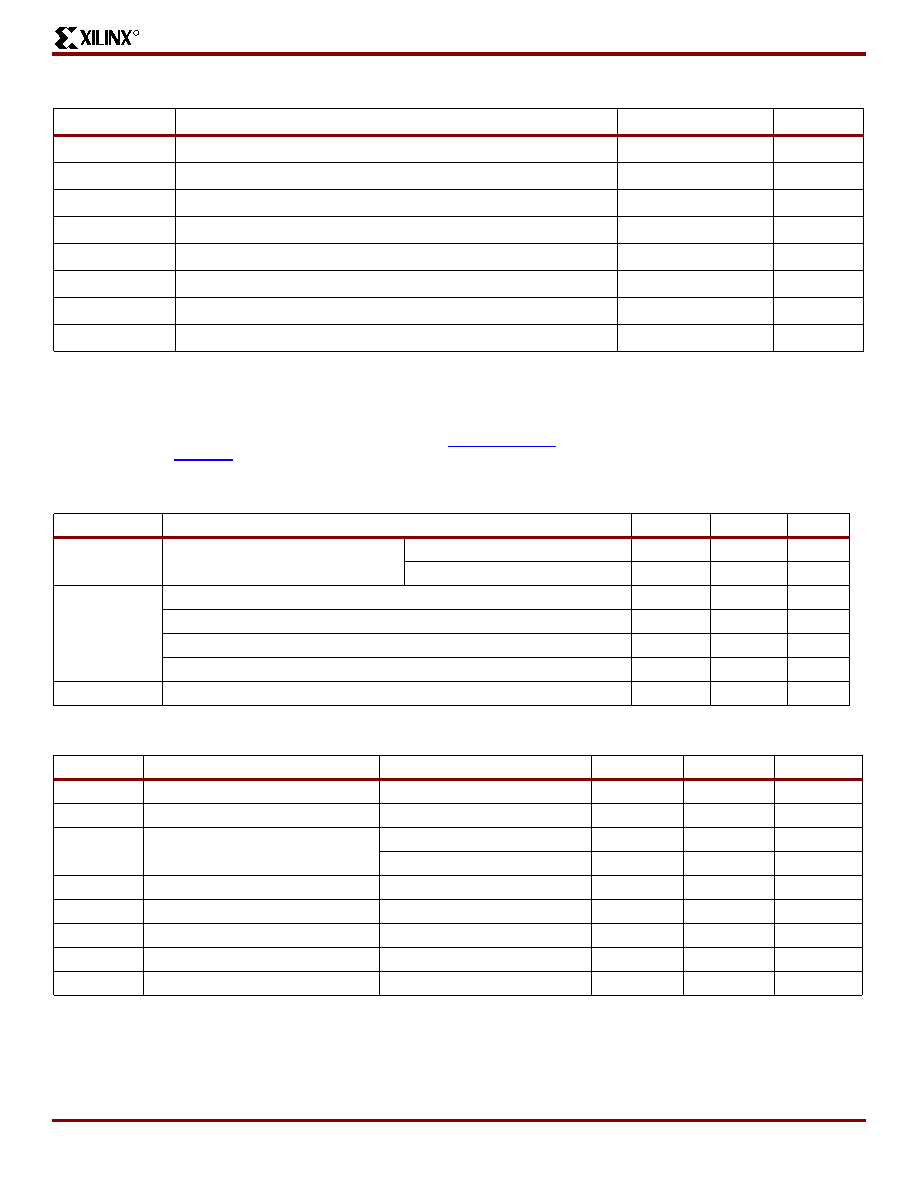
Figure 1: I
CC
vs Frequency
Table 2: I
CC
vs Frequency (LVCMOS 1.8V T
A
= 25∞C)
(1)
Frequency (MHz)
0
30
50
70
100
120
150
170
190
220
240
Typical I
CC
(mA)
0.021
11.68
19.40
27.01
38.18
45.54
56.32
63.37
70.40
80.90
88.03
Notes:
1.
16-bit up/down, resettable binary counter (one counter per function block).
Frequency (MHz)
I CC
(mA)
0
0
25
50
75
100
250
200
150
100
50
XC2C256 CoolRunner-II CPLD
3
Preliminary Product Specification
R
Recommended Operating Conditions
DC Electrical Characteristics
(Over Recommended Operating Conditions)
Absolute Maximum Ratings
Symbol
Description
Value
Units
V
CC
Supply voltage relative to ground
≠0.5 to 2.0
V
V
CCIO
Supply voltage for output drivers
≠0.5 to 4.0
V
V
JTAG
(2)
JTAG input voltage limits
≠0.5 to 4.0
V
V
AUX
JTAG input supply voltage
≠0.5 to 4.0
V
V
IN
(1)
Input voltage relative to ground
≠0.5 to 4.0
V
V
TS
(1)
Voltage applied to 3-state output
≠0.5 to 4.0
V
T
STG
(3)
Storage Temperature (ambient)
≠65 to +150
∞C
T
J
Junction Temperature
+150
∞C
Notes:
1.
Maximum DC undershoot below GND must be limited to either 0.5V or 10 mA, whichever is easiest to achieve. During transitions,
the device pins may undershoot to ≠2.0v or overshoot to +4.5V, provided this over or undershoot lasts less than 10 ns and with the
forcing current being limited to 200 mA.
2.
Valid over commercial temperature range.
3.
For soldering guidelines and thermal considerations, see the
Device Packaging
information on the Xilinx website. For Pb free
packages, see
XAPP427
.
Symbol
Parameter
Min
Max
Units
V
CC
Supply voltage for internal logic
and input buffers
Commercial T
A
= 0∞C to +70∞C
1.7
1.9
V
Industrial T
A
= ≠40∞C to +85∞C
1.7
1.9
V
V
CCIO
Supply voltage for output drivers @ 3.3V operation
3.0
3.6
V
Supply voltage for output drivers @ 2.5V operation
2.3
2.7
V
Supply voltage for output drivers @ 1.8V operation
1.7
1.9
V
Supply voltage for output drivers @ 1.5V operation
1.4
1.6
V
V
AUX
JTAG programming
1.7
3.6
V
Symbol
Parameter
Test Conditions
Typical
Max.
Units
I
CCSB
Standby current Commercial
V
CC
= 1.9V, V
CCIO
= 3.6V
33
150
µ
A
I
CCSB
Standby current Industrial
V
CC
= 1.9V, V
CCIO
= 3.6V
54
300
µ
A
I
CC
Dynamic current
f = 1 MHz
-
410
µ
A
f = 50 MHz
-
27
mA
C
JTAG
JTAG input capacitance
f = 1 MHz
-
10
pF
C
CLK
Global clock input capacitance
f = 1 MHz
-
12
pF
C
IO
I/O capacitance
f = 1 MHz
-
10
pF
I
IL
(2)
Input leakage current
V
IN
= 0V or V
CCIO
to 3.9V
-
+/≠1
µ
A
I
IH
(2)
I/O High-Z leakage
V
IN
= 0V or V
CCIO
to 3.9V
-
+/≠1
µ
A
Notes:
1.
16-bit up/down, resettable binary counter (one counter per function block) tested at
V
CC
= V
CCIO
= 1.9V
2.
See Quality and Reliability section of the CoolRunner-II family data sheet
XC2C256 CoolRunner-II CPLD
DS094 (v2.7) March 7, 2005
Preliminary Product Specification
R
LVCMOS 3.3V and LVTTL 3.3V DC Voltage Specifications
LVCMOS 2.5V DC Voltage Specifications
LVCMOS 1.8V DC Voltage Specifications
LVCMOS
1.5V DC Voltage Specifications
(1)
Symbol
Parameter
Test Conditions
Min.
Max.
Units
V
CCIO
Input source voltage
-
3.0
3.6
V
V
IH
High level input voltage
-
2
3.9
V
V
IL
Low level input voltage
-
≠0.3
0.8
V
V
OH
High level output voltage
I
OH
= ≠8 mA, V
CCIO
= 3V
V
CCIO
≠ 0.4V
-
V
I
OH
= ≠0.1 mA, V
CCIO
= 3V
V
CCIO
≠ 0.2V
-
V
V
OL
Low level output voltage
I
OL
= 8 mA, V
CCIO
= 3V
-
0.4
V
I
OL
= 0.1 mA, V
CCIO
= 3V
-
0.2
V
Symbol
Parameter
Test Conditions
Min.
Max.
Units
V
CCIO
Input source voltage
-
2.3
2.7
V
V
IH
High level input voltage
-
1.7
3.9
V
V
IL
Low level input voltage
-
≠0.3
0.7
V
V
OH
High level output voltage
I
OH
= ≠8 mA, V
CCIO
= 2.3V
V
CCIO
≠ 0.4V
-
V
I
OH
= ≠0.1 mA, V
CCIO
= 2.3V
V
CCIO
≠ 0.2V
-
V
V
OL
Low level output voltage
I
OL
= 8 mA, V
CCIO
= 2.3V
-
0.4
V
I
OL
= 0.1 mA, V
CCIO
= 2.3V
-
0.2
V
Symbol
Parameter
Test Conditions
Min.
Max.
Units
V
CCIO
Input source voltage
-
1.7
1.9
V
V
IH
High level input voltage
-
0.65 x V
CCIO
3.9
V
V
IL
Low level input voltage
-
≠0.3
0.35 x V
CCIO
V
V
OH
High level output voltage
I
OH
= ≠8 mA, V
CCIO
= 1.7V
V
CCIO
≠ 0.45
-
V
I
OH
= ≠0.1 mA, V
CCIO
= 1.7V
V
CCIO
≠ 0.2
-
V
V
OL
Low level output voltage
I
OL
= 8 mA, V
CCIO
= 1.7V
-
0.45
V
I
OL
= 0.1 mA, V
CCIO
= 1.7V
-
0.2
V
Symbol
Parameter
Test Conditions
Min.
Max.
Units
V
CCIO
Input source voltage
-
1.4
1.6
V
V
T+
Input hysteresis threshold voltage
-
0.5 x V
CCIO
0.8 x V
CCIO
V
V
T-
-
0.2
x
V
CCIO
0.5 x V
CCIO
V
V
OH
High level output voltage
I
OH
= ≠8 mA, V
CCIO
= 1.4V
V
CCIO
≠ 0.45
-
V
I
OH
= ≠0.1 mA, V
CCIO
= 1.4V
V
CCIO
≠ 0.2
-
V
XC2C256 CoolRunner-II CPLD
5
Preliminary Product Specification
R
Schmitt Trigger Input DC Voltage Specifications
SSTL2-1 DC Voltage Specifications
V
OL
Low level output voltage
I
OL
= 8 mA, V
CCIO
= 1.4V
-
0.4
V
I
OL
= 0.1 mA, V
CCIO
= 1.4V
-
0.2
V
Notes:
1.
Hysteresis used on 1.5V inputs.
Symbol
Parameter
Test Conditions
Min.
Max.
Units
V
CCIO
Input source voltage
-
1.4
3.9
V
V
T+
Input hysteresis threshold voltage
-
0.5 x V
CCIO
0.8 x V
CCIO
V
V
T-
-
0.2
x
V
CCIO
0.5 x V
CCIO
V
Symbol
Parameter
Test Conditions
Min.
Typ
Max.
Units
V
CCIO
Input source voltage
-
2.3
2.5
2.7
V
V
REF
(1)
Input reference voltage
-
1.15
1.25
1.35
V
V
TT
(2)
Termination voltage
-
V
REF
≠ 0.04
1.25
V
REF
+ 0.04
V
V
IH
High level input voltage
-
V
REF
+ 0.18
-
3.9
V
V
IL
Low level input voltage
-
≠0.3
-
V
REF
≠ 0.18
V
V
OH
High level output voltage
I
OH
= ≠8 mA, V
CCIO
= 2.3V
V
CCIO
≠ 0.62
-
-
V
V
OL
Low level output voltage
I
OL
= 8 mA, V
CCIO
= 2.3V
-
-
0.54
V
Notes:
1.
V
REF
should track the variations in V
CCIO
, also peak to peak AC noise on V
REF
may not exceed ± 2% V
REF
2.
V
TT
of transmitting device must track V
REF
of receiving devices
Symbol
Parameter
Test Conditions
Min.
Max.
Units