 | –≠–ª–µ–∫—Ç—Ä–æ–Ω–Ω—ã–π –∫–æ–º–ø–æ–Ω–µ–Ω—Ç: XC2C64 | –°–∫–∞—á–∞—Ç—å:  PDF PDF  ZIP ZIP |
DS090 (v2.5) June 28, 2005
www.xilinx.com
1
Product Specification
© 2005 Xilinx, Inc. All rights reserved. All Xilinx trademarks, registered trademarks, patents, and disclaimers are as listed at
http://www.xilinx.com/legal.htm
.
All other trademarks and registered trademarks are the property of their respective owners. All specifications are subject to change without notice.
Features
∑
Optimized for 1.8V systems
-
Industry's fastest low power CPLD
-
Densities from 32 to 512 macrocells
∑
Industry's best 0.18 micron CMOS CPLD
-
Optimized architecture for effective logic synthesis
-
Multi-voltage I/O operation -- 1.5V to 3.3V
∑
Advanced system features
-
Fastest in system programming
∑
1.8V ISP using IEEE 1532 (JTAG) interface
-
On-The-Fly Reconfiguration (OTF)
-
IEEE1149.1 JTAG Boundary Scan Test
-
Optional Schmitt trigger input (per pin)
-
Multiple I/O banks on all devices
-
Unsurpassed low power management
∑
DataGATE external signal control
-
Flexible clocking modes
∑
Optional DualEDGE triggered registers
∑
Clock divider (
˜
2,4,6,8,10,12,14,16)
∑
CoolCLOCK
-
Global signal options with macrocell control
∑
Multiple global clocks with phase selection per
macrocell
∑
Multiple global output enables
∑
Global set/reset
-
Abundant product term clocks, output enables and
set/resets
-
Efficient control term clocks, output enables and
set/resets for each macrocell and shared across
function blocks
-
Advanced design security
-
Open-drain output option for Wired-OR and LED
drive
-
Optional bus-hold, 3-state or weak pullup on select
I/O pins
-
Optional configurable grounds on unused I/Os
-
Mixed I/O voltages compatible with 1.5V, 1.8V,
2.5V, and 3.3V logic levels on all parts
-
SSTL2_1,SSTL3_1, and HSTL_1 on 128
macrocell and denser devices
-
Hot pluggable
∑
PLA architecture
-
Superior pinout retention
-
100% product term routability across function block
∑
Wide package availability including fine pitch:
-
Chip Scale Package (CSP) BGA, Fine Line BGA,
TQFP, PQFP, VQFP, PLCC, and QFN packages
-
Pb-free available for all packages
∑
Design entry/verification using Xilinx and industry
standard CAE tools
∑
Free software support for all densities using Xilinx
WebPACKTM
∑
Industry leading nonvolatile 0.18 micron CMOS
process
-
Guaranteed 1,000 program/erase cycles
-
Guaranteed 20 year data retention
Family Overview
Xilinx CoolRunnerTM-II CPLDs deliver the high speed and
ease of use associated with the XC9500/XL/XV CPLD fam-
ily with the extremely low power versatility of the XPLA3TM
family in a single CPLD. This means that the exact same
parts can be used for high-speed data communications/
computing systems and leading edge portable products,
with the added benefit of In System Programming. Low
power consumption and high-speed operation are com-
bined into a single family that is easy to use and cost effec-
tive. Clocking techniques and other power saving features
extend the users' power budget. The design features are
supported starting with Xilinx ISE 4.1i ISE WebPACK. Addi-
tional details can be found in
Further Reading, page 13
.
Table 1
shows the macrocell capacity and key timing
parameters for the CoolRunner-II CPLD family.
0
CoolRunner-II CPLD Family
DS090 (v2.5) June 28, 2005
0
0
Product Specification
R
Table 1: CoolRunner-II CPLD Family Parameters
XC2C32A
XC2C64A
XC2C128
XC2C256
XC2C384
XC2C512
Macrocells
32
64
128
256
384
512
Max I/O
33
64
100
184
240
270
T
PD
(ns)
3.8
4.6
5.7
5.7
7.1
7.1
T
SU
(ns)
1.9
2.0
2.4
2.4
2.9
2.6
T
CO
(ns)
3.7
3.9
4.2
4.5
5.8
5.8
F
SYSTEM1
(MHz)
323 263 244
256 217 179
CoolRunner-II CPLD Family
2
www.xilinx.com
DS090 (v2.5) June 28, 2005
Product Specification
R
Table 2
shows key DC characteristics for the CoolRunner-II
family.
Table 3
shows the CoolRunner-II CPLD package offering
with corresponding I/O count. All packages are surface
mount, with over half of them being ball-grid technologies.
The ultra tiny packages permit maximum functional capacity
in the smallest possible area. The CMOS technology used
in CoolRunner-II CPLDs generates minimal heat, allowing
the use of tiny packages during high-speed operation.
With the exception of the new Pb-free QF packages, there
are at least two densities present in each package with
three in the VQ100 (100-pin 1.0mm QFP) and TQ144
(144-pin 1.4mm QFP), and in the FT256 (256-ball 1.0mm
spacing FLBGA). The FT256 is particularly important for
slim dimensioned portable products with mid- to high-den-
sity logic requirements.
Table 4
details the distribution of advanced features across
the CoolRunner-II CPLD family. The family has uniform
basic features with advanced features included in densities
where they are most useful. For example, it is very unlikely
that four I/O banks are needed on 32 and 64 macrocell
parts, but very likely they are for 384 and 512 macrocell
parts. The I/O banks are groupings of I/O pins using any
one of a subset of compatible voltage standards that share
the same V
CCIO
level. (See
Table 5
for a summary of
CoolRunner-II I/O standards.)
Table 2: CoolRunner-II CPLD DC Characteristics
XC2C32A
XC2C64A
XC2C128
XC2C256
XC2C384
XC2C512
I
CC
(
µ
A), 0 MHz, 25∞C (typical)
16
17
19
21
23
25
I
CC
(mA), 50 MHz, 70∞C (max)
2.5
5
10
27
45
55
I
CC
is dynamic current.
Table 3: CoolRunner-II CPLD Family Packages and I/O Count
XC2C32
XC2C32A
XC2C64
XC2C64A
XC2C128
XC2C256
XC2C384
XC2C512
QFG32
(1)
21
-
-
-
-
-
-
PC44
33
33
33
33
-
-
-
-
PCG44
(1)
33
33
-
-
-
-
VQ44
33
33
33
33
-
-
-
-
VQG44
(1)
33
33
-
-
-
-
QFG48
(1)
-
-
-
37
-
-
-
-
CP56
33
33
45
45
-
-
-
-
CPG56
(1)
33
45
-
-
-
-
VQ100
-
-
64
64
80
80
-
-
VQG100
(1)
-
-
64
80
80
-
-
CP132
-
-
-
-
100
106
-
-
CPG132
(1)
-
-
-
-
100
106
-
-
TQ144
-
-
-
-
100
118
118
-
TQG144
(1)
-
-
-
-
100
118
118
-
PQ208
-
-
-
-
-
173
173
173
PQG208
(1)
-
-
-
-
-
173
173
173
FT256
-
-
-
-
-
184
212
212
FTG256
(1)
-
-
-
-
-
184
212
212
FG324
-
-
-
-
-
-
240
270
FGG324
(1)
-
-
-
-
-
-
240
270
Notes:
1.
The letter "G" as the third character indicates a Pb-free package.

CoolRunner-II CPLD Family
DS090 (v2.5) June 28, 2005
www.xilinx.com
3
Product Specification
R
Architecture Description
CoolRunner-II CPLD is a highly uniform family of fast, low
power CPLDs. The underlying architecture is a traditional
CPLD architecture combining macrocells into Function
Blocks (FBs) interconnected with a global routing matrix,
the Xilinx Advanced Interconnect Matrix (AIM). The Func-
tion Blocks use a Programmable Logic Array (PLA) config-
uration which allows all product terms to be routed and
shared among any of the macrocells of the FB. Design soft-
ware can efficiently synthesize and optimize logic that is
subsequently fit to the FBs and connected with the ability to
utilize a very high percentage of device resources. Design
changes are easily and automatically managed by the soft-
ware, which exploits the 100% routability of the Program-
mable Logic Array within each FB. This extremely robust
building block delivers the industry's highest pinout reten-
tion, under very broad design conditions. The architecture
will be explained by expanding the detail as we discuss the
underlying Function Blocks, logic and interconnect.
The design software automatically manages these device
resources so that users can express their designs using
completely generic constructs without knowledge of these
architectural details. More advanced users can take advan-
tage of these details to more thoroughly understand the
software's choices and direct its results.
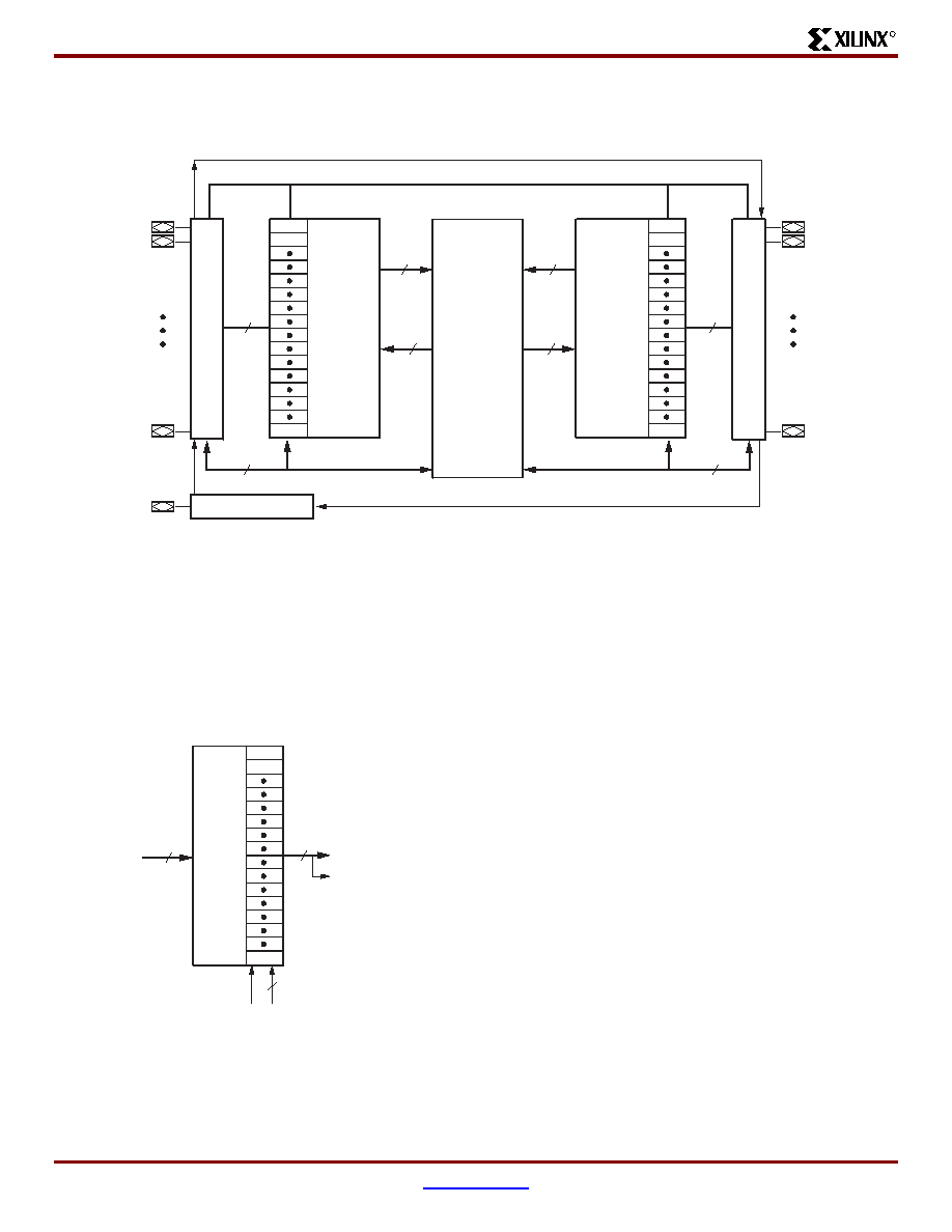
Figure 1
shows the high-level architecture whereby Func-
tion Blocks attach to pins and interconnect to each other
within the internal interconnect matrix. Each FB contains 16
macrocells. The BSC path is the JTAG Boundary Scan Con-
Table 4: CoolRunner-II CPLD Family Features
XC2C32
XC2C32A
XC2C64
XC2C64A
XC2C128
XC2C256
XC2C384
XC2C512
IEEE 1532
I/O banks
1
2
1
2
2
2
4
4
Clock division
-
-
-
-
DualEDGE Registers
DataGATE
-
-
-
-
LVTTL
LVCMOS33, 25, 18,
and 15
(1)
SSTL2_1
-
-
-
-
SSTL3_1
-
-
-
-
HSTL_1
-
-
-
-
Configurable ground
Quadruple data
security
Open drain outputs
Hot plugging
Schmitt Inputs
(1) LVCMOS15 requires the use of Schmitt-trigger inputs.
CoolRunner-II CPLD Family
4
www.xilinx.com
DS090 (v2.5) June 28, 2005
Product Specification
R
trol path. The BSC and ISP block has the JTAG controller
and In-System Programming Circuits.
Function Block
The CoolRunner-II CPLD Function Blocks contain 16 mac-
rocells, with 40 entry sites for signals to arrive for logic cre-
ation and connection. The internal logic engine is a 56
product term PLA. All Function Blocks, regardless of the
number contained in the device, are identical. For a
high-level view of the Function Block, see
Figure 2
.
At the high level, it is seen that the product terms (p-terms)
reside in a programmable logic array (PLA). This structure
is extremely flexible, and very robust when compared to
fixed or cascaded product term function blocks.
Classic CPLDs typically have a few product terms available
for a high-speed path to a given macrocell. They rely on
capturing unused p-terms from neighboring macrocells to
expand their product term tally, when needed. The result of
this architecture is a variable timing model and the possibil-
ity of stranding unusable logic within the FB.
The PLA is different -- and better. First, any product term
can be attached to any OR gate inside the FB macrocell(s).
Second, any logic function can have as many p-terms as
needed attached to it within the FB, to an upper limit of 56.
Third, product terms can be re-used at multiple macrocell
OR functions so that within a FB, a particular logical product
need only be created once, but can be re-used up to 16
times within the FB. Naturally, this plays well with the fitting
software, which identifies product terms that can be shared.
The software places as many of those functions as it can
into FBs, so it happens for free. There is no need to force
macrocell functions to be adjacent or any other restriction
save residing in the same FB, which is handled by the soft-
ware. Functions need not share a common clock, common
set/reset or common output enable to take full advantage of
the PLA. Also, every product term arrives with the same
time delay incurred. There are no cascade time adders for
putting more product terms in the FB. When the FB product
term budget is reached, there is a small interconnect timing
penalty to route signals to another FB to continue creating
logic. Xilinx design software handles all this automatically.
Figure 1: CoolRunner-II CPLD Architecture
Function
Block 1
Function
Block n
PLA
PLA
I/O Blocks
I/O Blocks
16
16
40
40
16 FB
16 FB
16
16
I/O Pin
MC1
MC2
MC16
MC1
MC2
MC16
DS090_01_121201
AIM
I/O Pin
I/O Pin
Direct Inputs
BSC and ISP
Clock and Control Signals
BSC Path
Direct Inputs
I/O Pin
I/O Pin
I/O Pin
JTAG
Figure 2: CoolRunner-II CPLD Function Block
PLA
16
40
3
MC1
Out
To AIM
Global
Clocks
Global
Set/Reset
MC2
MC16
DS090_02_101001

CoolRunner-II CPLD Family
DS090 (v2.5) June 28, 2005
www.xilinx.com
5
Product Specification
R
Macrocell
The CoolRunner-II CPLD macrocell is extremely efficient
and streamlined for logic creation. Users can develop sum
of product (SOP) logic expressions that comprise up to 40
inputs and span 56 product terms within a single function
block. The macrocell can further combine the SOP expres-
sion into an XOR gate with another single p-term expres-
sion. The resulting logic expression's polarity is also
selectable. As well, the logic function can be pure combina-
torial or registered, with the storage element operating
selectably as a D or T flip-flop, or transparent latch. Avail-
able at each macrocell are independent selections of glo-
bal, function block level or local p-term derived clocks, sets,
resets, and output enables. Each macrocell flip-flop is con-
figurable for either single edge or DualEDGE clocking, pro-
viding either double data rate capability or the ability to
distribute a slower clock (thereby saving power). For single
edge clocking or latching, either clock polarity may be
selected per macrocell. CoolRunner-II macrocell details are
shown in
Figure 3
. Note that in
Figure 4
, standard logic
symbols are used except the trapezoidal multiplexers have
input selection from statically programmed configuration
select lines (not shown). Xilinx application note XAPP376
gives a detailed explanation of how logic is created in the
CoolRunner-II CPLD family.
When configured as a D-type flip-flop, each macrocell has
an optional clock enable signal permitting state hold while a
clock runs freely. Note that Control Terms (CT) are available
to be shared for key functions within the FB, and are gener-
ally used whenever the exact same logic function would be
repeatedly created at multiple macrocells. The CT product
terms are available for FB clocking (CTC), FB asynchro-
nous set (CTS), FB asynchronous reset (CTR), and FB out-
put enable (CTE).
Any macrocell flip-flop can be configured as an input regis-
ter or latch, which takes in the signal from the macrocell's
I/O pin, and directly drives the AIM. The macrocell combina-
tional functionality is retained for use as a buried logic node
if needed. F
Toggle
is the maximum clock frequency to which
a T flip-flop can reliably toggle.
Advanced Interconnect Matrix (AIM)
The Advanced Interconnect Matrix is a highly connected
low power rapid switch. The AIM is directed by the software
to deliver up to a set of 40 signals to each FB for the cre-
ation of logic. Results from all FB macrocells, as well as, all
pin inputs circulate back through the AIM for additional con-
nection available to all other FBs as dictated by the design
Figure 3: CoolRunner-II CPLD Macrocell
GCK0
GCK1
GCK2
CTC
PTC
PTC
DS090_03_121201
49 P-terms
To PTA, PTB, PTC of
other macrocells
CTC, CTR,
CTS, CTE
From AIM
4 P-terms
PTA
Direct Input
from
I/O Block
Feedback
to AIM
PTB
PTC
PLA OR Term
PTA
CTS
GSR
GND
GND
V
CC
R
D/T
CE
CK
FIF
Latch
DualEDGE
Q
S
40
To I/O Block
PTA
CTR
GSR
GND