DS092 (v1.0) December 19, 2001
www.xilinx.com
1
Advance Product Specification
1-800-255-7778
© 2001 Xilinx, Inc. All rights reserved. All Xilinx trademarks, registered trademarks, patents, and disclaimers are as listed at
http://www.xilinx.com/legal.htm
.
All other trademarks and registered trademarks are the property of their respective owners. All specifications are subject to change without notice.
Features
∑
Industries best 0.18 micron CMOS CPLD
-
4.0 ns pin-to-pin logic delays
-
less than 100
µ
A standby current consumption
-
64 macrocells with up to 1,600 logic gates
-
Fast input registers
-
Slew rate control on individual outputs
-
LVCMOS 1.8V through 3.3V
-
LVTTL 3.3V
∑
Available in multiple package styles
-
44-pin PLCC with 33 user I/O
-
44-pin VQFP with 33 user I/O
-
56-ball CP (0.05mm) BGA with 45 user I/O
-
100-pin VQFP with 64 user I/O
∑
Optimized for high performance 1.8V systems
-
Ultra low power operation
-
Advanced 0.18 micron 4-metal layer Non-volatile
process
∑
Advanced system features
-
Quadruple enhanced security
-
Multi-voltage system interface
-
Hot pluggable
-
IEEE1532 In-system programmable
-
Superior pin locking through PLA array
-
Input hysteresis (Schmitt trigger) on all pins
-
Bus hold circuitry on all user pins
-
IEEE standard 1149.1 boundary scan (JTAG)
-
Fast programming times
-
Excellent pin retention during design changes
-
High quality and reliability
-
Guaranteed 10,000 program/erase cycles
-
20 year data retention
Refer to the CoolRunnerTM-II family data sheet for architec-
ture description.
Description
The CoolRunner-II 64-macrocell device is designed for both
high performance and low power applications. This lends
power savings to high-end communication equipment and
speed to battery operated devices.
This device consists of four Function Blocks inter-con-
nected by a low power Advanced Interconnect Matrix (AIM).
The AIM feeds 40 inputs to each Function Block. The Func-
tion Blocks consist of a 40 by 56 p-term PLA and 16 macro-
cells which contain numerous configuration bits that allow
for combinational or registered modes of operation. Addi-
tionally, these registers can be globally reset or preset and
configured as a D or T flip-flop or as a D latch. There are
also multiple clock signals, both global and local product
term based, on a per macrocell basis. Output control sig-
nals include slew rate control, bus hold and open drain. An
additional Schmitt-trigger input is available on a per input
pin basis.
In addition to combinatorial and registered outputs, the reg-
isters may be configured as fast inputs.
Clocking is available on a global or Function Block basis.
Three global clocks are available for all Function Blocks as
a synchronous clock source. Global clocks are additionally
used to set or preset individual macrocell registers on
power up. Local clocks are generated in specific Function
Blocks and only available to macrocell registers in that
Function Block.
A DualEDGE flip-flop feature is also available on a per mac-
rocell basis. This feature allows performance where it is
needed without raising the total power consumption of the
entire device.
The CoolRunner-II 64-macrocell CPLD is I/O compatible
with standard LVTTL33 and LVCMOS18, 25, and 33 volts
(see Table 1).
Fast Zero Power Design Technology
All CoolRunner-II CPLDs employ Fast Zero PowerTM (FZP),
a design technique that employs CMOS technology in both
the fabrication and design methodology. Xilinx CoolRun-
ner-II is fabricated on a 0.18 micron process technology
which is derived from leading edge FPGA product develop-
ment. CoolRunner-II design technology employs a cascade
of CMOS gates to implement sum of products instead of tra-
ditional sense amplifier methodology. Due to this FZP tech-
nology, Xilinx CoolRunner-II CPLDs achieve both high
performance and low power operation.
0
XC2C64 CoolRunner-II CPLD
DS092 (v1.0) December 19, 2001
0
0
Advance Product Specification
R
XC2C64 CoolRunner-II CPLD
2
www.xilinx.com
DS092 (v1.0) December 19, 2001
1-800-255-7778
Advance Product Specification
R
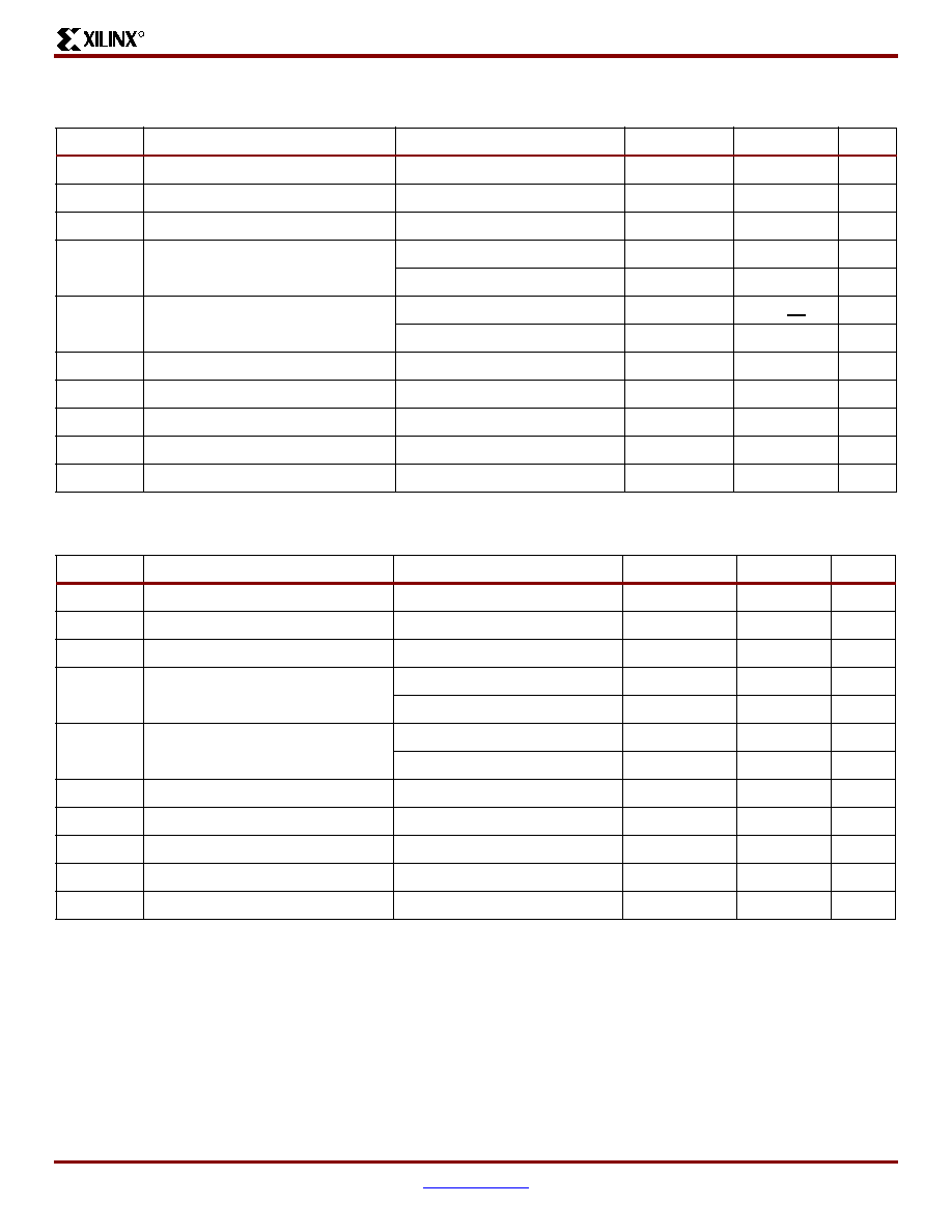
Supported I/O Standards
The CoolRunner-II 64 macrocell features both LVCMOS
and LVTTL I/O implementations. See
Table 1
for I/O stan-
dard voltages. The LVTTL I/O standard is a general purpose
EIA/JESDSA standard for 3.3V applications that use an
LVTTL input buffer and Push-Pull output buffer. The LVC-
MOS standard is used in 3.3V, 2.5V, 1.8V, and 1.5V applica-
tions. It does not require the use of a reference voltage or
termination voltage.
Table 1: I/O Standards for XC2C64
I/O
Standard
Output
V
CCIO
Input
V
CCIO
Input
V
REF
Board
Termination
Voltage V
T
LVTTL
3.3V
3.3V
N/A
N/A
LVCMOS33
3.3
3.3
N/A
N/A
LVCMOS25
2.5
2.5
N/A
N/A
LVCMOS18
1.8
1.8
N/A
N/A
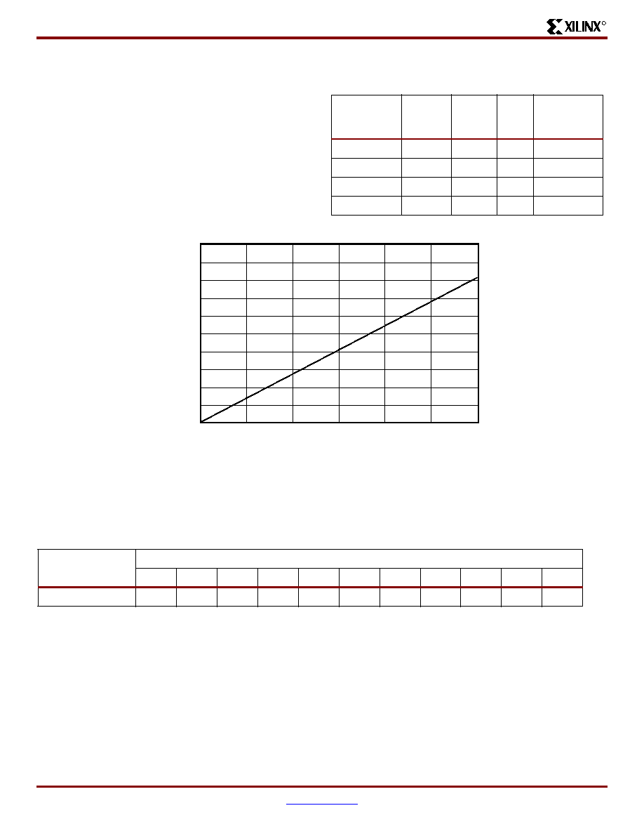
Figure 1: I
CC
vs Frequency
Table 2: I
CC
vs Frequency (LVCMOS 1.8V T
A
= 25∞C)
Frequency (MHz)
50
75
100
125
150
175
200
225
250
275
300
Typical I
CC
(mA)
3.6
5.5
7.3
9.1
10.8
12.5
14.2
15.9
17.5
19.2
20.8
Frequency (MHz)
DS092_07_121501
I CC
(mA)
0
0
5
10
15
20
25
300
250
200
150
100
50
XC2C64 CoolRunner-II CPLD
DS092 (v1.0) December 19, 2001
www.xilinx.com
3
Advance Product Specification
1-800-255-7778
R
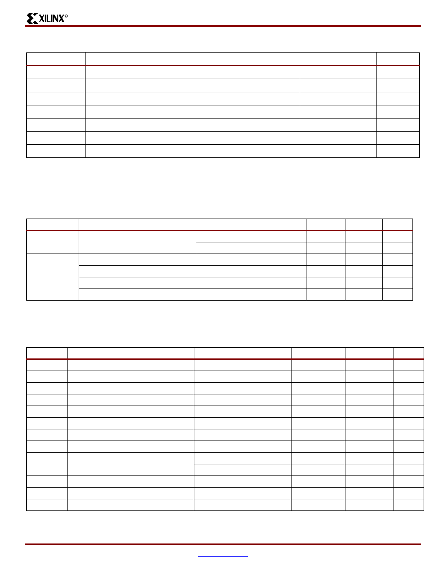
Recommended Operating Conditions
DC Electrical Characteristics
(Over Recommended Operating Conditions)
Absolute Maximum Ratings
Symbol
Description
Value
Units
V
CC
Supply voltage relative to ground
≠0.5 to 2.0
V
V
CCIO
Supply voltage for output drivers
≠0.5 to 4.0
V
V
IN
Input voltage relative to ground
(1)
≠0.5 to 4.0
V
V
TS
Voltage applied to 3-state output
(1)
≠0.5 to 4.0
V
V
STG
Storage Temperature (ambient)
≠65 to +150
∞C
T
SOL
Maximum Soldering temperature (10s @ 1/16in. = 1.5mm)
+ 60
∞C
T
J
Junction Temperature
+ 50
∞C
Notes:
1.
Maximum DC undershoot below GND must be limited to either 0.5V or 10 mA, whichever is easiest to achieve. During transitions,
the device pins may undershoot to ≠2.0v or overshoot to +3.9V, provided this over or undershoot lasts less than 10 ns and with the
forcing current being limited to 200 mA.
Symbol
Parameter
Min
Max
Units
V
CC
Supply voltage for internal logic
and input buffers
Commercial T
A
= 0∞C to +70∞C
1.7
1.9
V
Industrial T
A
= ≠40∞C to +85∞C
1.7
1.9
V
V
CCIO
Supply voltage for output drivers @ 3.3V operation
3.0
3.6
V
Supply voltage for output drivers @ 2.5V operation
2.3
2.7
V
Supply voltage for output drivers @ 1.8V operation
1.7
1.9
V
Supply voltage for output drivers @ 1.5V operation
(1)
1.4
1.6
V
Notes:
1.
Use input hysteresis for 1.5V LVCMOS.
Symbol
Parameter
Test Conditions
Min.
Max.
Units
V
CCIO
Input source voltage
3.0
3.6
V
V
IH
High level input voltage
2.0
V
CCIO
+ 0.3V
V
V
IL
Low level input voltage
≠0.3
0.8
V
V
OH
High level output voltage
I
OH
= ≠8 mA, V
CCIO
= 3V
2.4
-
V
V
OL
Low level input voltage
I
OL
= 8 mA, V
CCIO
= 3V
-
0.4
V
I
IL
Input leakage current
V
IN
= 0 or V
CCIO
≠10
10
µ
A
I
IH
I/O High-Z leakage
V
IN
= 0 or V
CCIO
≠10
10
µ
A
I
CCSB
Standby current
V
CC
= 1.9V, V
CCIO
= 3.6V
100
µ
A
I
CC
Dynamic current
f = 1 MHz
mA
f = 50 MHz
mA
C
JTAG
JTAG input capacitance
f = 1 MHz
pF
C
CLK
Global clock input capacitance
f = 1 MHz
pF
C
IO
I/O capacitance
f = 1 MHz
pF

XC2C64 CoolRunner-II CPLD
4
www.xilinx.com
DS092 (v1.0) December 19, 2001
1-800-255-7778
Advance Product Specification
R
LVCMOS 3.3V DC Voltage Specifications
LVCMOS 2.5V DC Voltage Specifications
Symbol
Parameter
Test Conditions
Min.
Max.
Units
V
CCIO
Input source voltage
3.0
3.6
V
V
IH
High level input voltage
2
V
CCIO
+ 0.3V
V
V
IL
Low level input voltage
≠0.3
0.8
V
V
OH
High level output voltage
I
OH
= ≠8 mA, V
CCIO
= 3V
V
CCIO
≠ 0.4V
-
V
I
OH
= ≠0.1 mA, V
CCIO
= 3V
V
CCIO
≠ 0.2V
-
V
V
OL
Low level input voltage
I
OL
= 8 mA, V
CCIO
= 3V
-
0.4
V
I
OL
= 0.1 mA, V
CCIO
= 3V
-
0.2
V
I
IL
Input leakage current
V
IN
= 0V or V
CCIO
≠10
10
µ
A
I
IH
I/O High-Z leakage
V
IN
= 0V or V
CCIO
≠10
10
µ
A
C
JTAG
JTAG input capacitance
f = 1 MHz
pF
C
CLK
Global clock input capacitance
f = 1 MHz
pF
C
IO
I/O capacitance
f = 1 MHz
pF
Symbol
Parameter
Test Conditions
Min.
Max.
Units
V
CCIO
Input source voltage
2.3
2.7
V
V
IH
High level input voltage
1.7
3.9
V
V
IL
Low level input voltage
≠0.3
0.7
V
V
OH
High level output voltage
I
OH
= ≠8 mA, V
CCIO
= 3V
V
CCIO
≠ 0.4V
-
V
I
OH
= ≠0.1 mA, V
CCIO
= 3V
V
CCIO
≠ 0.2V
-
V
V
OL
Low level output voltage
I
OL
= 8 mA, V
CCIO
= 3V
-
0.4
V
I
OL
= 0.1mA, V
CCIO
= 3V
-
0.2
V
I
IL
Input leakage current
V
IN
= 0V or V
CCIO
≠10
10
V
I
IH
I/O High-Z leakage
V
IN
= 0V or V
CCIO
to 3.9V
≠10
10
V
C
JTAG
JTAG input capacitance
f = 1 MHz
pF
C
CLK
Global clock input capacitance
f = 1 MHz
pF
C
IO
I/O capacitance
f = 1 MHz
pF