DS001 September 3, 2003
www.xilinx.com
Product Specification
1-800-255-7778
© 2003 Xilinx, Inc. All rights reserved. All Xilinx trademarks, registered trademarks, patents, and disclaimers are as listed at
http://www.xilinx.com/legal.htm
.
All other trademarks and registered trademarks are the property of their respective owners. All specifications are subject to change without notice.
This document includes all four modules of the SpartanTM-II FPGA data sheet.
Module 1:
Introduction and Ordering Information
DS001-1 (v2.4) September 3, 2003
6 pages
∑
Introduction
∑
Features
∑
General Overview
∑
Product Availability
∑
User I/O Chart
∑
Ordering Information
Module 2:
Functional Description
DS001-2 (v2.2) September 3, 2003
46 pages
∑
Architectural Description
-
Spartan-II Array
-
Input/Output Block
-
Configurable Logic Block
-
Block RAM
-
Clock Distribution: Delay-Locked Loop
-
Boundary Scan
∑
Development System
∑
Configuration
-
Configuration Timing
∑
Design Considerations
Module 3:
DC and Switching Characteristics
DS001-3 (v2.7) September 3, 2003
18 pages
∑
DC Specifications
-
Absolute Maximum Ratings
-
Recommended Operating Conditions
-
DC Characteristics
-
Power-On Requirements
-
DC Input and Output Levels
∑
Switching Characteristics
-
Pin-to-Pin Parameters
-
IOB Switching Characteristics
-
Clock Distribution Characteristics
-
DLL Timing Parameters
-
CLB Switching Characteristics
-
Block RAM Switching Characteristics
-
TBUF Switching Characteristics
-
JTAG Switching Characteristics
Module 4:
Pinout Tables
DS001-4 (v2.5) September 3, 2003
28 pages
∑
Pin Definitions
∑
Pinout Tables
IMPORTANT NOTE: The Spartan-II 2.5V FPGA data sheet is created and published in separate modules. This complete
version is provided for easy downloading and searching of the complete document. Page, figure, and table numbers begin
at 1 for each module, and each module has its own Revision History at the end. Use the PDF "Bookmarks" for easy
navigation in this volume.
0
Spartan-II 2.5V FPGA Family:
Complete Data Sheet
DS001 September 3, 2003
0
0
Product Specification
R
DS001-1 (v2.4) September 3, 2003
www.xilinx.com
1
Product Specification
1-800-255-7778
© 2003 Xilinx, Inc. All rights reserved. All Xilinx trademarks, registered trademarks, patents, and disclaimers are as listed at
http://www.xilinx.com/legal.htm
.
All other trademarks and registered trademarks are the property of their respective owners. All specifications are subject to change without notice.
Introduction
The SpartanTM-II 2.5V Field-Programmable Gate Array fam-
ily gives users high performance, abundant logic resources,
and a rich feature set, all at an exceptionally low price. The
six-member family offers densities ranging from 15,000 to
200,000 system gates, as shown in
Table 1
. System perfor-
mance is supported up to 200 MHz.
Spartan-II devices deliver more gates, I/Os, and features
per dollar than other FPGAs by combining advanced pro-
cess technology with a streamlined Virtex-based architec-
ture. Features include block RAM (to 56K bits), distributed
RAM (to 75,264 bits), 16 selectable I/O standards, and four
DLLs. Fast, predictable interconnect means that successive
design iterations continue to meet timing requirements.
The Spartan-II family is a superior alternative to
mask-programmed ASICs. The FPGA avoids the initial cost,
lengthy development cycles, and inherent risk of
conventional ASICs. Also, FPGA programmability permits
design upgrades in the field with no hardware replacement
necessary (impossible with ASICs).
Features
∑
Second generation ASIC replacement technology
-
Densities as high as 5,292 logic cells with up to
200,000 system gates
-
Streamlined features based on Virtex architecture
-
Unlimited reprogrammability
-
Very low cost
∑
System level features
-
SelectRAM+TM hierarchical memory:
∑
16 bits/LUT distributed RAM
∑
Configurable 4K bit block RAM
∑
Fast interfaces to external RAM
-
Fully PCI compliant
-
Low-power segmented routing architecture
-
Full readback ability for verification/observability
-
Dedicated carry logic for high-speed arithmetic
-
Dedicated multiplier support
-
Cascade chain for wide-input functions
-
Abundant registers/latches with enable, set, reset
-
Four dedicated DLLs for advanced clock control
-
Four primary
low-skew
global
clock
distribution
nets
-
IEEE 1149.1 compatible boundary scan logic
∑
Versatile I/O and packaging
-
Low cost packages available in all densities
-
Family footprint compatibility in common packages
-
16 high-performance interface standards
-
Hot swap Compact PCI friendly
-
Zero hold time simplifies system timing
∑
Fully supported by powerful Xilinx development system
-
Foundation ISE Series: Fully integrated software
-
Alliance Series: For use with third-party tools
-
Fully automatic mapping, placement, and routing
06
Spartan-II 2.5V FPGA Family:
Introduction and Ordering
Information
DS001-1 (v2.4) September 3, 2003
0
0
Product Specification
R
Table 1: Spartan-II FPGA Family Members
Device
Logic
Cells
System Gates
(Logic and RAM)
CLB
Array
(R x C)
Total
CLBs
Maximum
Available
User I/O
(1)
Total
Distributed RAM
Bits
Total
Block RAM
Bits
XC2S15
432
15,000
8 x 12
96
86
6,144
16K
XC2S30
972
30,000
12 x 18
216
132
13,824
24K
XC2S50
1,728
50,000
16 x 24
384
176
24,576
32K
XC2S100
2,700
100,000
20 x 30
600
196
38,400
40K
XC2S150
3,888
150,000
24 x 36
864
260
55,296
48K
XC2S200
5,292
200,000
28 x 42
1,176
284
75,264
56K
Notes:
1.
All user I/O counts do not include the four global clock/user input pins. See details in
Table 3, page 3
.
Spartan-II 2.5V FPGA Family: Introduction and Ordering Information
2
www.xilinx.com
DS001-1 (v2.4) September 3, 2003
1-800-255-7778
Product Specification
R
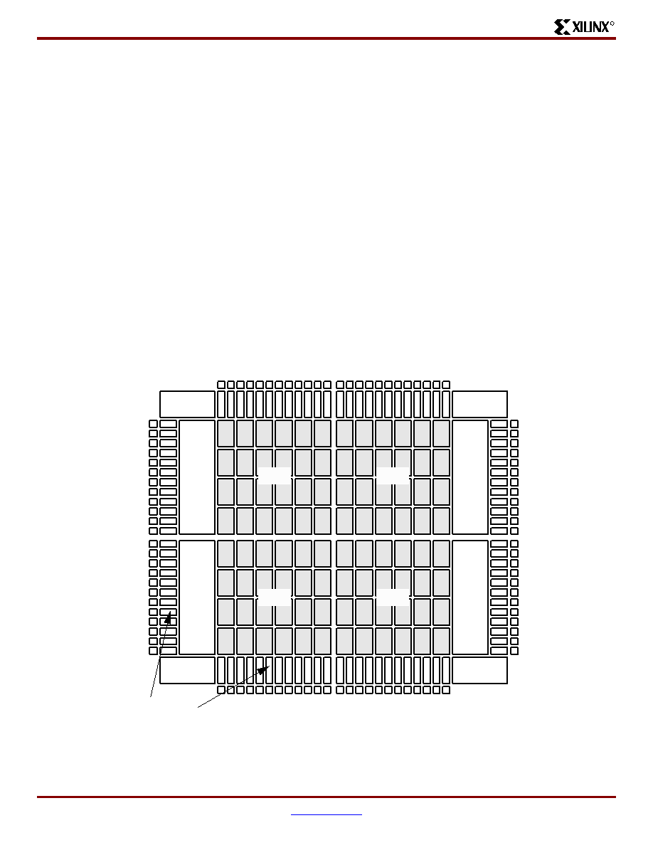
General Overview
The Spartan-II family of FPGAs have a regular, flexible, pro-
grammable architecture of Configurable Logic Blocks
(CLBs), surrounded by a perimeter of programmable
Input/Output Blocks (IOBs). There are four Delay-Locked
Loops (DLLs), one at each corner of the die. Two columns
of block RAM lie on opposite sides of the die, between the
CLBs and the IOB columns. These functional elements are
interconnected by a powerful hierarchy of versatile routing
channels (see
Figure 1
).
Spartan-II FPGAs are customized by loading configuration
data into internal static memory cells. Unlimited reprogram-
ming cycles are possible with this approach. Stored values
in these cells determine logic functions and interconnec-
tions implemented in the FPGA. Configuration data can be
read from an external serial PROM (master serial mode), or
written into the FPGA in slave serial, slave parallel, or
Boundary Scan modes.
Spartan-II FPGAs are typically used in high-volume applica-
tions where the versatility of a fast programmable solution
adds benefits. Spartan-II FPGAs are ideal for shortening
product development cycles while offering a cost-effective
solution for high volume production.
Spartan-II FPGAs achieve high-performance, low-cost
operation through advanced architecture and semiconduc-
tor technology. Spartan-II devices provide system clock
rates up to 200 MHz. Spartan-II FPGAs offer the most
cost-effective solution while maintaining leading edge per-
formance. In addition to the conventional benefits of
high-volume programmable logic solutions, Spartan-II
FPGAs also offer on-chip synchronous single-port and
dual-port RAM (block and distributed form), DLL clock driv-
ers, programmable set and reset on all flip-flops, fast carry
logic, and many other features.
The Xilinx XC17S00A PROM family is recommended for
serial configuration of Spartan-II FPGAs. The In-System
Programmable (ISP) XC18V00 PROM family is recom-
mended for parallel or serial configuration.
Figure 1: Basic Spartan-II Family FPGA Block Diagram
XC2S15
DLL
DLL
DLL
DLL
BLOCK RAM
BLOCK RAM
BLOCK RAM
BLOCK RAM
I/O LOGIC
CLBs
CLBs
CLBs
CLBs
DS001_01_091800

Spartan-II 2.5V FPGA Family: Introduction and Ordering Information
DS001-1 (v2.4) September 3, 2003
www.xilinx.com
3
Product Specification
1-800-255-7778
R
Spartan-II Product Availability
Table 2
shows the package and speed grades available for
Spartan-II family devices.
Table 3
shows the maximum user
I/Os available on the device and the number of user I/Os
available for each device/package combination. The four
global clock pins are usable as additional user I/Os when
not used as a global clock pin. These pins are not included
in user I/O counts.
Table 2: Spartan-II Package and Speed Grade Availability
Device
Pins
100
144
144
208
256
456
Type
Plastic
VQFP
Plastic
TQFP
Chip Scale
BGA
Plastic
PQFP
Fine Pitch
BGA
Fine Pitch
BGA
Code
VQ100
TQ144
CS144
PQ208
FG256
FG456
XC2S15
-5
C, I
C, I
C, I
-
-
-
-6
C
C
C
-
-
-
XC2S30
-5
C, I
C, I
C, I
C, I
-
-
-6
C
C
C
C
-
-
XC2S50
-5
-
C, I
-
C, I
C, I
-
-6
-
C
-
C
C
-
XC2S100
-5
-
C, I
-
C, I
C, I
C, I
-6
-
C
-
C
C
C
XC2S150
-5
-
-
-
C, I
C, I
C, I
-6
-
-
-
C
C
C
XC2S200
-5
-
-
-
C, I
C, I
C, I
-6
-
-
-
C
C
C
Notes:
1.
C = Commercial, T
J
= 0
∞ to +85∞ C; I = Industrial, T
J
= ≠40
∞ C to +100∞ C.
Table 3: Spartan-II User I/O Chart
(1)
Device
Maximum
User I/O
Available User I/O According to Package Type
VQ100
TQ144
CS144
PQ208
FG256
FG456
XC2S15
86
60
86
86
-
-
-
XC2S30
132
60
92
92
132
-
-
XC2S50
176
-
92
-
140
176
-
XC2S100
196
-
92
-
140
176
196
XC2S150
260
-
-
-
140
176
260
XC2S200
284
-
-
-
140
176
284
Notes:
1.
All user I/O counts do not include the four global clock/user input pins.

Spartan-II 2.5V FPGA Family: Introduction and Ordering Information
4
www.xilinx.com
DS001-1 (v2.4) September 3, 2003
1-800-255-7778
Product Specification
R
Ordering Information
Device Part Marking
Revision History
XC2S50 -6 PQ 208 C
Example:
Temperature Range
Number of Pins
Package Type
Device Type
Speed Grade
Device Ordering Options
Device
Speed Grade
Number of Pins / Package Type
Temperature Range (T
J
)
XC2S15
-5
Standard Performance
VQ100
100-pin Plastic Very Thin QFP
C = Commercial
0∞C to +85∞C
XC2S30
-6
Higher Performance
CS144
144-ball Chip-Scale BGA
I = Industrial
≠40∞C to +100∞C
XC2S50
TQ144
144-pin Plastic Thin QFP
XC2S100
PQ208
208-pin Plastic QFP
XC2S150
FG256
256-ball Fine Pitch BGA
XC2S200
FG456
456-ball Fine Pitch BGA
Date
Version No.
Description
09/18/00
2.0
Sectioned the Spartan-II Family data sheet into four modules. Added industrial temperature
range information.
10/31/00
2.1
Removed Power down feature.
03/05/01
2.2
Added statement on PROMs.
11/01/01
2.3
Updated Product Availability chart. Minor text edits.
09/03/03
2.4
Added device part marking.
Lot Code
Date Code
Sample package with part marking
for XC2S50-6PQ208C.
XC2S50
TM
PQ208AFP0025
A1134280A
6C
SPARTAN
Device Type
Package
Speed
Operating Range
R
R
ds001-1_02_090303