DS031 October 14, 2003
www.xilinx.com
Product Specification
1-800-255-7778
© 2003 Xilinx, Inc. All rights reserved. All Xilinx trademarks, registered trademarks, patents, and disclaimers are as listed at
http://www.xilinx.com/legal.htm
.
All other trademarks and registered trademarks are the property of their respective owners. All specifications are subject to change without notice.
This document includes all four modules of the Virtex-II Platform FPGA data sheet.
Module 1:
Introduction and Overview
DS031-1 (v2.0) August 1, 2003
7 pages
∑
Summary of Features
∑
General Description
∑
Device/Package Combinations and Maximum I/O
∑
Ordering Information
Module 2:
Functional Description
DS031-2 (v3.1) October 14, 2003
40 pages
∑
Detailed Description
∑
Digitally Controlled Impedance (DCI)
∑
Configurable Logic Blocks (CLBs)
∑
Sum of Products
∑
3-State Buffers
∑
18-Kb Block SelectRAMTM Resources
∑
18-Bit x 18-Bit Multipliers
∑
Global Clock Multiplexer Buffers
∑
Digital Clock Manager (DCM)
∑
Active Interconnect Technology
∑
Creating a Design
∑
Configuration
Module 3:
DC and Switching Characteristics
DS031-3 (v3.1) October 14, 2003
38 pages
∑
Electrical Characteristics
∑
Performance Characteristics
∑
Switching Characteristics
∑
Pin-to-Pin Output Parameter Guidelines
∑
Pin-to-Pin Input Parameter Guidelines
∑
DCM Timing Parameters
Module 4:
Pinout Information
DS031-4 (v2.0) August 1, 2003
225 pages
∑
Pin Definitions
∑
Pinout Tables
-
CS144 Chip-Scale BGA Package
-
FG256 Fine-Pitch BGA Package
-
FG456 Fine-Pitch BGA Package
-
FG676 Fine-Pitch BGA Package
-
BG575 Standard BGA Package
-
BG728 Standard BGA Package
-
FF896 Flip-Chip Fine-Pitch BGA Package
-
FF1152 Flip-Chip Fine-Pitch BGA Package
-
FF1517 Flip-Chip Fine-Pitch BGA Package
-
BF957Flip-Chip BGA Package
IMPORTANT NOTE: The Virtex-II Platform FPGA data sheet is created and published in separate modules. This complete
version is provided for easy downloading and searching of the complete document. Page, figure, and table numbers begin
at 1 for each module, and each module has its own Revision History at the end. Use the PDF "Bookmarks" pane for easy
navigation in this volume.
0
VirtexTM-II Platform FPGAs:
Complete Data Sheet
DS031 October 14, 2003
0
0
Product Specification
R
© 2001-2002 Xilinx, Inc. All rights reserved. All Xilinx trademarks, registered trademarks, patents, and disclaimers are as listed at
http://www.xilinx.com/legal.htm
.
All other trademarks and registered trademarks are the property of their respective owners. All specifications are subject to change without notice.
DS031-1 (v2.0) August 1, 2003
www.xilinx.com
Module 1 of 4
Product Specification
1-800-255-7778
1
Summary of Virtex-II Features
∑
Industry First Platform FPGA Solution
∑
IP-Immersion Architecture
-
Densities from 40K to 8M system gates
-
420 MHz internal clock speed (Advance Data)
-
840+ Mb/s I/O (Advance Data)
∑
SelectRAMTM Memory Hierarchy
-
3 Mb of dual-port RAM in 18 Kbit block SelectRAM
resources
-
Up to 1.5 Mb of distributed SelectRAM resources
∑
High-Performance Interfaces to External Memory
-
DRAM interfaces
∑
SDR / DDR SDRAM
∑
Network FCRAM
∑
Reduced Latency DRAM
-
SRAM interfaces
∑
SDR / DDR SRAM
∑
QDRTM SRAM
-
CAM interfaces
∑
Arithmetic Functions
-
Dedicated 18-bit x 18-bit multiplier blocks
-
Fast look-ahead carry logic chains
∑
Flexible Logic Resources
-
Up to 93,184 internal registers / latches with Clock
Enable
-
Up to 93,184 look-up tables (LUTs) or cascadable
16-bit shift registers
-
Wide multiplexers and wide-input function support
-
Horizontal cascade chain and sum-of-products
support
-
Internal 3-state bussing
∑
High-Performance Clock Management Circuitry
-
Up to 12 DCM (Digital Clock Manager) modules
∑
Precise clock de-skew
∑
Flexible frequency synthesis
∑
High-resolution phase shifting
-
16 global clock multiplexer buffers
∑
Active Interconnect Technology
-
Fourth generation segmented routing structure
-
Predictable, fast routing delay, independent of fanout
∑
SelectIOTM-Ultra Technology
-
Up to 1,108 user I/Os
-
19 single-ended and six differential standards
-
Programmable sink current (2 mA to 24 mA) per I/O
-
Digitally Controlled Impedance (DCI) I/O: on-chip
termination resistors for single-ended I/O standards
-
PCI-X compatible (133 MHz and 66 MHz) at 3.3V
-
PCI compliant (66 MHz and 33 MHz) at 3.3V
-
CardBus compliant (33 MHz) at 3.3V
-
Differential Signaling
∑
840 Mb/s Low-Voltage Differential Signaling I/O
(LVDS) with current mode drivers
∑
Bus LVDS I/O
∑
Lightning Data Transport (LDT) I/O with current
driver buffers
∑
Low-Voltage Positive Emitter-Coupled Logic
(LVPECL) I/O
∑
Built-in DDR input and output registers
-
Proprietary high-performance SelectLink
Technology
∑
High-bandwidth data path
∑
Double Data Rate (DDR) link
∑
Web-based HDL generation methodology
∑
Supported by Xilinx FoundationTM and Alliance
SeriesTM Development Systems
-
Integrated VHDL and Verilog design flows
-
Compilation of 10M system gates designs
-
Internet Team Design (ITD) tool
∑
SRAM-Based In-System Configuration
-
Fast SelectMAP configuration
-
Triple Data Encryption Standard (DES) security
option (Bitstream Encryption)
-
IEEE 1532 support
-
Partial reconfiguration
-
Unlimited reprogrammability
-
Readback capability
∑
0.15 µm 8-Layer Metal Process with 0.12 µm
High-Speed Transistors
∑
1.5V (V
CCINT
) Core Power Supply, Dedicated 3.3V
V
CCAUX
Auxiliary and V
CCO
I/O Power Supplies
∑
IEEE 1149.1 Compatible Boundary-Scan Logic
Support
∑
Flip-Chip and Wire-Bond Ball Grid Array (BGA)
Packages in Three Standard Fine Pitches (0.80 mm,
1.00 mm, and 1.27 mm)
∑
100% Factory Tested
0
7
VirtexTM-II Platform FPGAs:
Introduction and Overview
DS031-1 (v2.0) August 1, 2003
0
0
Product Specification
R

VirtexTM-II Platform FPGAs: Introduction and Overview
R
DS031-1 (v2.0) August 1, 2003
www.xilinx.com
Module 1 of 4
Product Specification
1-800-255-7778
2
General Description
The Virtex-II family is a platform FPGA developed for high
performance from low-density to high-density designs that
are based on IP cores and customized modules. The family
delivers complete solutions for telecommunication, wire-
less, networking, video, and DSP applications, including
PCI, LVDS, and DDR interfaces.
The leading-edge 0.15 µm / 0.12 µm CMOS 8-layer metal
process and the Virtex-II architecture are optimized for high
speed with low power consumption. Combining a wide vari-
ety of flexible features and a large range of densities up to
10 million system gates, the Virtex-II family enhances pro-
grammable logic design capabilities and is a powerful alter-
native to mask-programmed gates arrays. As shown in
Table 1
, the Virtex-II family comprises 11 members, ranging
from 40K to 8M system gates.
Packaging
Offerings include ball grid array (BGA) packages with
0.80 mm, 1.00 mm, and 1.27 mm pitches. In addition to tra-
ditional wire-bond interconnects, flip-chip interconnect is
used in some of the BGA offerings. The use of flip-chip
interconnect offers more I/Os than is possible in wire-bond
versions of the similar packages. Flip-chip construction
offers the combination of high pin count with high thermal
capacity.
Table 2
shows the maximum number of user I/Os available.
The Virtex-II device/package combination table (
Table 6
at
the end of this section) details the maximum number of I/Os
for each device and package using wire-bond or flip-chip
technology.
Table 1: Virtex-II Field-Programmable Gate Array Family Members
Device
System
Gates
CLB
(1 CLB = 4 slices = Max 128 bits)
Multiplier
Blocks
SelectRAM Blocks
DCMs
Max I/O
Pads
(1)
Array
Row x Col.
Slices
Maximum
Distributed
RAM Kbits
18 Kbit
Blocks
Max RAM
(Kbits)
XC2V40
40K
8 x 8
256
8
4
4
72
4
88
XC2V80
80K
16 x 8
512
16
8
8
144
4
120
XC2V250
250K
24 x 16
1,536
48
24
24
432
8
200
XC2V500
500K
32 x 24
3,072
96
32
32
576
8
264
XC2V1000
1M
40 x 32
5,120
160
40
40
720
8
432
XC2V1500
1.5M
48 x 40
7,680
240
48
48
864
8
528
XC2V2000
2M
56 x 48
10,752
336
56
56
1,008
8
624
XC2V3000
3M
64 x 56
14,336
448
96
96
1,728
12
720
XC2V4000
4M
80 x 72
23,040
720
120
120
2,160
12
912
XC2V6000
6M
96 x 88
33,792
1,056
144
144
2,592
12
1,104
XC2V8000
8M
112 x 104
46,592
1,456
168
168
3,024
12
1,108
Notes:
1.
See details in
Table 2, "Maximum Number of User I/O Pads"
.
Table 2: Maximum Number of User I/O Pads
Device
Wire-Bond
Flip-Chip
XC2V40
88
-
XC2V80
120
-
XC2V250
200
-
XC2V500
264
-
XC2V1000
328
432
XC2V1500
392
528
XC2V2000
-
624
XC2V3000
516
720
XC2V4000
-
912
XC2V6000
-
1,104
XC2V8000
-
1,108

VirtexTM-II Platform FPGAs: Introduction and Overview
R
DS031-1 (v2.0) August 1, 2003
www.xilinx.com
Module 1 of 4
Product Specification
1-800-255-7778
3
Architecture
Virtex-II Array Overview
Virtex-II devices are user-programmable gate arrays with
various configurable elements. The Virtex-II architecture is
optimized for high-density and high-performance logic
designs. As shown in
Figure 1
, the programmable device is
comprised of input/output blocks (IOBs) and internal
configurable logic blocks (CLBs).
Programmable I/O blocks provide the interface between
package pins and the internal configurable logic. Most
popular and leading-edge I/O standards are supported by
the programmable IOBs.
The internal configurable logic includes four major elements
organized in a regular array.
∑
Configurable Logic Blocks (CLBs) provide functional
elements for combinatorial and synchronous logic,
including basic storage elements. BUFTs (3-state
buffers) associated with each CLB element drive
dedicated segmentable horizontal routing resources.
∑
Block SelectRAM memory modules provide large
18 Kbit storage elements of dual-port RAM.
∑
Multiplier blocks are 18-bit x 18-bit dedicated
multipliers.
∑
DCM (Digital Clock Manager) blocks provide
self-calibrating, fully digital solutions for clock
distribution delay compensation, clock multiplication
and division, coarse- and fine-grained clock phase
shifting.
A new generation of programmable routing resources called
Active Interconnect Technology interconnects all of these
elements. The general routing matrix (GRM) is an array of
routing switches. Each programmable element is tied to a
switch matrix, allowing multiple connections to the general
routing matrix. The overall programmable interconnection is
hierarchical and designed to support high-speed designs.
All programmable elements, including the routing
resources, are controlled by values stored in static memory
cells. These values are loaded in the memory cells during
configuration and can be reloaded to change the functions
of the programmable elements.
Virtex-II Features
This section briefly describes Virtex-II features.
Input/Output Blocks (IOBs)
IOBs are programmable and can be categorized as follows:
∑
Input block with an optional single-data-rate or
double-data-rate (DDR) register
∑
Output block with an optional single-data-rate or DDR
register, and an optional 3-state buffer, to be driven
directly or through a single or DDR register
∑
Bidirectional block (any combination of input and output
configurations)
These registers are either edge-triggered D-type flip-flops
or level-sensitive latches.
IOBs support the following single-ended I/O standards:
∑
LVTTL, LVCMOS (3.3V, 2.5V, 1.8V, and 1.5V)
∑
PCI-X compatible (133 MHz and 66 MHz) at 3.3V
∑
PCI compliant (66 MHz and 33 MHz) at 3.3V
∑
CardBus compliant (33 MHz) at 3.3V
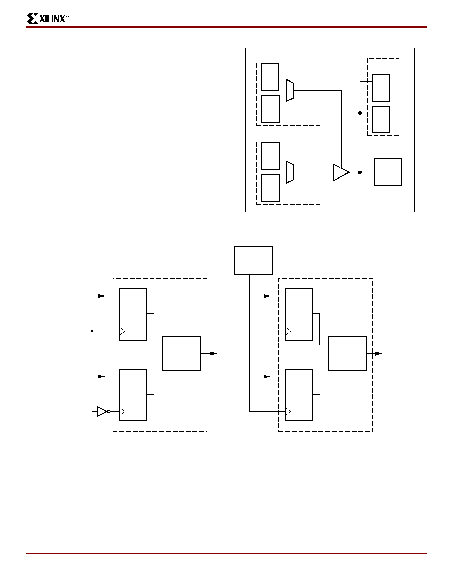
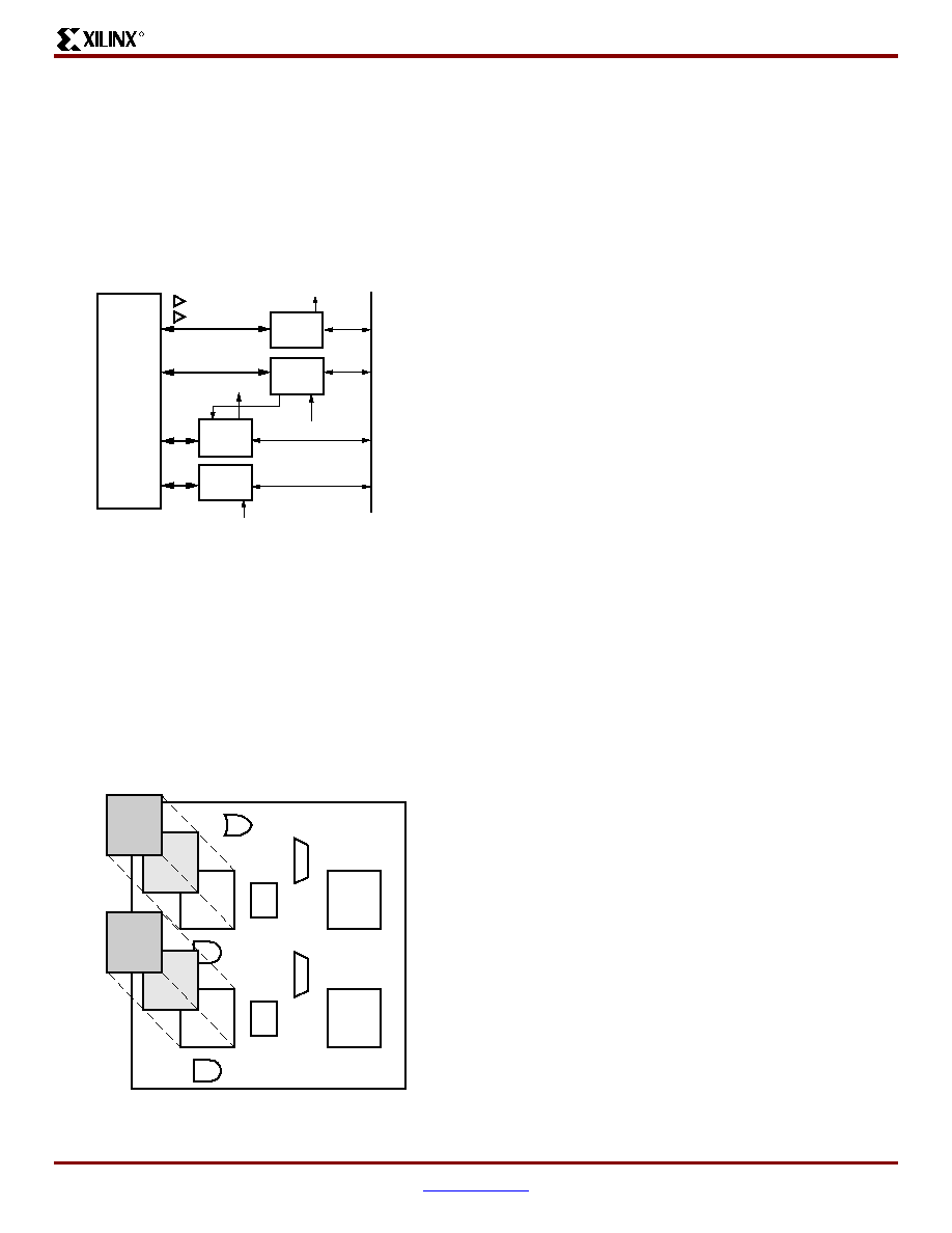
Figure 1: Virtex-II Architecture Overview
Global Clock Mux
DCM
DCM
IOB
CLB
Programmable I/Os
Block SelectRAM
Multiplier
Configurable Logic
DS031_28_100900
VirtexTM-II Platform FPGAs: Introduction and Overview
R
DS031-1 (v2.0) August 1, 2003
www.xilinx.com
Module 1 of 4
Product Specification
1-800-255-7778
4
∑
GTL and GTLP
∑
HSTL (Class I, II, III, and IV)
∑
SSTL (3.3V and 2.5V, Class I and II)
∑
AGP-2X
The digitally controlled impedance (DCI) I/O feature auto-
matically provides on-chip termination for each I/O element.
The IOB elements also support the following differential sig-
naling I/O standards:
∑
LVDS
∑
BLVDS (Bus LVDS)
∑
ULVDS
∑
LDT
∑
LVPECL
Two adjacent pads are used for each differential pair. Two or
four IOB blocks connect to one switch matrix to access the
routing resources.
Configurable Logic Blocks (CLBs)
CLB resources include four slices and two 3-state buffers.
Each slice is equivalent and contains:
∑
Two function generators (F & G)
∑
Two storage elements
∑
Arithmetic logic gates
∑
Large multiplexers
∑
Wide function capability
∑
Fast carry look-ahead chain
∑
Horizontal cascade chain (OR gate)
The function generators F & G are configurable as 4-input
look-up tables (LUTs), as 16-bit shift registers, or as 16-bit
distributed SelectRAM memory.
In addition, the two storage elements are either edge-trig-
gered D-type flip-flops or level-sensitive latches.
Each CLB has internal fast interconnect and connects to a
switch matrix to access general routing resources.
Block SelectRAM Memory
The block SelectRAM memory resources are 18 Kb of
dual-port RAM, programmable from 16K x 1 bit to 512 x 36
bits, in various depth and width configurations. Each port is
totally synchronous and independent, offering three
"read-during-write" modes. Block SelectRAM memory is
cascadable to implement large embedded storage blocks.
Supported memory configurations for dual-port and sin-
gle-port modes are shown in
Table 3
.
A multiplier block is associated with each SelectRAM mem-
ory block. The multiplier block is a dedicated 18 x 18-bit
multiplier and is optimized for operations based on the block
SelectRAM content on one port. The 18 x 18 multiplier can
be used independently of the block SelectRAM resource.
Read/multiply/accumulate operations and DSP filter struc-
tures are extremely efficient.
Both the SelectRAM memory and the multiplier resource
are connected to four switch matrices to access the general
routing resources.
Global Clocking
The DCM and global clock multiplexer buffers provide a
complete solution for designing high-speed clocking
schemes.
Up to 12 DCM blocks are available. To generate de-skewed
internal or external clocks, each DCM can be used to elimi-
nate clock distribution delay. The DCM also provides 90-,
180-, and 270-degree phase-shifted versions of its output
clocks. Fine-grained phase shifting offers high-resolution
phase adjustments in increments of 1/256 of the clock
period. Very flexible frequency synthesis provides a clock
output frequency equal to any M/D ratio of the input clock
frequency, where M and D are two integers. For the exact
timing parameters, see
Virtex-II Electrical Characteris-
tics
.
Virtex-II devices have 16 global clock MUX buffers, with up
to eight clock nets per quadrant. Each global clock MUX
buffer can select one of the two clock inputs and switch
glitch-free from one clock to the other. Each DCM block is
able to drive up to four of the 16 global clock MUX buffers.
Routing Resources
The IOB, CLB, block SelectRAM, multiplier, and DCM ele-
ments all use the same interconnect scheme and the same
access to the global routing matrix. Timing models are
shared, greatly improving the predictability of the perfor-
mance of high-speed designs.
There are a total of 16 global clock lines, with eight available
per quadrant. In addition, 24 vertical and horizontal long
lines per row or column as well as massive secondary and
local routing resources provide fast interconnect. Virtex-II
buffered interconnects are relatively unaffected by net
fanout and the interconnect layout is designed to minimize
crosstalk.
Horizontal and vertical routing resources for each row or
column include:
∑
24 long lines
∑
120 hex lines
∑
40 double lines
∑
16 direct connect lines (total in all four directions)
Table 3: Dual-Port And Single-Port Configurations
16K x 1 bit
2K x 9 bits
8K x 2 bits
1K x 18 bits
4K x 4 bits
512 x 36 bits

VirtexTM-II Platform FPGAs: Introduction and Overview
R
DS031-1 (v2.0) August 1, 2003
www.xilinx.com
Module 1 of 4
Product Specification
1-800-255-7778
5
Boundary Scan
Boundary scan instructions and associated data registers
support a standard methodology for accessing and config-
uring Virtex-II devices that complies with IEEE standards
1149.1 -- 1993 and 1532. A system mode and a test mode
are implemented. In system mode, a Virtex-II device per-
forms its intended mission even while executing non-test
boundary-scan instructions. In test mode, boundary-scan
test instructions control the I/O pins for testing purposes.
The Virtex-II Test Access Port (TAP) supports BYPASS,
PRELOAD, SAMPLE, IDCODE, and USERCODE non-test
instructions. The EXTEST, INTEST, and HIGHZ test instruc-
tions are also supported.
Configuration
Virtex-II devices are configured by loading data into internal
configuration memory, using the following five modes:
∑
Slave-serial mode
∑
Master-serial mode
∑
Slave SelectMAP mode
∑
Master SelectMAP mode
∑
Boundary-Scan mode (IEEE 1532)
A Data Encryption Standard (DES) decryptor is available
on-chip to secure the bitstreams. One or two triple-DES key
sets can be used to optionally encrypt the configuration
information.
Readback and Integrated Logic Analyzer
Configuration data stored in Virtex-II configuration memory
can be read back for verification. Along with the configura-
tion data, the contents of all flip-flops/latches, distributed
SelectRAM, and block SelectRAM memory resources can
be read back. This capability is useful for real-time debug-
ging.
The Integrated Logic Analyzer (ILA) core and software pro-
vides a complete solution for accessing and verifying
Virtex-II devices.
Virtex-II Device/Package Combinations
and Maximum I/O
Wire-bond and flip-chip packages are available.
Table 4
and
Table 5
show the maximum possible number of user I/Os in
wire-bond and flip-chip packages, respectively.
Table 6
shows the number of available user I/Os for all device/pack-
age combinations.
∑
CS denotes wire-bond chip-scale ball grid array (BGA)
(0.80 mm pitch).
∑
FG denotes wire-bond fine-pitch BGA (1.00 mm pitch).
∑
FF denotes flip-chip fine-pitch BGA (1.00 mm pitch).
∑
BG denotes standard BGA (1.27 mm pitch).
∑
BF denotes flip-chip BGA (1.27 mm pitch).
The number of I/Os per package include all user I/Os except
the 15 control pins (CCLK, DONE, M0, M1, M2, PROG_B,
PWRDWN_B, TCK, TDI, TDO, TMS, HSWAP_EN, DXN,
DXP, and RSVD) and VBATT.
Table 4: Wire-Bond Packages Information
Package
CS144
FG256
FG456
FG676
BG575
BG728
Pitch (mm)
0.80
1.00
1.00
1.00
1.27
1.27
Size (mm)
12 x 12
17 x 17
23 x 23
27 x 27
31 x 31
35 x 35
I/Os
92
172
324
484
408
516
Table 5: Flip-Chip Packages Information
Package
FF896
FF1152
FF1517
BF957
Pitch (mm)
1.00
1.00
1.00
1.27
Size (mm)
31 x 31
35 x 35
40 x 40
40 x 40
I/Os
624
824
1,108
684

VirtexTM-II Platform FPGAs: Introduction and Overview
R
DS031-1 (v2.0) August 1, 2003
www.xilinx.com
Module 1 of 4
Product Specification
1-800-255-7778
6
Virtex-II Ordering Information
Table 6: Virtex-II Device/Package Combinations and Maximum Number of Available I/Os (Advance Information)
Package
Available I/Os
XC2V
40
XC2V
80
XC2V
250
XC2V
500
XC2V
1000
XC2V
1500
XC2V
2000
XC2V
3000
XC2V
4000
XC2V
6000
XC2V
8000
CS144
88
92
92
-
-
-
-
-
-
-
-
FG256
88
120
172
172
172
-
-
-
-
-
-
FG456
-
-
200
264
324
-
-
-
-
-
-
FG676
-
-
-
-
-
392
456
484
-
-
-
FF896
-
-
-
-
432
528
624
-
-
-
-
FF1152
-
-
-
-
-
-
-
720
824
824
824
FF1517
-
-
-
-
-
-
-
-
912
1,104
1,108
BG575
-
-
-
-
328
392
408
-
-
-
-
BG728
-
-
-
-
-
-
-
516
-
-
-
BF957
-
-
-
-
-
-
624
684
684
684
-
Notes:
1.
All devices in a particular package are pinout (footprint) compatible. In addition, the FG456 and FG676 packages are compatible, as
are the FF896 and FF1152 packages.
Figure 2: Virtex-II Ordering Information
Example: XC2V1000-5FG456C
Device Type
Temperature Range
C = Commercial (Tj = 0∞C to +85∞C)
I = Industrial (Tj = ≠40∞C to +100∞C)
Number of Pins
Package Type
Speed Grade
(-4, -5, -6)
DS031_35_033001

VirtexTM-II Platform FPGAs: Introduction and Overview
R
DS031-1 (v2.0) August 1, 2003
www.xilinx.com
Module 1 of 4
Product Specification
1-800-255-7778
7
Revision History
This section records the change history for this module of the data sheet.
Virtex-II Data Sheet
The Virtex-II Data Sheet contains the following modules:
∑
VirtexTM-II Platform FPGAs: Introduction and Overview
(Module 1)
∑
VirtexTM-II Platform FPGAs: Detailed Description
(Module 2)
∑
VirtexTM-II Platform FPGAs: DC and Switching
Characteristics (Module 3)
∑
VirtexTM-II Platform FPGAs: Pinout Information
(Module 4)
Date
Version
Revision
11/07/00
1.0
Early access draft.
12/06/00
1.1
Initial release.
01/15/01
1.2
Added values to the tables in the
Virtex-II Performance Characteristics
and
Virtex-II
Switching Characteristics
sections.
01/25/01
1.3
The data sheet was divided into four modules (per the current style standard).
04/02/01
1.5
Skipped v1.4 to sync up modules. Reverted to traditional double-column format.
07/30/01
1.6
Made minor changes to items listed under
Summary of Virtex-II Features
.
10/02/01
1.7
Minor edits.
07/16/02
1.8
Updated Virtex-II Device/Package Combinations shown in
Table 6
.
09/26/02
1.9
Updated
Table 2
and
Table 6
to reflect supported Virtex-II Device/Package Combinations.
08/01/03
2.0
All Virtex-II devices and speed grades now Production. See Table 13, Module 3.
© 2001-2002 Xilinx, Inc. All rights reserved. All Xilinx trademarks, registered trademarks, patents, and disclaimers are as listed at
http://www.xilinx.com/legal.htm
.
All other trademarks and registered trademarks are the property of their respective owners. All specifications are subject to change without notice.
DS031-2 (v3.1) October 14, 2003
www.xilinx.com
Module 2 of 4
Product Specification
1-800-255-7778
1
Detailed Description
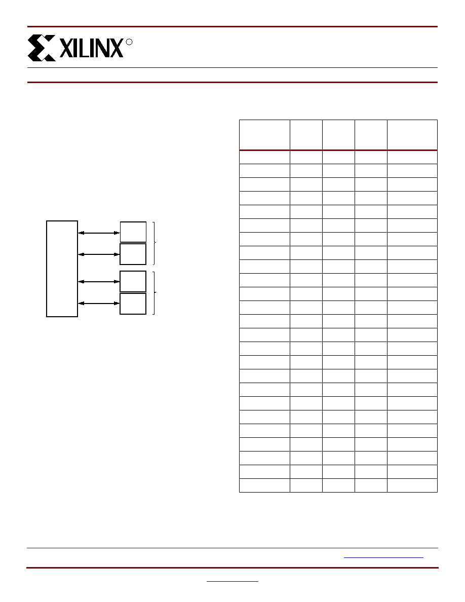
Input/Output Blocks (IOBs)
Virtex-II I/O blocks (IOBs) are provided in groups of two or
four on the perimeter of each device. Each IOB can be used
as input and/or output for single-ended I/Os. Two IOBs can
be used as a differential pair. A differential pair is always
connected to the same switch matrix, as shown in
Figure 1
.
IOB blocks are designed for high performances I/Os, sup-
porting 19 single-ended standards, as well as differential
signaling with LVDS, LDT, Bus LVDS, and LVPECL.
Note: Differential I/Os must use the same clock.
Supported I/O Standards
Virtex-II IOB blocks feature SelectI/O-Ultra inputs and out-
puts that support a wide variety of I/O signaling standards.
In addition to the internal supply voltage (V
CCINT
= 1.5V),
output driver supply voltage (V
CCO
) is dependent on the I/O
standard (see
Table 1
). An auxiliary supply voltage
(V
CCAUX
= 3.3 V) is required, regardless of the I/O stan-
dard used. For exact supply voltage absolute maximum rat-
ings, see
DC Input and Output Levels
in Module 3.
0
40
VirtexTM-II Platform FPGAs:
Detailed Description
DS031-2 (v3.1) October 14, 2003
0
0
Product Specification
R
Figure 1: Virtex-II Input/Output Tile
IOB
PAD4
IOB
PAD3
Differential Pair
IOB
PAD2
IOB
PAD1
Differential Pair
Switch
Matrix
DS031_30_101600
Table 1: Supported Single-Ended I/O Standards
I/O
Standard
Output
V
CCO
Input
V
CCO
Input
V
REF
Board
Termination
Voltage (V
TT
)
LVTTL
3.3
3.3
N/R
(3)
N/R
LVCMOS33
3.3
3.3
N/R
N/R
LVCMOS25
2.5
2.5
N/R
N/R
LVCMOS18
1.8
1.8
N/R
N/R
LVCMOS15
1.5
1.5
N/R
N/R
PCI33_3 3.3
3.3
N/R
N/R
PCI66_3 3.3
3.3
N/R
N/R
PCI-X
3.3
3.3
N/R
N/R
GTL
Note (1)
Note (1)
0.8
1.2
GTLP
Note (1)
Note (1)
1.0
1.5
HSTL_I
1.5 N/R
0.75
0.75
HSTL_II
1.5
N/R
0.75
0.75
HSTL_III 1.5
N/R
0.9
1.5
HSTL_IV
1.5 N/R
0.9
1.5
HSTL_I_18
1.8 N/R
0.9
0.9
HSTL_II_18
1.8 N/R
0.9
0.9
HSTL_III _18
1.8
N/R
1.1
1.8
HSTL_IV_18
1.8 N/R
1.1
1.8
SSTL18_I
(2)
1.8
N/R
0.9
0.9
SSTL18_II
1.8
N/R
0.9
0.9
SSTL2_I 2.5
N/R
1.25
1.25
SSTL2_II
2.5
N/R
1.25
1.25
SSTL3_I 3.3
N/R
1.5
1.5
SSTL3_II
3.3
N/R
1.5
1.5
AGP-2X/AGP
3.3
N/R
1.32
N/R
Notes:
1.
V
CCO
of GTL or GTLP should not be lower than the
termination voltage or the voltage seen at the I/O pad.
2.
SSTL18_I is not a JEDEC-supported standard.
3.
N/R = no requirement.

VirtexTM-II Platform FPGAs: Detailed Description
R
DS031-2 (v3.1) October 14, 2003
www.xilinx.com
Module 2 of 4
Product Specification
1-800-255-7778
2
All of the user IOBs have fixed-clamp diodes to VCCO and
to ground. As outputs, these IOBs are not compatible or
compliant with 5V I/O standards. As inputs, these IOBs are
not normally 5V tolerant, but can be used with 5V I/O stan-
dards when external current-limiting resistors are used. For
more details, see the "5V Tolerant I/Os" Tech Topic at
www.xilinx.com
.
Table 3
lists supported I/O standards with Digitally Con-
trolled Impedance. See
Digitally Controlled Impedance
(DCI), page 8
.
Table 2: Supported Differential Signal I/O Standards
I/O Standard
Output
V
CCO
Input
V
CCO
Input
V
REF
Output
V
OD
LVPECL_33
3.3
N/R
(1)
N/R
490 mV to 1.22V
LDT_25
2.5
N/R
N/R
0.430 - 0.670
LVDS_33
3.3
N/R
N/R
0.250 - 0.400
LVDS_25
2.5
N/R
N/R
0.250 - 0.400
LVDSEXT_33
3.3
N/R
N/R
0.330 - 0.700
LVDSEXT_25
2.5
N/R
N/R
0.330 - 0.700
BLVDS_25
2.5
N/R
N/R
0.250 - 0.450
ULVDS_25
2.5
N/R
N/R
0.430 - 0.670
Notes:
1.
N/R = no requirement.
Table 3: Supported DCI I/O Standards
I/O
Standard
Output
V
CCO
Input
V
CCO
Input
V
REF
Termination
Type
LVDCI_33
(1)
3.3
3.3
N/R
(4)
Series
LVDCI_DV2_33
(1)
3.3
3.3
N/R
Series
LVDCI_25
(1)
2.5
2.5
N/R
Series
LVDCI_DV2_25
(1)
2.5
2.5
N/R
Series
LVDCI_18
(1)
1.8
1.8
N/R
Series
LVDCI_DV2_18
(1)
1.8
1.8
N/R
Series
LVDCI_15
(1)
1.5
1.5
N/R
Series
LVDCI_DV2_15
(1)
1.5
1.5
N/R
Series
GTL_DCI
1.2
1.2
0.8
Single
GTLP_DCI
1.5
1.5
1.0
Single
HSTL_I_DCI
1.5
1.5
0.75
Split
HSTL_II_DCI
1.5
1.5
0.75
Split
HSTL_III_DCI
1.5
1.5
0.9
Single
HSTL_IV_DCI
1.5
1.5
0.9
Single
HSTL_I_DCI_18
1.8
1.8
0.9
Split
HSTL_II_DCI_18
1.8
1.8
0.9
Split
HSTL_III_DCI_18
1.8
1.8
1.1
Single
HSTL_IV_DCI_18
1.8
1.8
1.1
Single
SSTL18_I_DCI
(3)
1.8
1.8
0.9
Split
SSTL18_II_DCI
1.8
1.8
0.9
Split
SSTL2_I_DCI
(2)
2.5
2.5
1.25
Split
SSTL2_II_DCI
(2)
2.5
2.5
1.25
Split
SSTL3_I_DCI
(2)
3.3
3.3
1.5
Split
SSTL3_II_DCI
(2)
3.3
3.3
1.5
Split
LVDS_33_DCI
3.3
3.3
N/R
Split
LVDS_25_DCI
2.5
2.5
N/R
Split
LVDSEXT_33_DCI
3.3
3.3
N/R
Split
LVDSEXT_25_DCI
2.5
2.5
N/R
Split
Notes:
1.
LVDCI_XX and LVDCI_DV2_XX are LVCMOS controlled
impedance buffers, matching the reference resistors or half
of the reference resistors.
2.
These are SSTL compatible.
3.
SSTL18_I is not a JEDEC-supported standard.
4.
N/R = no requirement.
VirtexTM-II Platform FPGAs: Detailed Description
R
DS031-2 (v3.1) October 14, 2003
www.xilinx.com
Module 2 of 4
Product Specification
1-800-255-7778
3
Logic Resources
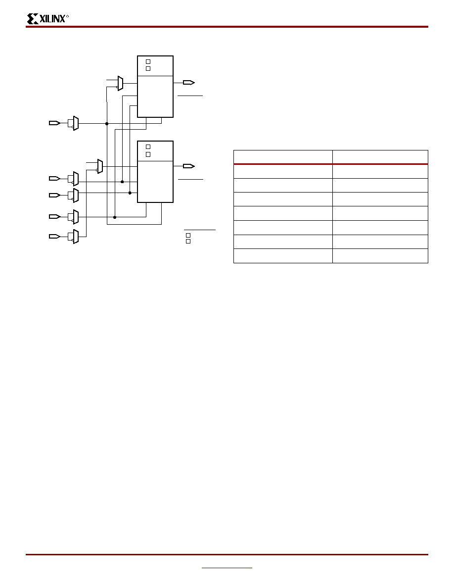
IOB blocks include six storage elements, as shown in
Figure 2
.
Each storage element can be configured either as an
edge-triggered D-type flip-flop or as a level-sensitive latch.
On the input, output, and 3-state path, one or two DDR reg-
isters can be used.
Double data rate is directly accomplished by the two regis-
ters on each path, clocked by the rising edges (or falling
edges) from two different clock nets. The two clock signals
are generated by the DCM and must be 180 degrees out of
phase, as shown in
Figure 3
. There are two input, output,
and 3-state data signals, each being alternately clocked out.
For each storage element, the SRHIGH, SRLOW, INIT0,
and INIT1 attributes are independent. Synchronous or
asynchronous set / reset is consistent in an IOB block.
All the control signals have independent polarity. Any
inverter placed on a control input is automatically absorbed.
Each register or latch (independent of all other registers or
latches) (see
Figure 4
) can be configured as follows:
∑
No set or reset
∑
Synchronous set
∑
Synchronous reset
∑
Synchronous set and reset
∑
Asynchronous set (preset)
∑
Asynchronous reset (clear)
∑
Asynchronous set and reset (preset and clear)
The synchronous reset overrides a set, and an asynchro-
nous clear overrides a preset.
Figure 2: Virtex-II IOB Block
Reg
OCK1
Reg
OCK2
Reg
ICK1
Reg
ICK2
DDR mux
Input
PAD
3-State
Reg
OCK1
Reg
OCK2
DDR mux
Output
IOB
DS031_29_100900
Figure 3: Double Data Rate Registers
D1
CLK1
DDR MUX
Q1
FDDR
D2
CLK2
(50/50 duty cycle clock)
CLOCK
Q
Q
Q2
D1
CLK1
DDR MUX
DCM
Q1
FDDR
D2
CLK2
Q2
180
∞ 0∞
DS031_26_100900
VirtexTM-II Platform FPGAs: Detailed Description
R
DS031-2 (v3.1) October 14, 2003
www.xilinx.com
Module 2 of 4
Product Specification
1-800-255-7778
4
Input/Output Individual Options
Each device pad has optional pull-up and pull-down in all
SelectI/O-Ultra configurations. Each device pad has
optional weak-keeper in LVTTL, LVCMOS, and PCI
SelectI/O-Ultra configurations, as illustrated in
Figure 5
.
Values of the optional pull-up and pull-down resistors are in
the range 10 - 60 K
, which is the specification for V
CCO
when operating at 3.3V (from 3.0 to 3.6V only). The clamp
diode is always present, even when power is not.
The optional weak-keeper circuit is connected to each user
I/O pad. When selected, the circuit monitors the voltage on
the pad and weakly drives the pin High or Low. If the pin is
connected to a multiple-source signal, the weak-keeper
Figure 4: Register / Latch Configuration in an IOB Block
FF
LATCH
SR REV
D1
Q1
CE
CK1
FF
LATCH
SR REV
D2
FF1
FF2
DDR MUX
Q2
CE
CK2
REV
SR
(O/T) CLK1
(OQ or TQ)
(O/T) CE
(O/T) 1
(O/T) CLK2
(O/T) 2
Attribute INIT1
INIT0
SRHIGH
SRLOW
Attribute INIT1
INIT0
SRHIGH
SRLOW
Reset Type
SYNC
ASYNC
DS031_25_110300
Shared
by all
registers
Figure 5: LVTTL, LVCMOS or PCI SelectI/O-Ultra Standards
VCCO
VCCO
VCCO
Weak
Keeper
Program
Delay
OBUF
IBUF
Program Current
Clamp
Diode
10-60K
10-60K
PAD
VCCAUX = 3.3V
DS031_23_011601
VCCINT = 1.5V

VirtexTM-II Platform FPGAs: Detailed Description
R
DS031-2 (v3.1) October 14, 2003
www.xilinx.com
Module 2 of 4
Product Specification
1-800-255-7778
5
holds the signal in its last state if all drivers are disabled.
Maintaining a valid logic level in this way eliminates bus
chatter. An enabled pull-up or pull-down overrides the
weak-keeper circuit.
LVTTL sinks and sources current up to 24 mA. The current
is programmable for LVTTL and LVCMOS SelectI/O-Ultra
standards (see
Table 4
). Drive-strength and slew-rate con-
trols for each output driver, minimize bus transients. For
LVDCI and LVDCI_DV2 standards, drive strength and
slew-rate controls are not available.
Figure 6
shows the SSTL2, SSTL3, and HSTL configura-
tions. HSTL can sink current up to 48 mA. (HSTL IV)
All pads are protected against damage from electrostatic
discharge (ESD) and from over-voltage transients. Virtex-II
uses two memory cells to control the configuration of an I/O
as an input. This is to reduce the probability of an I/O con-
figured as an input from flipping to an output when sub-
jected to a single event upset (SEU) in space applications.
Prior to configuration, all outputs not involved in configura-
tion are forced into their high-impedance state. The
pull-down resistors and the weak-keeper circuits are inac-
tive. The dedicated pin HSWAP_EN controls the pull-up
resistors prior to configuration. By default, HSWAP_EN is
set high, which disables the pull-up resistors on user I/O
pins. When HSWAP_EN is set low, the pull-up resistors are
activated on user I/O pins.
All Virtex-II IOBs support IEEE 1149.1 compatible boundary
scan testing.
Input Path
The Virtex-II IOB input path routes input signals directly to
internal logic and / or through an optional input flip-flop or
latch, or through the DDR input registers. An optional delay
element at the D-input of the storage element eliminates
pad-to-pad hold time. The delay is matched to the internal
clock-distribution delay of the Virtex-II device, and when
used, assures that the pad-to-pad hold time is zero.
Each input buffer can be configured to conform to any of the
low-voltage signaling standards supported. In some of
these standards the input buffer utilizes a user-supplied
threshold voltage, V
REF
. The need to supply V
REF
imposes
constraints on which standards can be used in the same
bank. See I/O banking description.
Output Path
The output path includes a 3-state output buffer that drives
the output signal onto the pad. The output and / or the
3-state signal can be routed to the buffer directly from the
internal logic or through an output / 3-state flip-flop or latch,
or through the DDR output / 3-state registers.
Each output driver can be individually programmed for a
wide range of low-voltage signaling standards. In most sig-
naling standards, the output High voltage depends on an
externally supplied V
CCO
voltage. The need to supply V
CCO
imposes constraints on which standards can be used in the
same bank. See I/O banking description.
I/O Banking
Some of the I/O standards described above require V
CCO
and V
REF
voltages. These voltages are externally supplied
and connected to device pins that serve groups of IOB
blocks, called banks. Consequently, restrictions exist about
which I/O standards can be combined within a given bank.
Eight I/O banks result from dividing each edge of the FPGA
into two banks, as shown in
Figure 7
and
Figure 8
. Each
bank has multiple V
CCO
pins, all of which must be con-
Table 4: LVTTL and LVCMOS Programmable Currents (Sink and Source)
SelectI/O-Ultra
Programmable Current (Worst-Case Guaranteed Minimum)
LVTTL
2 mA
4 mA
6 mA
8 mA
12 mA
16 mA
24 mA
LVCMOS33
2 mA
4 mA
6 mA
8 mA
12 mA
16 mA
24 mA
LVCMOS25
2 mA
4 mA
6 mA
8 mA
12 mA
16 mA
24 mA
LVCMOS18
2 mA
4 mA
6 mA
8 mA
12 mA
16 mA
n/a
LVCMOS15
2 mA
4 mA
6 mA
8 mA
12 mA
16 mA
n/a
Figure 6: SSTL or HSTL SelectI/O-Ultra Standards
VCCO
OBUF
VREF
Clamp
Diode
PAD
VCCAUX = 3.3V
VCCINT = 1.5V
DS031_24_100900
VirtexTM-II Platform FPGAs: Detailed Description
R
DS031-2 (v3.1) October 14, 2003
www.xilinx.com
Module 2 of 4
Product Specification
1-800-255-7778
6
nected to the same voltage. This voltage is determined by
the output standards in use.
Some input standards require a user-supplied threshold
voltage (V
REF
), and certain user-I/O pins are automatically
configured as V
REF
inputs. Approximately one in six of the
I/O pins in the bank assume this role.
V
REF
pins within a bank are interconnected internally, and
consequently only one V
REF
voltage can be used within
each bank. However, for correct operation, all V
REF
pins in
the bank must be connected to the external reference volt-
age source.
The V
CCO
and the V
REF
pins for each bank appear in the
device pinout tables. Within a given package, the number of
V
REF
and V
CCO
pins can vary depending on the size of
device. In larger devices, more I/O pins convert to V
REF
pins. Since these are always a superset of the V
REF
pins
used for smaller devices, it is possible to design a PCB that
permits migration to a larger device if necessary.
All V
REF
pins for the largest device anticipated must be con-
nected to the V
REF
voltage and not used for I/O. In smaller
devices, some V
CCO
pins used in larger devices do not con-
nect within the package. These unconnected pins can be
left unconnected externally, or, if necessary, they can be
connected to V
CCO
to permit migration to a larger device.
Rules for Combining I/O Standards in the Same Bank
The following rules must be obeyed to combine different
input, output, and bi-directional standards in the same bank:
1.
Combining output standards only. Output standards
with the same output V
CCO
requirement can be
combined in the same bank.
Compatible example:
SSTL2_I and LVDS_25_DCI outputs
Incompatible example:
SSTL2_I (output V
CCO
= 2.5V) and
LVCMOS33 (output V
CCO
= 3.3V) outputs
2.
Combining input standards only. Input standards
with the same input V
CCO
and input V
REF
requirements
can be combined in the same bank.
Compatible example:
LVCMOS15 and HSTL_IV inputs
Incompatible example:
LVCMOS15 (input V
CCO
= 1.5V) and
LVCMOS18 (input V
CCO
= 1.8V) inputs
Incompatible example:
HSTL_I_DCI_18 (V
REF
= 0.9V) and
HSTL_IV_DCI_18 (V
REF
= 1.1V) inputs
3.
Combining input standards and output standards.
Input standards and output standards with the same
input V
CCO
and output V
CCO
requirement can be
combined in the same bank.
Compatible example:
LVDS_25 output and HSTL_I input
Incompatible example:
LVDS_25 output (output V
CCO
= 2.5V) and
HSTL_I_DCI_18 input (input V
CCO
= 1.8V)
4.
Combining bi-directional standards with input or
output standards. When combining bi-directional I/O
with other standards, make sure the bi-directional
standard can meet rules 1 through 3 above.
5.
Additional rules for combining DCI I/O standards.
a.
No more than one Single Termination type (input or
output) is allowed in the same bank.
Incompatible example:
HSTL_IV_DCI input and HSTL_III_DCI input
b.
No more than one Split Termination type (input or
output) is allowed in the same bank.
Incompatible example:
HSTL_I_DCI input and HSTL_II_DCI input
The implementation tools will enforce these design rules.
Figure 7: Virtex-II I/O Banks: Top View for Wire-Bond
Packages (CS, FG, & BG)
Figure 8: Virtex-II I/O Banks: Top View for Flip-Chip
Packages (FF & BF)
ug002_c2_014_112900
Bank 0
Bank 1
Bank 5
Bank 4
Bank 7
Bank 6
Bank 2
Bank 3
ds031_66_112900
Bank 1
Bank 0
Bank 4
Bank 5
Bank 2
Bank 3
Bank 7
Bank 6
VirtexTM-II Platform FPGAs: Detailed Description
R
DS031-2 (v3.1) October 14, 2003
www.xilinx.com
Module 2 of 4
Product Specification
1-800-255-7778
7
Table 5
summarizes all standards and voltage supplies.
Table 5: Summary of Voltage Supply Requirements for
All Input and Output Standards
I/O Standard
V
CCO
V
REF
Termination Type
Output
Input
Input
Output
Input
LVDS_33
3.3
N/R
N/R
(1)
N/R
N/R
LVDSEXT_33
N/R
N/R
N/R
LVPECL_33
N/R
N/R
N/R
SSTL3_I
1.5
N/R
N/R
SSTL3_II
1.5
N/R
N/R
AGP
1.32
N/R
N/R
LVTTL
3.3
N/R
N/R
N/R
LVCMOS33
N/R
N/R
N/R
LVDCI_33
N/R
Series
N/R
LVDCI_DV2_33
N/R
Series
N/R
PCI33_3
N/R
N/R
N/R
PCI66_3
N/R
N/R
N/R
PCIX
N/R
N/R
N/R
LVDS_33_DCI
N/R
N/R
Split
LVDSEXT_33_DCI
N/R
N/R
Split
SSTL3_I_DCI
1.5
N/R
Split
SSTL3_II_DCI
1.5
Split
Split
LVDS_25
2.5
N/R
N/R
N/R
N/R
LVDSEXT_25
N/R
N/R
N/R
LDT_25
N/R
N/R
N/R
ULVDS_25
N/R
N/R
N/R
BLVDS_25
N/R
N/R
N/R
SSTL2_I
1.25
N/R
N/R
SSTL2_II
1.25
N/R
N/R
LVCMOS25
2.5
N/R
N/R
N/R
LVDCI_25
N/R
Series
N/R
LVDCI_DV2_25
N/R
Series
N/R
LVDS_25_DCI
N/R
N/R
Split
LVDSEXT_25_DCI
N/R
N/R
Split
SSTL2_I_DCI
1.25
N/R
Split
SSTL2_II_DCI
1.25
Split
Split
HSTL_III_18
1.8
N/R
1.1
N/R
N/R
HSTL_IV_18
1.1
N/R
N/R
HSTL_I_18
0.9
N/R
N/R
HSTL_II_18
0.9
N/R
N/R
SSTL18_I
0.9
N/R
N/R
SSTL18_II
0.9
N/R
N/R
LVCMOS18
1.8
N/R
N/R
N/R
LVDCI_18
N/R
Series
N/R
LVDCI_DV2_18
N/R
Series
N/R
HSTL_III_DCI_18
1.1
N/R
Single
HSTL_IV_DCI_18
1.1
Single
Single
HSTL_I_DCI_18
0.9
N/R
Split
HSTL_II_DCI_18
0.9
Split
Split
SSTL18_I_DCI
0.9
N/R
Split
SSTL18_II_DCI
0.9
Split
Split
HSTL_III
1.5
N/R
0.9
N/R
N/R
HSTL_IV
0.9
N/R
N/R
HSTL_I
0.75
N/R
N/R
HSTL_II
0.75
N/R
N/R
LVCMOS15
1.5
N/R
N/R
N/R
LVDCI_15
N/R
Series
N/R
LVDCI_DV2_15
N/R
Series
N/R
GTLP_DCI
1
Single
Single
HSTL_III_DCI
0.9
N/R
Single
HSTL_IV_DCI
0.9
Single
Single
HSTL_I_DCI
0.75
N/R
Split
HSTL_II_DCI
0.75
Split
Split
GTL_DCI
1.2
1.2
0.8
Single
Single
GTLP
N/R
N/R
1
N/R
N/R
GTL
0.8
N/R
N/R
Notes:
1.
N/R = no requirement.
Table 5: Summary of Voltage Supply Requirements for
All Input and Output Standards (Continued)
I/O Standard
V
CCO
V
REF
Termination Type
Output
Input
Input
Output
Input

VirtexTM-II Platform FPGAs: Detailed Description
R
DS031-2 (v3.1) October 14, 2003
www.xilinx.com
Module 2 of 4
Product Specification
1-800-255-7778
8
Digitally Controlled Impedance (DCI)
Today's chip output signals with fast edge rates require ter-
mination to prevent reflections and maintain signal integrity.
High pin count packages (especially ball grid arrays) can
not accommodate external termination resistors.
Virtex-II XCITE DCI provides controlled impedance drivers
and on-chip termination for single-ended and differential
I/Os. This eliminates the need for external resistors, and
improves signal integrity. The DCI feature can be used on
any IOB by selecting one of the DCI I/O standards.
When applied to inputs, DCI provides input parallel termina-
tion. When applied to outputs, DCI provides controlled
impedance drivers (series termination) or output parallel
termination.
DCI operates independently on each I/O bank. When a DCI
I/O standard is used in a particular I/O bank, external refer-
ence resistors must be connected to two dual-function pins
on the bank. These resistors, voltage reference of N transis-
tor (VRN) and the voltage reference of P transistor (VRP)
are shown in
Figure 9
.
When used with a terminated I/O standard, the value of
resistors are specified by the standard (typically 50
).
When used with a controlled impedance driver, the resistors
set the output impedance of the driver within the specified
range (25
to 100 ). For all series and parallel termina-
tions listed in
Table 6
and
Table 7
, the reference resistors
must have the same value for any given bank. One percent
resistors are recommended.
The DCI system adjusts the I/O impedance to match the two
external reference resistors, or half of the reference resis-
tors, and compensates for impedance changes due to volt-
age and/or temperature fluctuations. The adjustment is
done by turning parallel transistors in the IOB on or off.
Controlled Impedance Drivers (Series
Termination)
DCI can be used to provide a buffer with a controlled output
impedance. It is desirable for this output impedance to
match the transmission line impedance (Z). Virtex-II input
buffers also support LVDCI and LVDCI_DV2 I/O standards.
Controlled Impedance Drivers (Parallel
Termination)
DCI also provides on-chip termination for SSTL3, SSTL2,
HSTL (Class I, II, III, or IV), and GTL/GTLP receivers or
transmitters on bidirectional lines.
Table 7
lists the on-chip parallel terminations available in Vir-
tex-II devices. V
CCO
must be set according to
Table 3
. Note
that there is a V
CCO
requirement for GTL_DCI and
GTLP_DCI, due to the on-chip termination resistor.
Figure 9: DCI in a Virtex-II Bank
DS031_50_101200
VCCO
GND
DCI
DCI
DCI
DCI
VRN
VRP
1 Bank
R
REF
(1%)
R
REF
(1%)
Figure 10: Internal Series Termination
Table 6: SelectI/O-Ultra Controlled Impedance Buffers
V
CCO
DCI
DCI Half Impedance
3.3 V
LVDCI_33
LVDCI_DV2_33
2.5 V
LVDCI_25
LVDCI_DV2_25
1.8 V
LVDCI_18
LVDCI_DV2_18
1.5 V
LVDCI_15
LVDCI_DV2_15
Table 7: SelectI/O-Ultra Buffers With On-Chip Parallel
Termination
I/O Standard
External
Termination
On-Chip
Termination
SSTL3 Class I
SSTL3_I
SSTL3_I_DCI
(1)
SSTL3 Class II
SSTL3_II
SSTL3_II_DCI
(1)
SSTL2 Class I
SSTL2_I
SSTL2_I_DCI
(1)
SSTL2 Class II
SSTL2_II
SSTL2_II_DCI
(1)
HSTL Class I
HSTL_I
HSTL_I_DCI
HSTL Class II
HSTL_II
HSTL_II_DCI
HSTL Class III
HSTL_III
HSTL_III_DCI
HSTL Class IV
HSTL_IV
HSTL_IV_DCI
GTL
GTL
GTL_DCI
GTLP
GTLP
GTLP_DCI
Notes:
1.
SSTL Compatible
Z
IOB
Z
Virtex-II DCI
DS031_51_110600
V
CCO
= 3.3 V, 2.5 V, 1.8 V or 1.5 V
VirtexTM-II Platform FPGAs: Detailed Description
R
DS031-2 (v3.1) October 14, 2003
www.xilinx.com
Module 2 of 4
Product Specification
1-800-255-7778
9
Figure 11
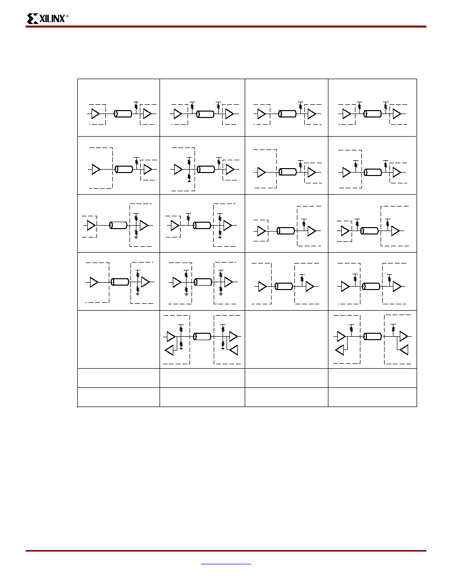
provides examples illustrating the use of the HSTL_I_DCI, HSTL_II_DCI, HSTL_III_DCI, and HSTL_IV_DCI I/O
standards. For a complete list, see the Virtex-II User Guide.
Figure 11: HSTL DCI Usage Examples
Virtex-II DCI
R
R
VCCO
VCCO
R
R
VCCO
VCCO
R
VCCO
R
VCCO
Virtex-II DCI
Virtex-II DCI
R
VCCO
R
VCCO
Virtex-II DCI
R
R
VCCO/2
VCCO/2
2R
Virtex-II DCI
2R
R
VCCO
VCCO/2
Virtex-II DCI
2R
R
VCCO/2
2R
VCCO
2R
Virtex-II DCI
2R
VCCO
Virtex-II DCI
2R
2R
VCCO
DS031_65a_100201
Conventional
DCI Transmit
Conventional
Receive
Conventional
Transmit
DCI Receive
DCI Transmit
DCI Receive
Bidirectional
Reference
Resistor
Recommended
Z0
(1)
VRN = VRP = R = Z0
50
VRN = VRP = R = Z0
50
VRN = VRP = R = Z0
50
VRN = VRP = R = Z0
50
HSTL_I
HSTL_II
HSTL_III
HSTL_IV
N/A
N/A
Virtex-II DCI
R
VCCO
R
VCCO
R
VCCO
Virtex-II DCI
R
VCCO
Virtex-II DCI
Z0
R
VCCO/2
Virtex-II DCI
R
VCCO/2
Virtex-II DCI
2R
2R
VCCO
Virtex-II DCI
Virtex-II DCI
2R
2R
VCCO
Z0
Z0
Z0
Z0
Z0
Z0
Z0
Z0
Z0
Z0
Z0
Z0
Z0
Z0
Z0
Virtex-II DCI
Virtex-II DCI
Z0
Virtex-II DCI
2R
2R
VCCO
2R
2R
VCCO
Virtex-II DCI
Z0
Virtex-II DCI
R
VCCO
R
VCCO
Note:
1. Z0 is the recommended PCB trace impedance.

VirtexTM-II Platform FPGAs: Detailed Description
R
DS031-2 (v3.1) October 14, 2003
www.xilinx.com
Module 2 of 4
Product Specification
1-800-255-7778
10
Figure 12
provides examples illustrating the use of the SSTL2_I_DCI, SSTL2_II_DCI, SSTL3_I_DCI, and SSTL3_II_DCI I/O
standards. For a complete list, see the Virtex-II User Guide.
Figure 12: SSTL DCI Usage Examples
DS031_65b_112502
Conventional
DCI Transmit
Conventional
Receive
Conventional
Transmit
DCI Receive
DCI Transmit
DCI Receive
Bidirectional
Reference
Resistor
Recommended
Z0
(2)
VRN = VRP = R = Z0
50
VRN = VRP = R = Z0
50
VRN = VRP = R = Z0
50
VRN = VRP = R = Z0
50
SSTL2_I
SSTL2_II
SSTL3_I
SSTL3_II
N/A
N/A
Virtex-II DCI
Z0
R
V
CCO
/2
Z0
R/2
R
R
VCCO/2
VCCO/2
Z0
R/2
R
R
VCCO/2
VCCO/2
Z0
R/2
R
V
CCO
/2
Z0
R/2
R
VCCO/2
Z0
R/2
Virtex-II DCI
2R
2R
VCCO
R
VCCO/2
Z0
R/2
Virtex-II DCI
2R
2R
VCCO
Z0
R/2
Virtex-II DCI
2R
2R
VCCO
Z0
R/2
Virtex-II DCI
2R
2R
VCCO
Virtex-II DCI
R
VCCO
VCCO/2
2R
Virtex-II DCI
R
VCCO
VCCO/2
2R
Virtex-II DCI
R
VCCO/2
Z0
Z0
Z0
Virtex-II DCI
R
V
CCO
/2
Z0
2R
2R
2R
Virtex-II DCI
2R
VCCO
Virtex-II DCI
2R
2R
VCCO
Z0
Virtex-II DCI
Virtex-II DCI
2R
2R
VCCO
Z0
2R
Virtex-II DCI
2R
VCCO
Virtex-II DCI
2R
2R
VCCO
Z0
Virtex-II DCI
2R
2R
VCCO
Virtex-II DCI
Z0
Virtex-II DCI
2R
2R
VCCO
2R
2R
VCCO
Virtex-II DCI
Z0
Virtex-II DCI
2R
2R
VCCO
2R
2R
VCCO
25
(1)
25
(1)
25
(1)
25
(1)
25
(1)
25
(1)
25
(1)
25
(1)
25
(1)
25
(1)
25
(1)
25
(1)
Notes:
1. The SSTL-compatible 25
series resistor is accounted for in the DCI buffer, and it is not DCI controlled.
2. Z0 is the recommended PCB trace impedance.
VirtexTM-II Platform FPGAs: Detailed Description
R
DS031-2 (v3.1) October 14, 2003
www.xilinx.com
Module 2 of 4
Product Specification
1-800-255-7778
11
Figure 13
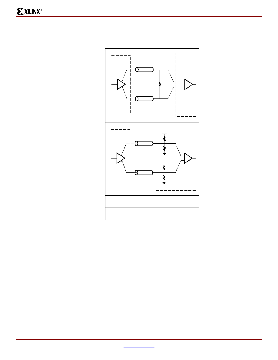
provides examples illustrating the use of the LVDS_DCI and LVDSEXT_DCI I/O standards. For a complete list,
see the Virtex-II User Guide.
Figure 13: LVDS DCI Usage Examples
DS031_65c_022103
Conventional
Conventional
Transmit
DCI Receive
Reference
Resistor
Recommended
Z0
VRN = VRP = R = Z0
50
LVDS_DCI and LVDSEXT_DCI Receiver
Virtex-II
LVDS DCI
Z0
2R
2R
V
CCO
Z0
2R
2R
V
CCO
Virtex-II
LVDS
Z0
2R
Z0
NOTE: Only LVDS25_DCI is supported (V
CCO
= 2.5V only)
VirtexTM-II Platform FPGAs: Detailed Description
R
DS031-2 (v3.1) October 14, 2003
www.xilinx.com
Module 2 of 4
Product Specification
1-800-255-7778
12
Configurable Logic Blocks (CLBs)
The Virtex-II configurable logic blocks (CLB) are organized
in an array and are used to build combinatorial and synchro-
nous logic designs. Each CLB element is tied to a switch
matrix to access the general routing matrix, as shown in
Figure 14
. A CLB element comprises 4 similar slices, with
fast local feedback within the CLB. The four slices are split
in two columns of two slices with two independent carry
logic chains and one common shift chain.
Slice Description
Each slice includes two 4-input function generators, carry
logic, arithmetic logic gates, wide function multiplexers and
two storage elements. As shown in
Figure 15
, each 4-input
function generator is programmable as a 4-input LUT, 16
bits of distributed SelectRAM memory, or a 16-bit vari-
able-tap shift register element.
The output from the function generator in each slice drives
both the slice output and the D input of the storage element.
Figure 16
shows a more detailed view of a single slice.
Configurations
Look-Up Table
Virtex-II function generators are implemented as 4-input
look-up tables (LUTs). Four independent inputs are pro-
vided to each of the two function generators in a slice (F and
G). These function generators are each capable of imple-
menting any arbitrarily defined boolean function of four
inputs. The propagation delay is therefore independent of
the function implemented. Signals from the function gener-
ators can exit the slice (X or Y output), can input the XOR
dedicated gate (see arithmetic logic), or input the carry-logic
multiplexer (see fast look-ahead carry logic), or feed the D
input of the storage element, or go to the MUXF5 (not
shown in
Figure 16
).
In addition to the basic LUTs, the Virtex-II slice contains
logic (MUXF5 and MUXFX multiplexers) that combines
function generators to provide any function of five, six,
seven, or eight inputs. The MUXFX are either MUXF6,
MUXF7 or MUXF8 according to the slice considered in the
CLB. Selected functions up to nine inputs (MUXF5 multi-
plexer) can be implemented in one slice. The MUXFX can
also be a MUXF6, MUXF7, or MUXF8 multiplexers to map
any functions of six, seven, or eight inputs and selected
wide logic functions.
Register/Latch
The storage elements in a Virtex-II slice can be configured
either as edge-triggered D-type flip-flops or as level-sensi-
tive latches. The D input can be directly driven by the X or Y
output via the DX or DY input, or by the slice inputs bypass-
ing the function generators via the BX or BY input. The clock
enable signal (CE) is active High by default. If left uncon-
nected, the clock enable for that storage element defaults to
the active state.
In addition to clock (CK) and clock enable (CE) signals,
each slice has set and reset signals (SR and BY slice
inputs). SR forces the storage element into the state speci-
fied by the attribute SRHIGH or SRLOW. SRHIGH forces a
logic "1" when SR is asserted. SRLOW forces a logic "0".
When SR is used, a second input (BY) forces the storage
element into the opposite state. The reset condition is pre-
dominant over the set condition. (See
Figure 17
.)
The initial state after configuration or global initial state is
defined by a separate INIT0 and INIT1 attribute. By default,
setting the SRLOW attribute sets INIT0, and setting the
SRHIGH attribute sets INIT1.
For each slice, set and reset can be set to be synchronous
or asynchronous. Virtex-II devices also have the ability to
set INIT0 and INIT1 independent of SRHIGH and SRLOW.
The control signals clock (CLK), clock enable (CE) and
set/reset (SR) are common to both storage elements in one
slice. All of the control signals have independent polarity. Any
inverter placed on a control input is automatically absorbed.
Figure 14: Virtex-II CLB Element
Figure 15: Virtex-II Slice Configuration
Slice
X1Y1
Slice
X1Y0
Slice
X0Y1
Slice
X0Y0
Fast
Connects
to neighbors
Switch
Matrix
DS031_32_101600
SHIFT
CIN
COUT
TBUF X0Y1
COUT
CIN
TBUF X0Y0
Register
MUXF5
MUXFx
CY
SRL16
RAM16
LUT
G
Register
Arithmetic Logic
CY
LUT
F
DS031_31_100900
SRL16
RAM16
ORCY

VirtexTM-II Platform FPGAs: Detailed Description
R
DS031-2 (v3.1) October 14, 2003
www.xilinx.com
Module 2 of 4
Product Specification
1-800-255-7778
13
Figure 16: Virtex-II Slice (Top Half)
G4
SOPIN
A4
G3
A3
G2
A2
G1
A1
WG4
WG4
WG3
WG3
WG2
WG2
WG1
BY
WG1
Dual-Port
LUT
FF
LATCH
RAM
ROM
Shift-Reg
D
0
MC15
WS
SR
SR
REV
DI
G
Y
G2
G1
BY
1
0
PROD
D
Q
CE
CE
CK
CLK
MUXCY
YB
DIG
DY
Y
0
1
MUXCY
0
1
1
SOPOUT
DYMUX
GYMUX
YBMUX
ORCY
WSG
WE[2:0]
SHIFTOUT
CYOG
XORG
WE
CLK
WSF
ALTDIG
CE
SR
CLK
SLICEWE[2:0]
MULTAND
Shared between
x & y Registers
SHIFTIN
COUT
CIN
DS031_01_112502
Q
VirtexTM-II Platform FPGAs: Detailed Description
R
DS031-2 (v3.1) October 14, 2003
www.xilinx.com
Module 2 of 4
Product Specification
1-800-255-7778
14
The set and reset functionality of a register or a latch can be
configured as follows:
∑
No set or reset
∑
Synchronous set
∑
Synchronous reset
∑
Synchronous set and reset
∑
Asynchronous set (preset)
∑
Asynchronous reset (clear)
∑
Asynchronous set and reset (preset and clear)
The synchronous reset has precedence over a set, and an
asynchronous clear has precedence over a preset.
Distributed SelectRAM Memory
Each function generator (LUT) can implement a 16 x 1-bit
synchronous RAM resource called a distributed SelectRAM
element. The SelectRAM elements are configurable within
a CLB to implement the following:
∑
Single-Port 16 x 8 bit RAM
∑
Single-Port 32 x 4 bit RAM
∑
Single-Port 64 x 2 bit RAM
∑
Single-Port 128 x 1 bit RAM
∑
Dual-Port 16 x 4 bit RAM
∑
Dual-Port 32 x 2 bit RAM
∑
Dual-Port 64 x 1 bit RAM
Distributed SelectRAM memory modules are synchronous
(write) resources. The combinatorial read access time is
extremely fast, while the synchronous write simplifies
high-speed designs. A synchronous read can be imple-
mented with a storage element in the same slice. The dis-
tributed SelectRAM memory and the storage element share
the same clock input. A Write Enable (WE) input is active
High, and is driven by the SR input.
Table 8
shows the number of LUTs (2 per slice) occupied by
each distributed SelectRAM configuration.
For single-port configurations, distributed SelectRAM mem-
ory has one address port for synchronous writes and asyn-
chronous reads.
For dual-port configurations, distributed SelectRAM mem-
ory has one port for synchronous writes and asynchronous
reads and another port for asynchronous reads. The func-
tion generator (LUT) has separated read address inputs
(A1, A2, A3, A4) and write address inputs (WG1/WF1,
WG2/WF2, WG3/WF3, WG4/WF4).
In single-port mode, read and write addresses share the
same address bus. In dual-port mode, one function genera-
tor (R/W port) is connected with shared read and write
addresses. The second function generator has the A inputs
(read) connected to the second read-only port address and
the W inputs (write) shared with the first read/write port
address.
Figure 17: Register / Latch Configuration in a Slice
FF
FFY
LATCH
SR REV
D
Q
CE
CK
YQ
FF
FFX
LATCH
SR REV
D
Q
CE
CK
XQ
CE
DX
DY
BY
CLK
BX
SR
Attribute
INIT1
INIT0
SRHIGH
SRLOW
Attribute
INIT1
INIT0
SRHIGH
SRLOW
Reset Type
SYNC
ASYNC
DS031_22_110600
Table 8: Distributed SelectRAM Configurations
RAM
Number of LUTs
16 x 1S
1
16 x 1D
2
32 x 1S
2
32 x 1D
4
64 x 1S
4
64 x 1D
8
128 x 1S
8
Notes:
1.
S = single-port configuration; D = dual-port configuration
VirtexTM-II Platform FPGAs: Detailed Description
R
DS031-2 (v3.1) October 14, 2003
www.xilinx.com
Module 2 of 4
Product Specification
1-800-255-7778
15
Figure 18
,
Figure 19
, and
Figure 20
illustrate various exam-
ple configurations.
Similar to the RAM configuration, each function generator
(LUT) can implement a 16 x 1-bit ROM. Five configurations
are available: ROM16x1, ROM32x1, ROM64x1,
ROM128x1, and ROM256x1. The ROM elements are cas-
cadable to implement wider or/and deeper ROM. ROM con-
tents are loaded at configuration.
Table 9
shows the number
of LUTs occupied by each configuration.
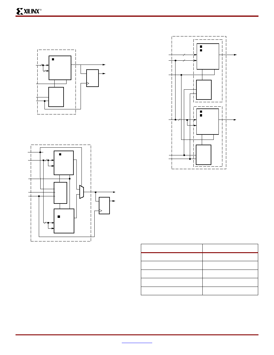
Figure 18: Distributed SelectRAM (RAM16x1S)
Figure 19: Single-Port Distributed SelectRAM
(RAM32x1S)
A[3:0]
D
D
DI
WS
WSG
WE
WCLK
RAM 16x1S
D
Q
RAM
WE
CK
A[4:1]
WG[4:1]
Output
Registered
Output
(optional)
(SR)
4
4
(BY)
DS031_02_100900
A[3:0]
D
WSG
F5MUX
WE
WCLK
RAM 32x1S
D Q
WE
WE0
CK
WSF
D
DI
WS
RAM
G[4:1]
A[4]
WG[4:1]
D
DI
WS
RAM
F[4:1]
WF[4:1]
Output
Registered
Output
(optional)
(SR)
4
(BY)
(BX)
4
DS031_03_110100
Figure 20: Dual-Port Distributed SelectRAM
(RAM16x1D)
Table 9: ROM Configuration
ROM
Number of LUTs
16 x 1
1
32 x 1
2
64 x 1
4
128 x 1
8 (1 CLB)
256 x 1
16 (2 CLBs)
A[3:0]
D
WSG
WE
WCLK
RAM 16x1D
WE
CK
D
DI
WS
RAM
G[4:1]
WG[4:1]
dual_port
RAM
dual_port
4
(BY)
DPRA[3:0]
SPO
A[3:0]
WSG
WE
CK
D
DI
WS
G[4:1]
WG[4:1]
DPO
4
4
DS031_04_110100
(SR)

VirtexTM-II Platform FPGAs: Detailed Description
R
DS031-2 (v3.1) October 14, 2003
www.xilinx.com
Module 2 of 4
Product Specification
1-800-255-7778
16
Shift Registers
Each function generator can also be configured as a 16-bit
shift register. The write operation is synchronous with a
clock input (CLK) and an optional clock enable, as shown in
Figure 21
. A dynamic read access is performed through the
4-bit address bus, A[3:0]. The configurable 16-bit shift regis-
ter cannot be set or reset. The read is asynchronous, how-
ever the storage element or flip-flop is available to
implement a synchronous read. The storage element
should always be used with a constant address. For exam-
ple, when building an 8-bit shift register and configuring the
addresses to point to the 7th bit, the 8th bit can be the
flip-flop. The overall system performance is improved by
using the superior clock-to-out of the flip-flops.
An additional dedicated connection between shift registers
allows connecting the last bit of one shift register to the first
bit of the next, without using the ordinary LUT output. (See
Figure 22
.) Longer shift registers can be built with dynamic
access to any bit in the chain. The shift register chaining
and the MUXF5, MUXF6, and MUXF7 multiplexers allow up
to a 128-bit shift register with addressable access to be
implemented in one CLB.
Figure 21: Shift Register Configurations
A[3:0]
SHIFTIN
SHIFTOUT
D(BY)
D
MC15
DI
WSG
CE (SR)
CLK
SRLC16
D
Q
SHIFT-REG
WE
CK
A[4:1]
Output
Registered
Output
(optional)
4
DS031_05_110600
WS
Figure 22: Cascadable Shift Register
SRLC16
MC15
MC15
D
SRLC16
DI
SHIFTIN
CASCADABLE OUT
SLICE S0
SLICE S1
SLICE S2
SLICE S3
1 Shift Chain
in CLB
CLB
DS031_06_110200
FF
FF
D
SRLC16
MC15
MC15
D
SRLC16
DI
SHIFTIN
SHIFTOUT
FF
FF
D
SRLC16
MC15
MC15
D
SRLC16
DI
DI
SHIFTIN
IN
SHIFTOUT
FF
FF
D
SRLC16
MC15
MC15
D
SRLC16
DI
SHIFTOUT
FF
FF
D
DI
DI
DI
OUT
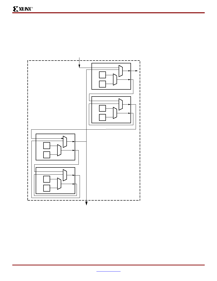
VirtexTM-II Platform FPGAs: Detailed Description
R
DS031-2 (v3.1) October 14, 2003
www.xilinx.com
Module 2 of 4
Product Specification
1-800-255-7778
17
Multiplexers
Virtex-II function generators and associated multiplexers
can implement the following:
∑
4:1 multiplexer in one slice
∑
8:1 multiplexer in two slices
∑
16:1 multiplexer in one CLB element (4 slices)
∑
32:1 multiplexer in two CLB elements (8 slices)
Each Virtex-II slice has one MUXF5 multiplexer and one
MUXFX multiplexer. The MUXFX multiplexer implements
the MUXF6, MUXF7, or MUXF8, as shown in
Figure 23
.
Each CLB element has two MUXF6 multiplexers, one
MUXF7 multiplexer and one MUXF8 multiplexer. Examples
of multiplexers are shown in the Virtex-II User Guide. Any
LUT can implement a 2:1 multiplexer.
Fast Lookahead Carry Logic
Dedicated carry logic provides fast arithmetic addition and
subtraction. The Virtex-II CLB has two separate carry
chains, as shown in the
Figure 24
.
The height of the carry chains is two bits per slice. The carry
chain in the Virtex-II device is running upward. The dedi-
cated carry path and carry multiplexer (MUXCY) can also
be used to cascade function generators for implementing
wide logic functions.
Arithmetic Logic
The arithmetic logic includes an XOR gate that allows a
2-bit full adder to be implemented within a slice. In addition,
a dedicated AND (MULT_AND) gate (shown in
Figure 16
)
improves the efficiency of multiplier implementation.
Figure 23: MUXF5 and MUXFX multiplexers
Slice S1
Slice S0
Slice S3
Slice S2
CLB
DS031_08_100201
F5
F6
F5
F7
F5
F6
F5
F8
MUXF8 combines
the two MUXF7 outputs
(Two CLBs)
MUXF6 combines the two MUXF5
outputs from slices S2 and S3
MUXF7 combines the two MUXF6
outputs from slices S0 and S2
MUXF6 combines the two MUXF5
outputs from slices S0 and S1
G
F
G
F
G
F
G
F
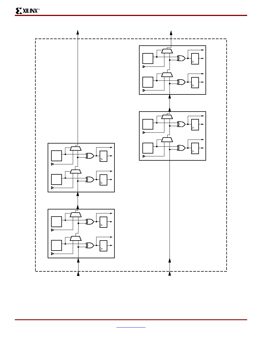
VirtexTM-II Platform FPGAs: Detailed Description
R
DS031-2 (v3.1) October 14, 2003
www.xilinx.com
Module 2 of 4
Product Specification
1-800-255-7778
18
Figure 24: Fast Carry Logic Path
FF
LUT
O I
MUXCY
FF
LUT
O I
MUXCY
FF
LUT
O I
MUXCY
FF
LUT
O I
MUXCY
CIN
CIN
CIN
COUT
FF
LUT
O I
MUXCY
FF
LUT
O I
MUXCY
FF
LUT
O I
MUXCY
FF
LUT
O I
MUXCY
CIN
COUT
COUT
to CIN of S2 of the next CLB
COUT
to S0 of the next CLB
(First Carry Chain)
(Second Carry Chain)
SLICE S1
SLICE S0
SLICE S3
SLICE S2
CLB
DS031_07_110200

VirtexTM-II Platform FPGAs: Detailed Description
R
DS031-2 (v3.1) October 14, 2003
www.xilinx.com
Module 2 of 4
Product Specification
1-800-255-7778
19
Sum of Products
Each Virtex-II slice has a dedicated OR gate named ORCY,
ORing together outputs from the slices carryout and the ORCY
from an adjacent slice. The ORCY gate with the dedicated
Sum of Products (SOP) chain are designed for implementing
large, flexible SOP chains. One input of each ORCY is con-
nected through the fast SOP chain to the output of the previous
ORCY in the same slice row. The second input is connected to
the output of the top MUXCY in the same slice, as shown in
Figure 25
.
LUTs and MUXCYs can implement large AND gates or
other combinatorial logic functions.
Figure 26
illustrates
LUT and MUXCY resources configured as a 16-input AND
gate.
Figure 25: Horizontal Cascade Chain
MUXCY
4
MUXCY
4
Slice 1
ds031_64_110300
ORCY
LUT
LUT
MUXCY
4
MUXCY
4
Slice 0
V
CC
LUT
LUT
MUXCY
4
MUXCY
4
Slice 3
ORCY
LUT
LUT
MUXCY
4
MUXCY
4
Slice 2
V
CC
LUT
LUT
SOP
CLB
MUXCY
4
MUXCY
4
Slice 1
ORCY
LUT
LUT
MUXCY
4
MUXCY
4
Slice 0
V
CC
LUT
LUT
MUXCY
4
MUXCY
4
Slice 3
ORCY
LUT
LUT
MUXCY
4
MUXCY
4
Slice 2
V
CC
LUT
LUT
CLB
Figure 26: Wide-Input AND Gate (16 Inputs)
MUXCY
AND
4
16
MUXCY
4
"0"
0
1
0
1
"0"
0
1
"0"
MUXCY
4
Slice
OUT
OUT
Slice
LUT
DS031_41_110600
LUT
LUT
VCC
MUXCY
4
0
1
LUT
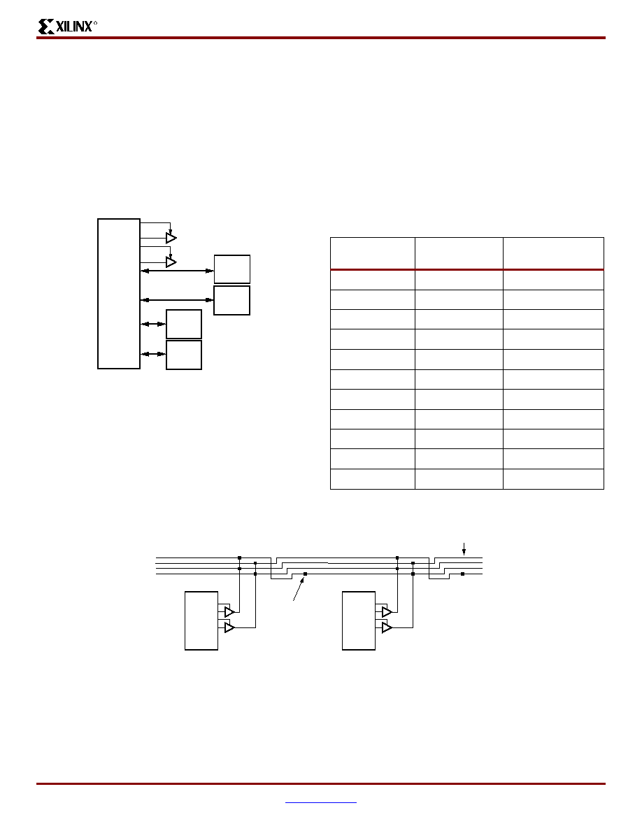
VirtexTM-II Platform FPGAs: Detailed Description
R
DS031-2 (v3.1) October 14, 2003
www.xilinx.com
Module 2 of 4
Product Specification
1-800-255-7778
20
3-State Buffers
Introduction
Each Virtex-II CLB contains two 3-state drivers (TBUFs)
that can drive on-chip busses. Each 3-state buffer has its
own 3-state control pin and its own input pin.
Each of the four slices have access to the two 3-state buff-
ers through the switch matrix, as shown in
Figure 27
.
TBUFs in neighboring CLBs can access slice outputs by
direct connects. The outputs of the 3-state buffers drive hor-
izontal routing resources used to implement 3-state busses.
The 3-state buffer logic is implemented using AND-OR logic
rather than 3-state drivers, so that timing is more predict-
able and less load dependant especially with larger devices.
Locations / Organization
Four horizontal routing resources per CLB are provided for
on-chip 3-state busses. Each 3-state buffer has access
alternately to two horizontal lines, which can be partitioned
as shown in
Figure 28
. The switch matrices corresponding
to SelectRAM memory and multiplier or I/O blocks are
skipped.
Number of 3-State Buffers
Table 10
shows the number of 3-state buffers available in
each Virtex-II device. The number of 3-state buffers is twice
the number of CLB elements.
CLB/Slice Configurations
Table 11
summarizes the logic resources in one CLB. All of the CLBs are identical and each CLB or slice can be
implemented in one of the configurations listed.
Table 12
shows the available resources in all CLBs.
Figure 27: Virtex-II 3-State Buffers
Slice
S3
Slice
S2
Slice
S1
Slice
S0
Switch
Matrix
DS031_37_060700
TBUF
TBUF
Table 10: Virtex-II 3-State Buffers
Device
3-State Buffers
per Row
Total Number
of 3-State Buffers
XC2V40
16
128
XC2V80
16
256
XC2V250
32
768
XC2V500
48
1,536
XC2V1000
64
2,560
XC2V1500
80
3,840
XC2V2000
96
5,376
XC2V3000
112
7,168
XC2V4000
144
11,520
XC2V6000
176
16,896
XC2V8000
208
23,296
Figure 28: 3-State Buffer Connection to Horizontal Lines
Switch
matrix
CLB-II
Switch
matrix
CLB-II
DS031_09_032700
Programmable
connection
3 - state lines
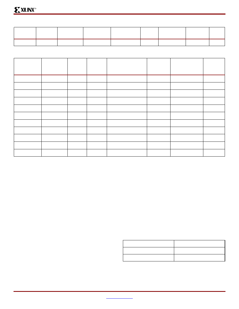
VirtexTM-II Platform FPGAs: Detailed Description
R
DS031-2 (v3.1) October 14, 2003
www.xilinx.com
Module 2 of 4
Product Specification
1-800-255-7778
21
18 Kbit Block SelectRAM
Resources
Introduction
Virtex-II devices incorporate large amounts of 18 Kbit block
SelectRAM. These complement the distributed SelectRAM
resources that provide shallow RAM structures imple-
mented in CLBs. Each Virtex-II block SelectRAM is an 18
Kbit true dual-port RAM with two independently clocked and
independently controlled synchronous ports that access a
common storage area. Both ports are functionally identical.
CLK, EN, WE, and SSR polarities are defined through con-
figuration.
Each port has the following types of inputs: Clock and Clock
Enable, Write Enable, Set/Reset, and Address, as well as
separate Data/parity data inputs (for write) and Data/parity
data outputs (for read).
Operation is synchronous; the block SelectRAM behaves
like a register. Control, address and data inputs must (and
need only) be valid during the set-up time window prior to a
rising (or falling, a configuration option) clock edge. Data
outputs change as a result of the same clock edge.
Configuration
The Virtex-II block SelectRAM supports various configura-
tions, including single- and dual-port RAM and various
data/address aspect ratios. Supported memory configura-
tions for single- and dual-port modes are shown in
Table 13
.
Table 11: Logic Resources in One CLB
Slices
LUTs
Flip-Flops
MULT_ANDs
Arithmetic &
Carry-Chains
SOP
Chains
Distributed
SelectRAM
Shift
Registers
TBUF
4
8
8
8
2
2
128 bits
128 bits
2
Table 12: Virtex-II Logic Resources Available in All CLBs
Device
CLB Array:
Row x
Column
Number
of
Slices
Number
of
LUTs
Max Distributed
SelectRAM or Shift
Register (bits)
Number
of
Flip-Flops
Number
of
Carry-Chains
(1)
Number
of SOP
Chains
(1)
XC2V40
8 x 8
256
512
8,192
512
16
16
XC2V80
16 x 8
512
1,024
16,384
1,024
16
32
XC2V250
24 x 16
1,536
3,072
49,152
3,072
32
48
XC2V500
32 x 24
3,072
6,144
98,304
6,144
48
64
XC2V1000
40 x 32
5,120
10,240
163,840
10,240
64
80
XC2V1500
48 x 40
7,680
15,360
245,760
15,360
80
96
XC2V2000
56 x 48
10,752
21,504
344,064
21,504
96
112
XC2V3000
64 x 56
14,336
28,672
458,752
28,672
112
128
XC2V4000
80 x 72
23,040
46,080
737,280
46,080
144
160
XC2V6000
96 x 88
33,792
67,584
1,081,344
67,584
176
192
XC2V8000
112 x 104
46,592
93,184
1,490,944
93,184
208
224
Notes:
1.
The carry-chains and SOP chains can be split or cascaded.
Table 13: Dual- and Single-Port Configurations
16K x 1 bit
2K x 9 bits
8K x 2 bits
1K x 18 bits
4K x 4 bits
512 x 36 bits
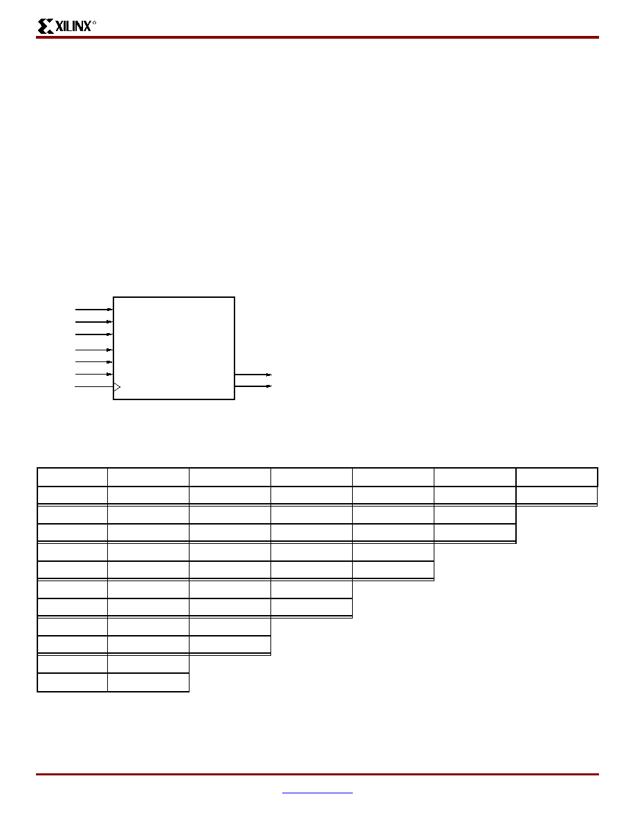
VirtexTM-II Platform FPGAs: Detailed Description
R
DS031-2 (v3.1) October 14, 2003
www.xilinx.com
Module 2 of 4
Product Specification
1-800-255-7778
22
Single-Port Configuration
As a single-port RAM, the block SelectRAM has access to
the 18 Kbit memory locations in any of the 2K x 9-bit,
1K x 18-bit, or 512 x 36-bit configurations and to 16 Kbit
memory locations in any of the 16K x 1-bit, 8K x 2-bit, or
4K x 4-bit configurations. The advantage of the 9-bit, 18-bit
and 36-bit widths is the ability to store a parity bit for each
eight bits. Parity bits must be generated or checked exter-
nally in user logic. In such cases, the width is viewed as 8 +
1, 16 + 2, or 32 + 4. These extra parity bits are stored and
behave exactly as the other bits, including the timing param-
eters. Video applications can use the 9-bit ratio of Virtex-II
block SelectRAM memory to advantage.
Each block SelectRAM cell is a fully synchronous memory
as illustrated in
Figure 29
. Input data bus and output data
bus widths are identical.
Dual-Port Configuration
As a dual-port RAM, each port of block SelectRAM has
access to a common 18 Kbit memory resource. These are
fully synchronous ports with independent control signals for
each port. The data widths of the two ports can be config-
ured independently, providing built-in bus-width conversion.
Table 14
illustrates the different configurations available on
ports A & B.
If both ports are configured in either 2K x 9-bit, 1K x 18-bit,
or 512 x 36-bit configurations, the 18 Kbit block is accessi-
ble from port A or B. If both ports are configured in either
16K x 1-bit, 8K x 2-bit. or 4K x 4-bit configurations, the
16 K-bit block is accessible from Port A or Port B. All other
configurations result in one port having access to an 18 Kbit
memory block and the other port having access to a 16 K-bit
subset of the memory block equal to 16 Kbits.
Figure 29: 18 Kbit Block SelectRAM Memory in
Single-Port Mode
DOP
DIP
ADDR
WE
EN
SSR
CLK
18 Kbit Block SelectRAM
DS031_10_071602
DI
DO
Table 14: Dual-Port Mode Configurations
Port A
16K x 1
16K x 1
16K x 1
16K x 1
16K x 1
16K x 1
Port B
16K x 1
8K x 2
4K x 4
2K x 9
1K x 18
512 x 36
Port A
8K x 2
8K x 2
8K x 2
8K x 2
8K x 2
Port B
8K x 2
4K x 4
2K x 9
1K x 18
512 x 36
Port A
4K x 4
4K x 4
4K x 4
4K x 4
Port B
4K x 4
2K x 9
1K x 18
512 x 36
Port A
2K x 9
2K x 9
2K x 9
Port B
2K x 9
1K x 18
512 x 36
Port A
1K x 18
1K x 18
Port B
1K x 18
512 x 36
Port A
512 x 36
Port B
512 x 36
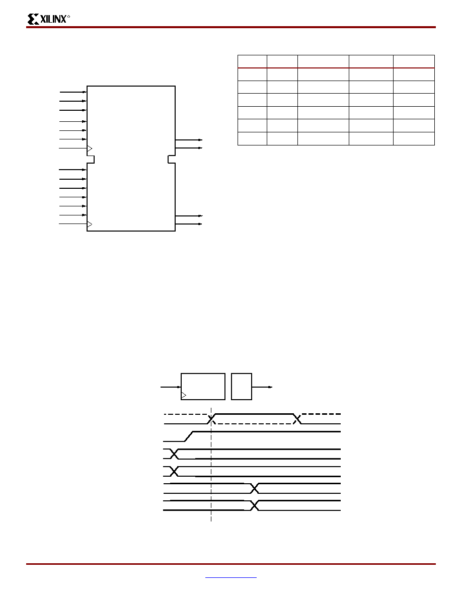
VirtexTM-II Platform FPGAs: Detailed Description
R
DS031-2 (v3.1) October 14, 2003
www.xilinx.com
Module 2 of 4
Product Specification
1-800-255-7778
23
Each block SelectRAM cell is a fully synchronous memory,
as illustrated in
Figure 30
. The two ports have independent
inputs and outputs and are independently clocked.
Port Aspect Ratios
Table 15
shows the depth and the width aspect ratios for the
18 Kbit block SelectRAM. Virtex-II block SelectRAM also
includes dedicated routing resources to provide an efficient
interface with CLBs, block SelectRAM, and multipliers.
Read/Write Operations
The Virtex-II block SelectRAM read operation is fully syn-
chronous. An address is presented, and the read operation
is enabled by control signals WEA and WEB in addition to
ENA or ENB. Then, depending on clock polarity, a rising or
falling clock edge causes the stored data to be loaded into
output registers.
The write operation is also fully synchronous. Data and
address are presented, and the write operation is enabled
by control signals WEA or WEB in addition to ENA or ENB.
Then, again depending on the clock input mode, a rising or
falling clock edge causes the data to be loaded into the
memory cell addressed.
A write operation performs a simultaneous read operation.
Three different options are available, selected by configura-
tion:
1.
"WRITE_FIRST"
The "WRITE_FIRST" option is a transparent mode. The
same clock edge that writes the data input (DI) into the
memory also transfers DI into the output registers DO
as shown in
Figure 31
.
Figure 30: 18 Kbit Block SelectRAM in Dual-Port Mode
DOPA
DOPB
DIPA
ADDRA
WEA
ENA
SSRA
CLKA
DIPB
ADDRB
WEB
ENB
SSRB
CLKB
18 Kbit Block SelectRAM
DS031_11_071602
DOB
DOA
DIA
DIB
Table 15: 18 Kbit Block SelectRAM Port Aspect Ratio
Width
Depth
Address Bus
Data Bus
Parity Bus
1
16,384
ADDR[13:0]
DATA[0]
N/A
2
8,192
ADDR[12:0]
DATA[1:0]
N/A
4
4,096
ADDR[11:0]
DATA[3:0]
N/A
9
2,048
ADDR[10:0]
DATA[7:0] Parity[0]
18
1,024
ADDR[9:0]
DATA[15:0] Parity[1:0]
36
512
ADDR[8:0]
DATA[31:0]
Parity[3:0]
Figure 31: WRITE_FIRST Mode
CLK
WE
Data_in
Data_in
New
aa
Address
Internal
Memory
DO
Data_out = Data_in
Data_out
DI
DS031_14_102000
New
RAM Contents
New
Old
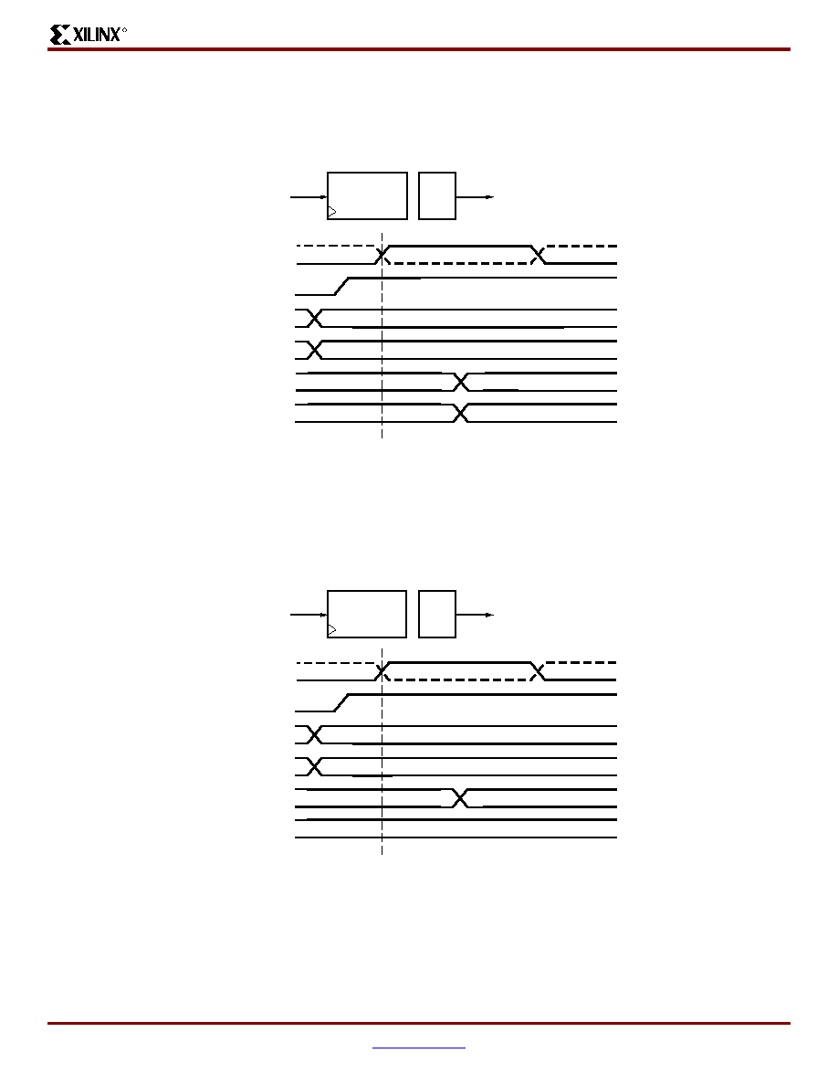
VirtexTM-II Platform FPGAs: Detailed Description
R
DS031-2 (v3.1) October 14, 2003
www.xilinx.com
Module 2 of 4
Product Specification
1-800-255-7778
24
2.
"READ_FIRST"
The "READ_FIRST" option is a read-before-write mode.
The same clock edge that writes data input (DI) into the memory also transfers the prior content of the memory cell
addressed into the data output registers DO, as shown in
Figure 32
.
3.
"NO_CHANGE"
The "NO_CHANGE" option maintains the content of the output registers, regardless of the write operation. The clock edge
during the write mode has no effect on the content of the data output register DO. When the port is configured as
"NO_CHANGE", only a read operation loads a new value in the output register DO, as shown in
Figure 33
.
Figure 32: READ_FIRST Mode
CLK
WE
Data_in
Data_in
New
aa
Old
Address
Internal
Memory
DO
Prior stored data
Data_out
DI
DS031_13_102000
RAM Contents
New
Old
Figure 33: NO_CHANGE Mode
CLK
WE
Data_in
Data_in
New
aa
Last Read Cycle Content (no change)
Address
Internal
Memory
DO
No change during write
Data_out
DI
DS031_12_102000
RAM Contents
New
Old

VirtexTM-II Platform FPGAs: Detailed Description
R
DS031-2 (v3.1) October 14, 2003
www.xilinx.com
Module 2 of 4
Product Specification
1-800-255-7778
25
Control Pins and Attributes
Virtex-II SelectRAM memory has two independent ports
with the control signals described in
Table 16
. All control
inputs including the clock have an optional inversion.
Initial memory content is determined by the INIT_xx
attributes. Separate attributes determine the output register
value after device configuration (INIT) and SSR is asserted
(SRVAL). Both attributes (INIT_B and SRVAL) are available
for each port when a block SelectRAM resource is config-
ured as dual-port RAM.
Locations
Virtex-II SelectRAM memory blocks are located in either
four or six columns. The number of blocks per column
depends of the device array size and is equivalent to the
number of CLBs in a column divided by four. Column loca-
tions are shown in
Table 17
.
Table 16: Control Functions
Control Signal
Function
CLK
Read and Write Clock
EN
Enable affects Read, Write, Set, Reset
WE
Write Enable
SSR
Set DO register to SRVAL (attribute)
Table 17: SelectRAM Memory Floor Plan
Device
Columns
SelectRAM Blocks
Per Column
Total
XC2V40
2
2
4
XC2V80
2
4
8
XC2V250
4
6
24
XC2V500
4
8
32
XC2V1000
4
10
40
XC2V1500
4
12
48
XC2V2000
4
14
56
XC2V3000
6
16
96
XC2V4000
6
20
120
XC2V6000
6
24
144
XC2V8000
6
28
168
Figure 34: Block SelectRAM (2-column, 4-column, and 6-column)
2 CLB columns
2 CLB columns
2 CLB columns
n CLB columns
2 CLB columns
n CLB columns
2 CLB columns
2 CLB columns
2 CLB columns
n CLB columns
n CLB columns
n CLB columns
2 CLB columns
n CLB columns
SelectRAM Blocks
SelectRAM Blocks
ds031_38_101000
2 CLB column
2 CLB columns
SelectRAM Blocks
2 CLB column
2 CLB columns
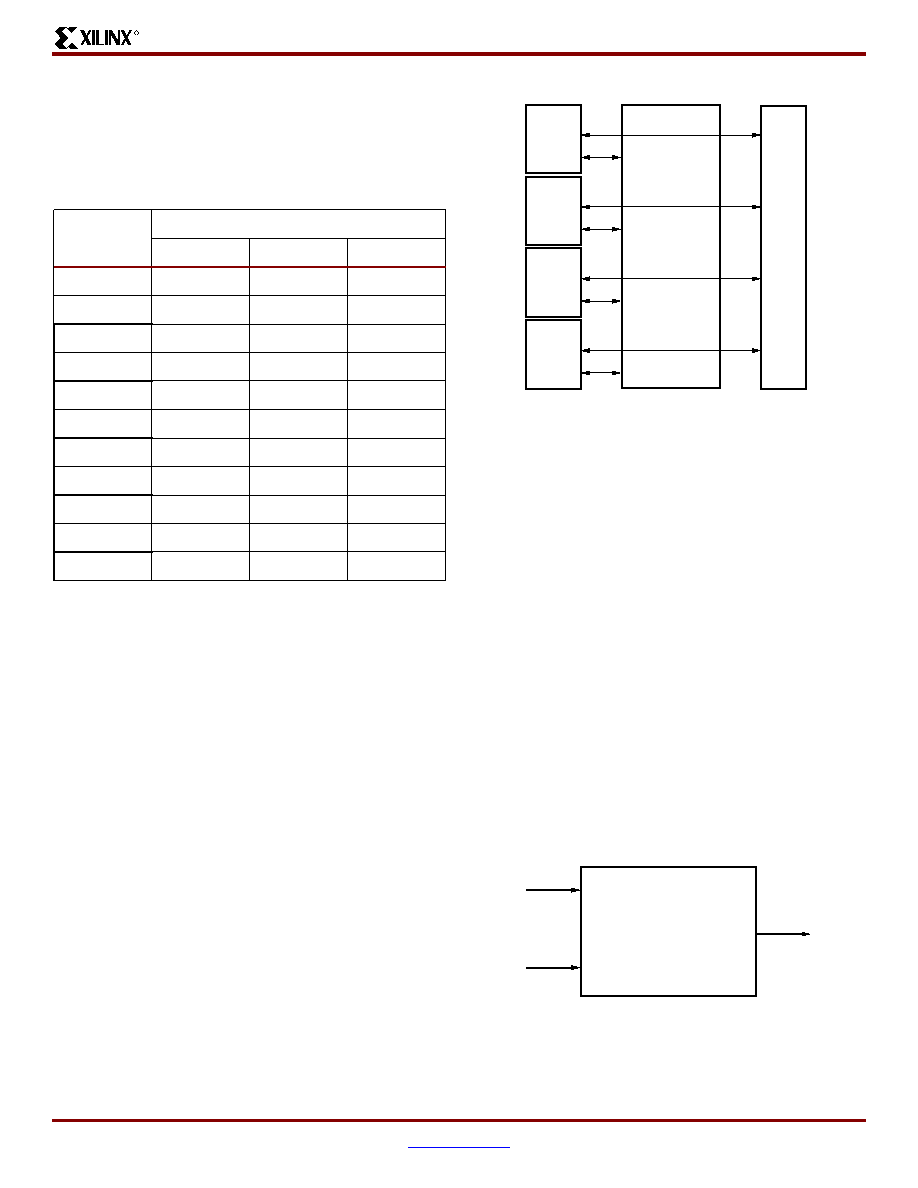
VirtexTM-II Platform FPGAs: Detailed Description
R
DS031-2 (v3.1) October 14, 2003
www.xilinx.com
Module 2 of 4
Product Specification
1-800-255-7778
26
Total Amount of SelectRAM Memory
Table 18
shows the amount of block SelectRAM memory
available for each Virtex-II device. The 18 Kbit SelectRAM
blocks are cascadable to implement deeper or wider single- or
dual-port memory resources.
18-Bit x 18-Bit Multipliers
Introduction
A Virtex-II multiplier block is an 18-bit by 18-bit 2's comple-
ment signed multiplier. Virtex-II devices incorporate many
embedded multiplier blocks. These multipliers can be asso-
ciated with an 18 Kbit block SelectRAM resource or can be
used independently. They are optimized for high-speed
operations and have a lower power consumption compared
to an 18-bit x 18-bit multiplier in slices.
Each SelectRAM memory and multiplier block is tied to four
switch matrices, as shown in
Figure 35
.
Association With Block SelectRAM Memory
The interconnect is designed to allow SelectRAM memory
and multiplier blocks to be used at the same time, but some
interconnect is shared between the SelectRAM and the
multiplier. Thus, SelectRAM memory can be used only up to
18 bits wide when the multiplier is used, because the multi-
plier shares inputs with the upper data bits of the
SelectRAM memory.
This sharing of the interconnect is optimized for an
18-bit-wide block SelectRAM resource feeding the multi-
plier. The use of SelectRAM memory and the multiplier with
an accumulator in LUTs allows for implementation of a digi-
tal signal processor (DSP) multiplier-accumulator (MAC)
function, which is commonly used in finite and infinite
impulse response (FIR and IIR) digital filters.
Configuration
The multiplier block is an 18-bit by 18-bit signed multiplier
(2's complement). Both A and B are 18-bit-wide inputs, and
the output is 36 bits.
Figure 36
shows a multiplier block.
Table 18: Virtex-II SelectRAM Memory Available
Device
Total SelectRAM Memory
Blocks
in Kbits
in Bits
XC2V40
4
72
73,728
XC2V80
8
144
147,456
XC2V250
24
432
442,368
XC2V500
32
576
589,824
XC2V1000
40
720
737,280
XC2V1500
48
864
884,736
XC2V2000
56
1,008
1,032,192
XC2V3000
96
1,728
1,769,472
XC2V4000
120
2,160
2,211,840
XC2V6000
144
2,592
2,654,208
XC2V8000
168
3,024
3,096,576
Figure 35: SelectRAM and Multiplier Blocks
Figure 36: Multiplier Block
Switch
Matrix
Switch
Matrix
18-Kbit block
SelectRAM
18 x 18 Multiplier
Switch
Matrix
Switch
Matrix
DS031_33_101000
MULT 18 x 18
A[17:0]
P[35:0]
B[17:0]
Multiplier Block
DS031_40_100400
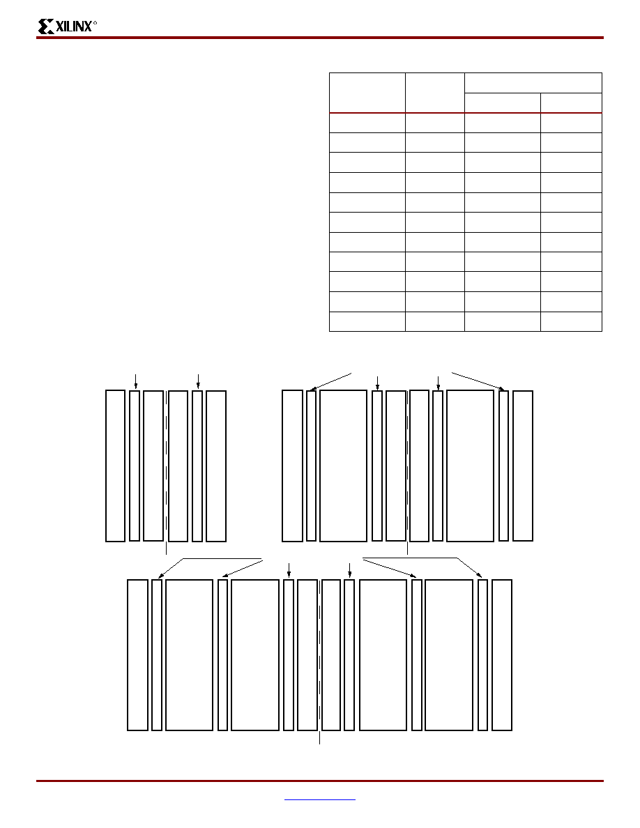
VirtexTM-II Platform FPGAs: Detailed Description
R
DS031-2 (v3.1) October 14, 2003
www.xilinx.com
Module 2 of 4
Product Specification
1-800-255-7778
27
Locations / Organization
Multiplier organization is identical to the 18 Kbit SelectRAM
organization, because each multiplier is associated with an
18 Kbit block SelectRAM resource.
In addition to the built-in multiplier blocks, the CLB elements
have dedicated logic to implement efficient multipliers in
logic. (Refer to
Configurable Logic Blocks (CLBs)
).
Table 19: Multiplier Floor Plan
Device
Columns
Multipliers
Per Column
Total
XC2V40
2
2
4
XC2V80
2
4
8
XC2V250
4
6
24
XC2V500
4
8
32
XC2V1000
4
10
40
XC2V1500
4
12
48
XC2V2000
4
14
56
XC2V3000
6
16
96
XC2V4000
6
20
120
XC2V6000
6
24
144
XC2V8000
6
28
168
Figure 37: Multipliers (2-column, 4-column, and 6-column)
DS031_39_101000
2 CLB columns
2 CLB columns
2 CLB columns
n CLB columns
2 CLB columns
n CLB columns
2 CLB columns
2 CLB columns
2 CLB columns
n CLB columns
n CLB columns
n CLB columns
2 CLB columns
n CLB columns
Multiplier Blocks
Multiplier Blocks
2 CLB column
2 CLB columns
Multiplier Blocks
2 CLB column
2 CLB columns
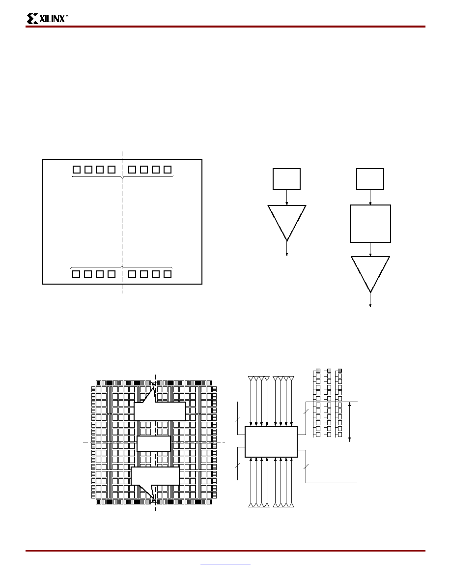
VirtexTM-II Platform FPGAs: Detailed Description
R
DS031-2 (v3.1) October 14, 2003
www.xilinx.com
Module 2 of 4
Product Specification
1-800-255-7778
28
Global Clock Multiplexer Buffers
Virtex-II devices have 16 clock input pins that can also be
used as regular user I/Os. Eight clock pads are on the top
edge of the device, in the middle of the array, and eight are
on the bottom edge, as illustrated in
Figure 38
.
The global clock multiplexer buffer represents the input to
dedicated low-skew clock tree distribution in Virtex-II
devices. Like the clock pads, eight global clock multiplexer
buffers are on the top edge of the device and eight are on
the bottom edge.
Each global clock buffer can either be driven by the clock
pad to distribute a clock directly to the device, or driven by
the Digital Clock Manager (DCM), discussed in
Digital
Clock Manager (DCM), page 30
. Each global clock buffer
can also be driven by local interconnects. The DCM has
clock output(s) that can be connected to global clock buffer
inputs, as shown in
Figure 39
.
Global clock buffers are used to distribute the clock to some
or all synchronous logic elements (such as registers in
CLBs and IOBs, and SelectRAM blocks.
Eight global clocks can be used in each quadrant of the
Virtex-II device. Designers should consider the clock distri-
bution detail of the device prior to pin-locking and floorplan-
ning (see the Virtex-II User Guide).
Figure 40
shows clock distribution in Virtex-II devices.
Figure 38: Virtex-II Clock Pads
8 clock pads
8 clock pads
Virtex-II
Device
DS031_42_101000
Figure 39: Virtex-II Clock Distribution Configurations
Clock
Pad
Clock
Buffer
I
0
Clock Distribution
Clock
Pad
Clock
Buffer
I
0
Clock Distribution
CLKIN
CLKOUT
DCM
DS031_43_101000
Figure 40: Virtex-II Clock Distribution
8
8
8
8
NW
NW
NE
SW
SE
NE
SW
SE
DS031_45_120200
8 BUFGMUX
8 BUFGMUX
8 max
8 BUFGMUX
8 BUFGMUX
16 Clocks
16 Clocks
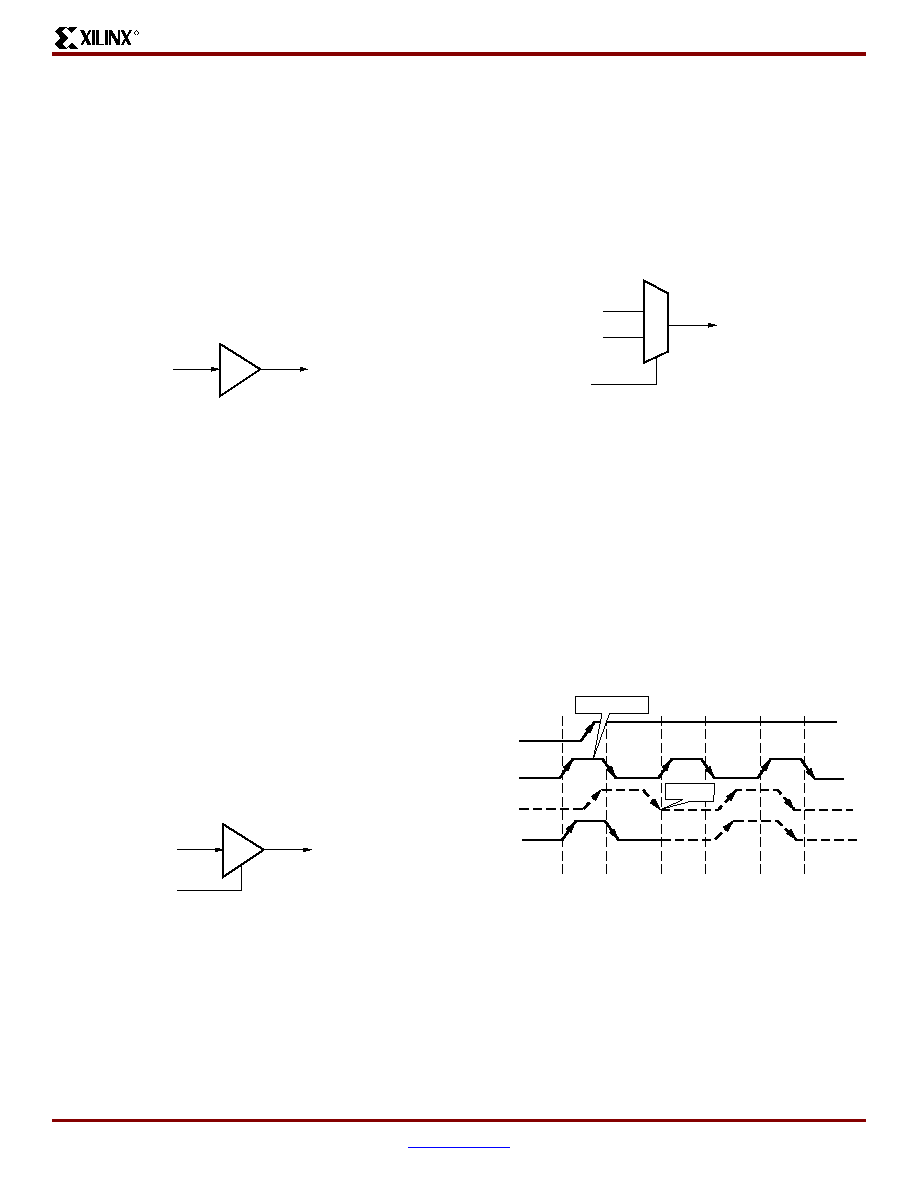
VirtexTM-II Platform FPGAs: Detailed Description
R
DS031-2 (v3.1) October 14, 2003
www.xilinx.com
Module 2 of 4
Product Specification
1-800-255-7778
29
In each quadrant, up to eight clocks are organized in clock
rows. A clock row supports up to 16 CLB rows (eight up and
eight down). For the largest devices a new clock row is
added, as necessary.
To reduce power consumption, any unused clock branches
remain static.
Global clocks are driven by dedicated clock buffers (BUFG),
which can also be used to gate the clock (BUFGCE) or to mul-
tiplex between two independent clock inputs (BUFGMUX).
The most common configuration option of this element is as
a buffer. A BUFG function in this (global buffer) mode, is
shown in
Figure 41
.
The Virtex-II global clock buffer BUFG can also be config-
ured as a clock enable/disable circuit (
Figure 42
), as well as
a two-input clock multiplexer (
Figure 43
). A functional
description of these two options is provided below. Each of
them can be used in either of two modes, selected by con-
figuration: rising clock edge or falling clock edge.
This section describes the rising clock edge option. For the
opposite option, falling clock edge, just change all "rising"
references to "falling" and all "High" references to "Low",
except for the description of the CE or S levels. The rising
clock edge option uses the BUFGCE and BUFGMUX prim-
itives. The falling clock edge option uses the BUFGCE_1
and BUFGMUX_1 primitives.
BUFGCE
If the CE input is active (High) prior to the incoming rising
clock edge, this Low-to-High-to-Low clock pulse passes
through the clock buffer. Any level change of CE during the
incoming clock High time has no effect.
If the CE input is inactive (Low) prior to the incoming rising
clock edge, the following clock pulse does not pass through
the clock buffer, and the output stays Low. Any level change
of CE during the incoming clock High time has no effect. CE
must not change during a short setup window just prior to
the rising clock edge on the BUFGCE input I. Violating this
setup time requirement can result in an undefined runt
pulse output.
BUFGMUX
BUFGMUX can switch between two unrelated, even asyn-
chronous clocks. Basically, a Low on S selects the I0 input,
a High on S selects the I1 input. Switching from one clock to
the other is done in such a way that the output High and Low
time is never shorter than the shortest High or Low time of
either input clock. As long as the presently selected clock is
High, any level change of S has no effect .
If the presently selected clock is Low while S changes, or if
it goes Low after S has changed, the output is kept Low until
the other ("to-be-selected") clock has made a transition
from High to Low. At that instant, the new clock starts driv-
ing the output.
The two clock inputs can be asynchronous with regard to
each other, and the S input can change at any time, except
for a short setup time prior to the rising edge of the presently
selected clock; that is, prior to the rising edge of the
BUFGMUX output O. Violating this setup time requirement
can result in an undefined runt pulse output.
All Virtex-II devices have 16 global clock multiplexer buffers.
Figure 44
shows a switchover from CLK0 to CLK1.
∑
The current clock is CLK0.
∑
S is activated High.
∑
If CLK0 is currently High, the multiplexer waits for CLK0
to go Low.
∑
Once CLK0 is Low, the multiplexer output stays Low
until CLK1 transitions High to Low.
∑
When CLK1 transitions from High to Low, the output
switches to CLK1.
∑
No glitches or short pulses can appear on the output.
Figure 41: Virtex-II BUFG Function
Figure 42: Virtex-II BUFGCE Function
O
I
BUFG
DS031_61_101200
O
I
CE
BUFGCE
DS031_62_101200
Figure 43: Virtex-II BUFGMUX Function
Figure 44: Clock Multiplexer Waveform Diagram
O
I0
I1
S
BUFGMUX
DS031_63_112900
S
CLK0
CLK1
OUT
Wait for Low
Switch
DS031_46_112900
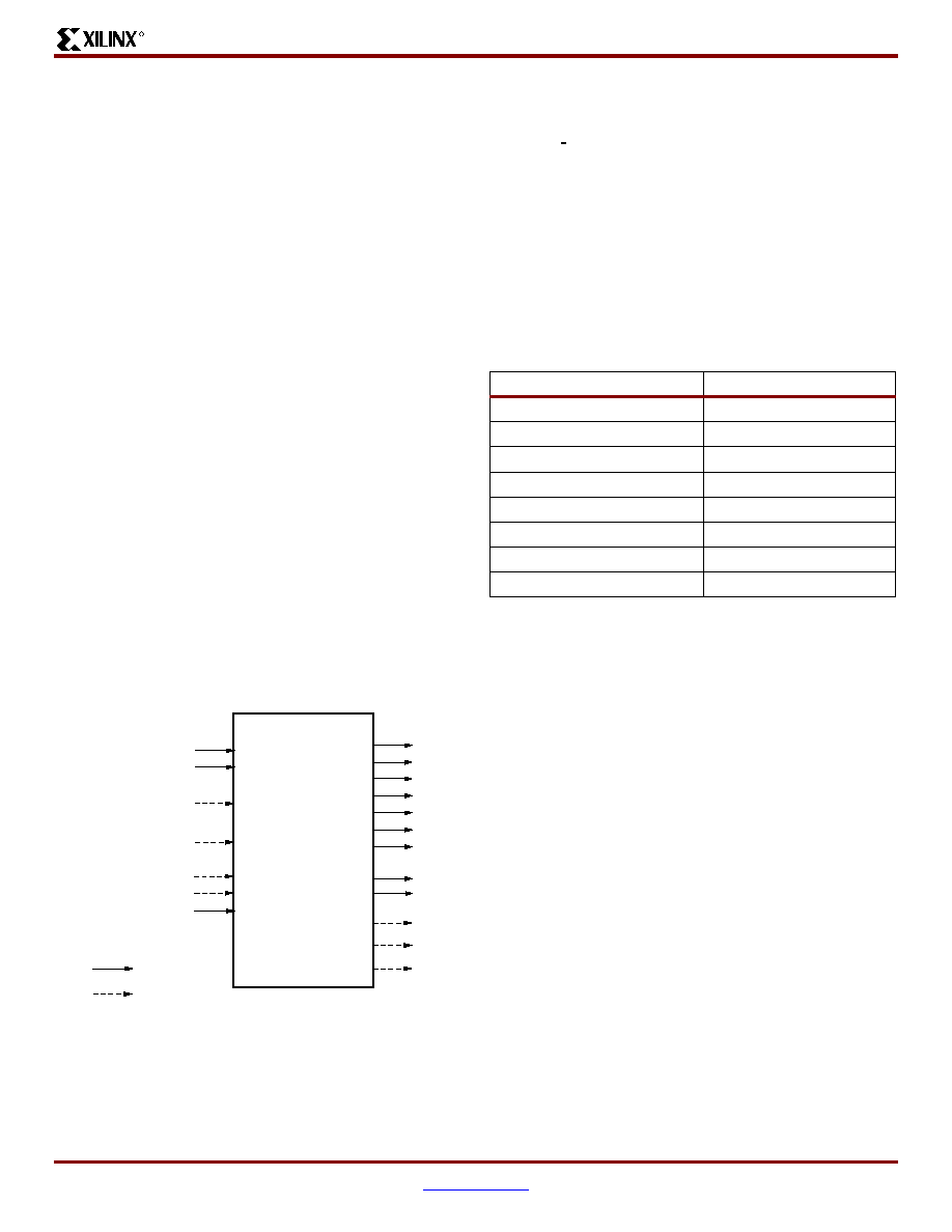
VirtexTM-II Platform FPGAs: Detailed Description
R
DS031-2 (v3.1) October 14, 2003
www.xilinx.com
Module 2 of 4
Product Specification
1-800-255-7778
30
Local Clocking
In addition to global clocks, there are local clock resources
in the Virtex-II devices. There are more than 72 local clocks
in the Virtex-II family. These resources can be used for
many different applications, including but not limited to
memory interfaces. For example, even using only the left
and right I/O banks, Virtex-II FPGAs can support up to 50
local clocks for DDR SDRAM. These interfaces can operate
beyond 200 MHz on Virtex-II devices.
Digital Clock Manager (DCM)
The Virtex-II DCM offers a wide range of powerful clock
management features.
∑
Clock De-skew: The DCM generates new system
clocks (either internally or externally to the FPGA),
which are phase-aligned to the input clock, thus
eliminating clock distribution delays.
∑
Frequency Synthesis: The DCM generates a wide
range of output clock frequencies, performing very
flexible clock multiplication and division.
∑
Phase Shifting: The DCM provides both coarse phase
shifting and fine-grained phase shifting with dynamic
phase shift control.
The DCM utilizes fully digital delay lines allowing robust
high-precision control of clock phase and frequency. It also
utilizes fully digital feedback systems, operating dynamically
to compensate for temperature and voltage variations dur-
ing operation.
Up to four of the nine DCM clock outputs can drive inputs to
global clock buffers or global clock multiplexer buffers simul-
taneously (see
Figure 45
). All DCM clock outputs can simul-
taneously drive general routing resources, including routes
to output buffers.
The DCM can be configured to delay the completion of the
Virtex-II configuration process until after the DCM has
achieved lock. This guarantees that the chip does not begin
operating until after the system clocks generated by the
DCM have stabilized.
The DCM has the following general control signals:
∑
RST input pin
:
resets the entire DCM
∑
LOCKED output pin: asserted High when all enabled
DCM circuits have locked.
∑
STATUS output pins (active High): shown in
Table 20
.
Clock De-Skew
The DCM de-skews the output clocks relative to the input
clock by automatically adjusting a digital delay line. Addi-
tional delay is introduced so that clock edges arrive at inter-
nal registers and block RAMs simultaneously with the clock
edges arriving at the input clock pad. Alternatively, external
clocks, which are also de-skewed relative to the input clock,
can be generated for board-level routing. All DCM output
clocks are phase-aligned to CLK0 and, therefore, are also
phase-aligned to the input clock.
To achieve clock de-skew, the CLKFB input must be con-
nected, and its source must be either CLK0 or CLK2X. Note
that CLKFB must always be connected, unless only the CLKFX
or CLKFX180 outputs are used and de-skew is not required.
Frequency Synthesis
The DCM provides flexible methods for generating new
clock frequencies. Each method has a different operating
frequency range and different AC characteristics. The
CLK2X and CLK2X180 outputs double the clock frequency.
The CLKDV output creates divided output clocks with divi-
sion options of 1.5, 2, 2.5, 3, 3.5, 4, 4.5, 5, 5.5, 6, 6.5, 7, 7.5,
8, 9, 10, 11, 12, 13, 14, 15, and 16.
The CLKFX and CLKFX180 outputs can be used to pro-
duce clocks at the following frequency:
FREQ
CLKFX
= (M/D) * FREQ
CLKIN
Figure 45: Digital Clock Manager
CLKIN
CLKFB
CLK180
CLK270
CLK0
CLK90
CLK2X
CLK2X180
CLKDV
DCM
DS031_67_112900
CLKFX
CLKFX180
LOCKED
STATUS[7:0]
PSDONE
RST
DSSEN
PSINCDEC
PSEN
PSCLK
clock signal
control signal
Table 20: DCM Status Pins
Status Pin
Function
0
Phase Shift Overflow
1
CLKIN Stopped
2
CLKFX Stopped
3
N/A
4
N/A
5
N/A
6
N/A
7
N/A
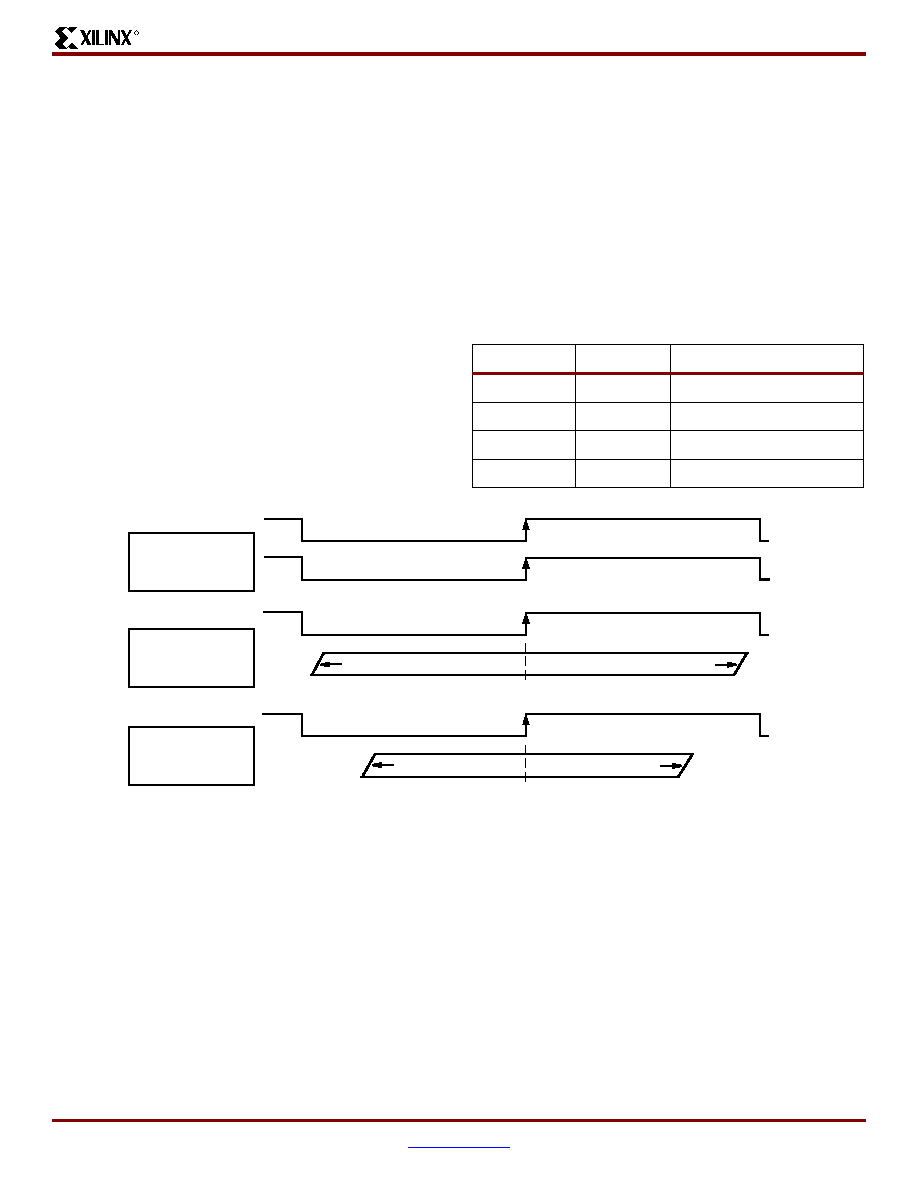
VirtexTM-II Platform FPGAs: Detailed Description
R
DS031-2 (v3.1) October 14, 2003
www.xilinx.com
Module 2 of 4
Product Specification
1-800-255-7778
31
where M and D are two integers. Specifications for M and D
are provided under
DCM Timing Parameters
in Module 3.
By default, M=4 and D=1, which results in a clock output fre-
quency four times faster than the clock input frequency
(CLKIN).
CLK2X180 is phase shifted 180 degrees relative to CLK2X.
CLKFX180 is phase shifted 180 degrees relative to CLKFX.
All frequency synthesis outputs automatically have 50/50
duty cycles (with the exception of the CLKDV output when
performing a non-integer divide in high-frequency mode).
Note that CLK2X and CLK2X180 are not available in
high-frequency mode.
Phase Shifting
The DCM provides additional control over clock skew
through either coarse or fine-grained phase shifting. The
CLK0, CLK90, CLK180, and CLK270 outputs are each
phase shifted by º of the input clock period relative to each
other, providing coarse phase control. Note that CLK90 and
CLK270 are not available in high-frequency mode.
Fine-phase adjustment affects all nine DCM output clocks.
When activated, the phase shift between the rising edges of
CLKIN and CLKFB is a specified fraction of the input clock
period.
In variable mode, the
PHASE_SHIFT
value can also be
dynamically incremented or decremented as determined by
PSINCDEC synchronously to PSCLK, when the PSEN
input is active.
Figure 46
illustrates the effects of fine-phase
shifting. For more information on DCM features, see the
Virtex-II User Guide.
Table 21
lists fine-phase shifting control pins, when used in
variable mode.
Two separate components of the phase shift range must be
understood:
∑
PHASE_SHIFT
attribute range
∑
FINE_SHIFT_RANGE
DCM timing parameter range
The
PHASE_SHIFT
attribute is the numerator in the following
equation:
Phase Shift (ns) = (
PHASE_SHIFT
/256) * PERIOD
CLKIN
The full range of this attribute is always -255 to +255, but its
practical range varies with CLKIN frequency, as constrained
by the
FINE_SHIFT_RANGE
component, which represents
the total delay achievable by the phase shift delay line. Total
delay is a function of the number of delay taps used in the
circuit. Across process, voltage, and temperature, this abso-
lute range is guaranteed to be as specified under
DCM Tim-
ing Parameters
in Module 3.
Absolute range (fixed mode) = ±
FINE_SHIFT_RANGE
Absolute range (variable mode) = ±
FINE_SHIFT_RANGE
/2
The reason for the difference between fixed and variable
modes is as follows. For variable mode to allow symmetric,
dynamic sweeps from -255/256 to +255/256, the DCM sets
the "zero phase skew" point as the middle of the delay line,
thus dividing the total delay line range in half. In fixed mode,
since the
PHASE_SHIFT
value never changes after configu-
ration, the entire delay line is available for insertion into
either the CLKIN or CLKFB path (to create either positive or
negative skew).
Table 21: Fine-Phase Shifting Control Pins
Control Pin
Direction
Function
PSINCDEC
in
Increment or decrement
PSEN
in
Enable ± phase shift
PSCLK
in
Clock for phase shift
PSDONE
out
Active when completed
Figure 46: Fine-Phase Shifting Effects
CLKOUT_PHASE_SHIFT
= FIXED
CLKOUT_PHASE_SHIFT
= VARIABLE
CLKOUT_PHASE_SHIFT
= NONE
CLKIN
CLKIN
CLKIN
CLKFB
(PS/256) x PERIODCLKIN
(PS negative)
(PS/256) x PERIODCLKIN
(PS positive)
(PS/256) x PERIODCLKIN
(PS negative)
(PS/256) x PERIODCLKIN
(PS positive)
DS031_48_101201
CLKFB
CLKFB
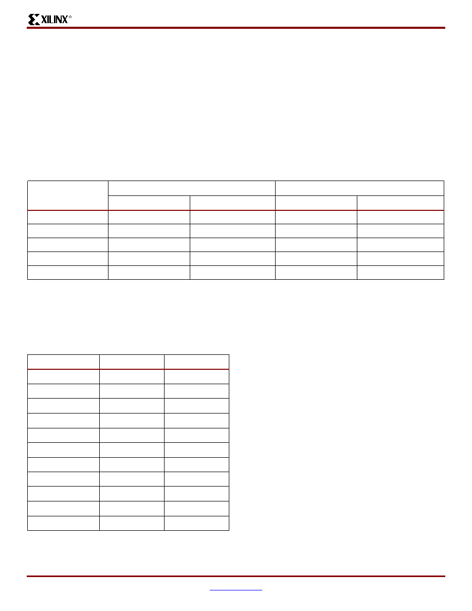
VirtexTM-II Platform FPGAs: Detailed Description
R
DS031-2 (v3.1) October 14, 2003
www.xilinx.com
Module 2 of 4
Product Specification
1-800-255-7778
32
Taking both of these components into consideration, the fol-
lowing are some usage examples:
∑
If PERIOD
CLKIN
= 2 *
FINE_SHIFT_RANGE
, then
PHASE_SHIFT in
fixed mode is limited to
±
128, and in
variable mode it is limited to
±
64.
∑
If PERIOD
CLKIN
=
FINE_SHIFT_RANGE
, then
PHASE_SHIFT in
fixed mode is limited to
±
255, and in
variable mode it is limited to
±
128.
∑
If PERIOD
CLKIN
0.5 *
FINE_SHIFT_RANGE
, then
PHASE_SHIFT
is limited to
±
255 in either mode.
Operating Modes
The frequency ranges of DCM input and output clocks
depend on the operating mode specified, either
low-frequency mode or high-frequency mode, according to
Table 22
. (For actual values, see
Virtex-II Switching Char-
acteristics
in Module 3). The CLK2X, CLK2X180, CLK90,
and CLK270 outputs are not available in high-frequency
mode.
High or low-frequency mode is selected by an attribute.
Locations/Organization
Virtex-II DCMs are placed on the top and bottom of each
block RAM and multiplier column. The number of DCMs
depends on the device size, as shown in
Table 23
.
Table 22: DCM Frequency Ranges
Output Clock
Low-Frequency Mode
High-Frequency Mode
CLKIN Input
CLK Output
CLKIN Input
CLK Output
CLK0, CLK180
CLKIN_FREQ_DLL_LF
CLKOUT_FREQ_1X_LF
CLKIN_FREQ_DLL_HF
CLKOUT_FREQ_1X_HF
CLK90, CLK270
CLKIN_FREQ_DLL_LF
CLKOUT_FREQ_1X_LF
NA
NA
CLK2X, CLK2X180
CLKIN_FREQ_DLL_LF
CLKOUT_FREQ_2X_LF
NA
NA
CLKDV
CLKIN_FREQ_DLL_LF
CLKOUT_FREQ_DV_LF
CLKIN_FREQ_DLL_HF
CLKOUT_FREQ_DV_HF
CLKFX, CLKFX180
CLKIN_FREQ_FX_LF
CLKOUT_FREQ_FX_LF
CLKIN_FREQ_FX_HF
CLKOUT_FREQ_FX_HF
Table 23: DCM Organization
Device
Columns
DCMs
XC2V40
2
4
XC2V80
2
4
XC2V250
4
8
XC2V500
4
8
XC2V1000
4
8
XC2V1500
4
8
XC2V2000
4
8
XC2V3000
6
12
XC2V4000
6
12
XC2V6000
6
12
XC2V8000
6
12
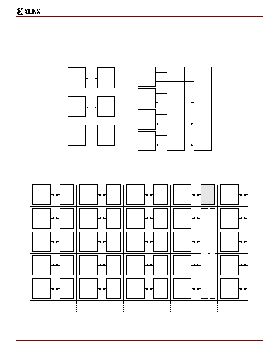
VirtexTM-II Platform FPGAs: Detailed Description
R
DS031-2 (v3.1) October 14, 2003
www.xilinx.com
Module 2 of 4
Product Specification
1-800-255-7778
33
Active Interconnect Technology
Local and global Virtex-II routing resources are optimized for speed and timing predictability, as well as to facilitate IP cores
implementation. Virtex-II Active Interconnect Technology is a fully buffered programmable routing matrix. All routing
resources are segmented to offer the advantages of a hierarchical solution. Virtex-II logic features like CLBs, IOBs, block
RAM, multipliers, and DCMs are all connected to an identical switch matrix for access to global routing resources, as shown
in
Figure 47
.
Each Virtex-II device can be represented as an array of switch matrixes with logic blocks attached, as illustrated in
Figure 48
.
Figure 47: Active Interconnect Technology
Figure 48: Routing Resources
Switch
Matrix
Switch
Matrix
Switch
Matrix
Switch
Matrix
Switch
Matrix
CLB
18Kb
BRAM
MULT
18 x 18
Switch
Matrix
IOB
Switch
Matrix
DCM
DS031_55_101000
Switch
Matrix
IOB
Switch
Matrix
IOB
Switch
Matrix
IOB
Switch
Matrix
DCM
Switch
Matrix
Switch
Matrix
IOB
Switch
Matrix
CLB
Switch
Matrix
CLB
Switch
Matrix
Switch
Matrix
Switch
Matrix
IOB
Switch
Matrix
CLB
Switch
Matrix
CLB
Switch
Matrix
Switch
Matrix
Switch
Matrix
IOB
Switch
Matrix
CLB
Switch
Matrix
CLB
Switch
Matrix
Switch
Matrix
Switch
Matrix
IOB
Switch
Matrix
CLB
Switch
Matrix
CLB
Switch
Matrix
Switch
Matrix
SelectRAM
Multiplier
DS031_34_110300
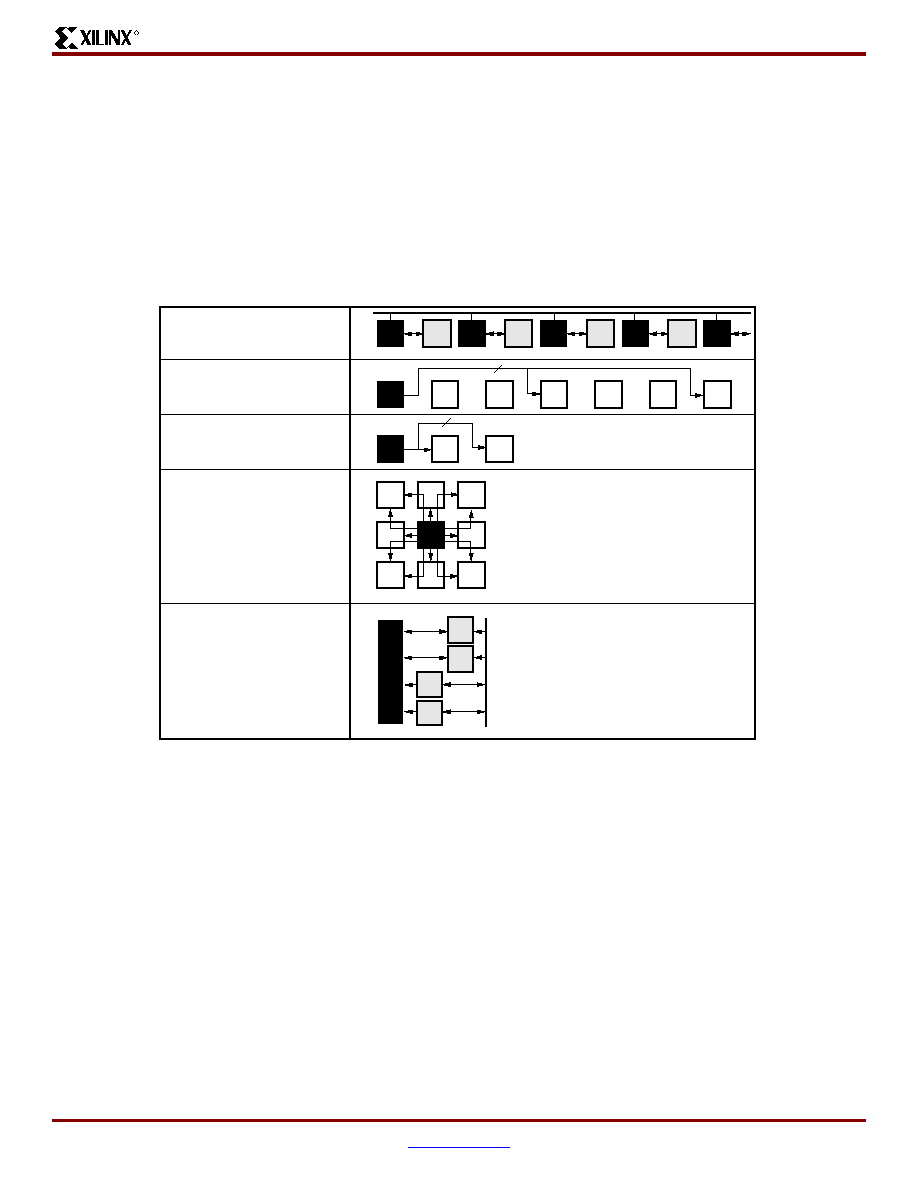
VirtexTM-II Platform FPGAs: Detailed Description
R
DS031-2 (v3.1) October 14, 2003
www.xilinx.com
Module 2 of 4
Product Specification
1-800-255-7778
34
Place-and-route software takes advantage of this regular
array to deliver optimum system performance and fast com-
pile times. The segmented routing resources are essential
to guarantee IP cores portability and to efficiently handle an
incremental design flow that is based on modular imple-
mentations. Total design time is reduced due to fewer and
shorter design iterations.
Hierarchical Routing Resources
Most Virtex-II signals are routed using the global routing
resources, which are located in horizontal and vertical rout-
ing channels between each switch matrix.
As shown in
Figure 49
, Virtex-II has fully buffered program-
mable interconnections, with a number of resources
counted between any two adjacent switch matrix rows or
columns. Fanout has minimal impact on the performance of
each net.
∑
The long lines are bidirectional wires that distribute
signals across the device. Vertical and horizontal long
lines span the full height and width of the device.
∑
The hex lines route signals to every third or sixth block
away in all four directions. Organized in a staggered
pattern, hex lines can only be driven from one end.
Hex-line signals can be accessed either at the endpoints
or at the midpoint (three blocks from the source).
∑
The double lines route signals to every first or second
block away in all four directions. Organized in a
staggered pattern, double lines can be driven only at
their endpoints. Double-line signals can be accessed
either at the endpoints or at the midpoint (one block
from the source).
∑
The direct connect lines route signals to neighboring
blocks: vertically, horizontally, and diagonally.
∑
The fast connect lines are the internal CLB local
interconnections from LUT outputs to LUT inputs.
Dedicated Routing
In addition to the global and local routing resources, dedi-
cated signals are available.
∑
There are eight global clock nets per quadrant (see
Global Clock Multiplexer Buffers
).
∑
Horizontal routing resources are provided for on-chip
3-state busses. Four partitionable bus lines are
provided per CLB row, permitting multiple busses
within a row. (See
3-State Buffers
.)
∑
Two dedicated carry-chain resources per slice column
(two per CLB column) propagate carry-chain MUXCY
output signals vertically to the adjacent slice. (See
CLB/Slice Configurations
.)
Figure 49: Hierarchical Routing Resources
24 Horizontal Long Lines
24 Vertical Long Lines
120 Horizontal Hex Lines
120 Vertical Hex Lines
40 Horizontal Double Lines
40 Vertical Double Lines
16 Direct Connections
(total in all four directions)
8 Fast Connects
DS031_60_110200

VirtexTM-II Platform FPGAs: Detailed Description
R
DS031-2 (v3.1) October 14, 2003
www.xilinx.com
Module 2 of 4
Product Specification
1-800-255-7778
35
∑
One dedicated SOP chain per slice row (two per CLB
row) propagate ORCY output logic signals horizontally
to the adjacent slice. (See
Sum of Products
.)
∑
One dedicated shift-chain per CLB connects the output
of LUTs in shift-register mode to the input of the next
LUT in shift-register mode (vertically) inside the CLB.
(See
Shift Registers, page 16
.)
Creating a Design
Creating Virtex-II designs is easy with Xilinx Integrated Syn-
thesis Environment (ISE) development systems, which sup-
port advanced design capabilities, including ProActive
Timing Closure, integrated logic analysis, and the fastest
place and route runtimes in the industry. ISE solutions
enable designers to get the performance they need, quickly
and easily.
As a result of the ongoing cooperative development efforts
between Xilinx and EDA Alliance partners, designers can
take advantage of the benefits provided by EDA technolo-
gies in the programmable logic design process. Xilinx devel-
opment systems are available in a number of easy to use
configurations, collectively known as the ISE Series.
ISE Alliance
The ISE Alliance solution is designed to plug and play within
an existing design environment. Built using industry standard
data formats and netlists, these stable, flexible products
enable Alliance EDA partners to deliver their best design
automation capabilities to Xilinx customers, along with the
time to market benefits of ProActive Timing Closure.
ISE Foundation
The ISE Foundation solution delivers the benefits of true
HDL-based design in a seamlessly integrated design envi-
ronment. An intuitive project navigator, as well as powerful
HDL design and two HDL synthesis tools, ensure that
high-quality results are achieved quickly and easily. The ISE
Foundation product includes:
∑
State Diagram entry using Xilinx StateCAD
∑
Automatic HDL Testbench generation using Xilinx
HDLBencher
∑
HDL Simulation using ModelSim XE
Design Flow
Virtex-II design flow proceeds as follows:
∑
Design Entry
∑
Synthesis
∑
Implementation
∑
Verification
Most programmable logic designers iterate through these
steps several times in the process of completing a design.
Design Entry
All Xilinx ISE development systems support the mainstream
EDA design entry capabilities, ranging from schematic
design to advanced HDL design methodologies. Given the
high densities of the Virtex-II family, designs are created
most efficiently using HDLs. To further improve their time to
market, many Xilinx customers employ incremental, modu-
lar, and Intellectual Property (IP) design techniques. When
properly used, these techniques further accelerate the logic
design process.
To enable designers to leverage existing investments in
EDA tools, and to ensure high performance design flows,
Xilinx jointly develops tools with leading EDA vendors,
including:
∑
Aldec
Æ
∑
Cadence
Æ
∑
Exemplar
Æ
∑
Mentor Graphics
Æ
∑
Model Technology
Æ
∑
Synopsys
Æ
∑
Synplicity
Æ
Complete information on Alliance Series partners and their
associated design flows is available at
www.xilinx.com
on
the Xilinx Alliance Series web page.
The ISE Foundation product offers schematic entry and
HDL design capabilities as part of an integrated design
solution - enabling one-stop shopping. These capabilities
are powerful, easy to use, and they support the full portfolio
of Xilinx programmable logic devices. HDL design capabil-
ities include a color-coded HDL editor with integrated lan-
guage templates, state diagram entry, and Core generation
capabilities.
Synthesis
The ISE Alliance product is engineered to support
advanced design flows with the industry's best synthesis
tools. Advanced design methodologies include:
∑
Physical Synthesis
∑
Incremental synthesis
∑
RTL floorplanning
∑
Direct physical mapping
The ISE Foundation product seamlessly integrates synthesis
capabilities purchased directly from Exemplar, Synopsys, and
Synplicity. In addition, it includes the capabilities of Xilinx
Synthesis Technology.
A benefit of having two seamlessly integrated synthesis
engines within an ISE design flow is the ability to apply alter-
native sets of optimization techniques on designs, helping to
ensure that designers can meet even the toughest timing
requirements.

VirtexTM-II Platform FPGAs: Detailed Description
R
DS031-2 (v3.1) October 14, 2003
www.xilinx.com
Module 2 of 4
Product Specification
1-800-255-7778
36
Design Implementation
The ISE Series development systems include Xilinx tim-
ing-driven implementation tools, frequently called "place
and route" or "fitting" software. This robust suite of tools
enables the creation of an intuitive, flexible, tightly inte-
grated design flow that efficiently bridges "logical" and
"physical" design domains. This simplifies the task of defin-
ing a design, including its behavior, timing requirements,
and optional layout (or floorplanning), as well as simplifying
the task of analyzing reports generated during the imple-
mentation process.
The Virtex-II implementation process is comprised of Syn-
thesis, translation, mapping, place and route, and configu-
ration file generation. While the tools can be run individually,
many designers choose to run the entire implementation
process with the click of a button. To assist those who prefer
to script their design flows, Xilinx provides Xflow, an auto-
mated single command line process.
Design Verification
In addition to conventional design verification using static
timing analysis or simulation techniques, Xilinx offers pow-
erful in-circuit debugging techniques using ChipScope ILA
(Integrated Logic Analysis). The reconfigurable nature of
Xilinx FPGAs means that designs can be verified in real
time without the need for extensive sets of software simula-
tion vectors.
For simulation, the system extracts post-layout timing infor-
mation from the design database, and back-annotates this
information into the netlist for use by the simulator. The back
annotation features a variety of patented Xilinx techniques,
resulting in the industry's most powerful simulation flows.
Alternatively, timing-critical portions of a design can be ver-
ified using the Xilinx static timing analyzer or a third party
static timing analysis tool like Synopsys Prime TimeTM, by
exporting timing data in the STAMP data format.
For in-circuit debugging, ChipScope ILA enables designers
to analyze the real-time behavior of a device while operating
at full system speeds. Logic analysis commands and cap-
tured data are transferred between the ChipScope software
and ILA cores within the Virtex-II FPGA, using industry
standard JTAG protocols. These JTAG transactions are
driven over an optional download cable (MultiLINX or
JTAG), connecting the Virtex device in the target system to
a PC or workstation.
ChipScope ILA was designed to look and feel like a logic
analyzer, making it easy to begin debugging a design imme-
diately. Modifications to the desired logic analysis can be
downloaded directly into the system in a matter of minutes.
Other Unique Features of Virtex-II Design Flow
Xilinx design flows feature a number of unique capabilities.
Among these are efficient incremental HDL design flows; a
robust capability that is enabled by Xilinx exclusive hierar-
chical floorplanning capabilities. Another powerful design
capability only available in the Xilinx design flow is "Modular
Design", part of the Xilinx suite of team design tools, which
enables autonomous design, implementation, and verifica-
tion of design modules.
Incremental Synthesis
Xilinx unique hierarchical floorplanning capabilities enable
designers to create a programmable logic design by isolating
design changes within one hierarchical "logic block", and
perform synthesis, verification and implementation pro-
cesses on that specific logic block. By preserving the logic in
unchanged portions of a design, Xilinx incremental design
makes the high-density design process more efficient.
Xilinx hierarchical floorplanning capabilities can be speci-
fied using the high-level floorplanner or a preferred RTL
floorplanner (see the Xilinx web site for a list of supported
EDA partners). When used in conjunction with one of the
EDA partners' floorplanners, higher performance results
can be achieved, as many synthesis tools use this more
predictable detailed physical implementation information to
establish more aggressive and accurate timing estimates
when performing their logic optimizations.
Modular Design
Xilinx innovative modular design capabilities take the incre-
mental design process one step further by enabling the
designer to delegate responsibility for completing the
design, synthesis, verification, and implementation of a hier-
archical "logic block" to an arbitrary number of designers -
assigning a specific region within the target FPGA for exclu-
sive use by each of the team members.
This team design capability enables an autonomous
approach to design modules, changing the hand-off point to
the lead designer or integrator from "my module works in
simulation" to "my module works in the FPGA". This unique
design methodology also leverages the Xilinx hierarchical
floorplanning capabilities and enables the Xilinx (or EDA
partner) floorplanner to manage the efficient implementa-
tion of very high-density FPGAs.
Configuration
Virtex-II devices are configured by loading application spe-
cific configuration data into the internal configuration mem-
ory. Configuration is carried out using a subset of the device
pins, some of which are dedicated, while others can be
re-used as general purpose inputs and outputs once config-
uration is complete.
Depending on the system design, several configuration
modes are supported, selectable via mode pins. The mode
pins M2, M1 and M0 are dedicated pins. An additional pin,
HSWAP_EN is used in conjunction with the mode pins to
select whether user I/O pins have pull-ups during configura-
tion. By default, HSWAP_EN is tied High (internal pull-up)
which shuts off the pull-ups on the user I/O pins during con-
figuration. When HSWAP_EN is tied Low, user I/Os have

VirtexTM-II Platform FPGAs: Detailed Description
R
DS031-2 (v3.1) October 14, 2003
www.xilinx.com
Module 2 of 4
Product Specification
1-800-255-7778
37
pull-ups during configuration. Other dedicated pins are
CCLK (the configuration clock pin), DONE, PROG_B, and
the boundary-scan pins: TDI, TDO, TMS, and TCK.
Depending on the configuration mode chosen, CCLK can
be an output generated by the FPGA, or an input accepting
an externally generated clock. The configuration pins and
boundary scan pins are independent of the V
CCO
. The aux-
iliary power supply (V
CCAUX
) of 3.3V is used for these pins.
All configuration pins are LVTTL 12 mA. (See
Virtex-II DC
Characteristics
in Module 3.)
A persist option is available which can be used to force the
configuration pins to retain their configuration function even
after device configuration is complete. If the persist option is
not selected then the configuration pins with the exception
of CCLK, PROG_B, and DONE can be used as user I/O in
normal operation. The persist option does not apply to the
boundary-scan related pins. The persist feature is valuable
in applications which employ partial reconfiguration or
reconfiguration on the fly.
Configuration Modes
Virtex-II supports the following five configuration modes:
∑
Slave-serial mode
∑
Master-serial mode
∑
Slave SelectMAP mode
∑
Master SelectMAP mode
∑
Boundary-Scan mode (IEEE 1532/IEEE 1149)
A detailed description of configuration modes is provided in
the Virtex-II User Guide.
Slave-Serial Mode
In slave-serial mode, the FPGA receives configuration data
in bit-serial form from a serial PROM or other serial source
of configuration data. The CCLK pin on the FPGA is an
input in this mode. The serial bitstream must be setup at the
DIN input pin a short time before each rising edge of the
externally generated CCLK.
Multiple FPGAs can be daisy-chained for configuration from
a single source. After a particular FPGA has been config-
ured, the data for the next device is routed internally to the
DOUT pin. The data on the DOUT pin changes on the falling
edge of CCLK.
Slave-serial mode is selected by applying <111> to the
mode pins (M2, M1, M0). A weak pull-up on the mode pins
makes slave serial the default mode if the pins are left
unconnected.
Master-Serial Mode
In master-serial mode, the CCLK pin is an output pin. It is
the Virtex-II FPGA device that drives the configuration clock
on the CCLK pin to a Xilinx Serial PROM which in turn feeds
bit-serial data to the DIN input. The FPGA accepts this data
on each rising CCLK edge. After the FPGA has been
loaded, the data for the next device in a daisy-chain is pre-
sented on the DOUT pin after the falling CCLK edge.
The interface is identical to slave serial except that an inter-
nal oscillator is used to generate the configuration clock
(CCLK). A wide range of frequencies can be selected for
CCLK which always starts at a slow default frequency. Con-
figuration bits then switch CCLK to a higher frequency for
the remainder of the configuration.
Slave SelectMAP Mode
The SelectMAP mode is the fastest configuration option.
Byte-wide data is written into the Virtex-II FPGA device with
a BUSY flag controlling the flow of data. An external data
source provides a byte stream, CCLK, an active Low Chip
Select (CS_B) signal and a Write signal (RDWR_B). If
BUSY is asserted (High) by the FPGA, the data must be
held until BUSY goes Low. Data can also be read using the
SelectMAP mode. If RDWR_B is asserted, configuration
data is read out of the FPGA as part of a readback opera-
tion.
After configuration, the pins of the SelectMAP port can be
used as additional user I/O. Alternatively, the port can be
retained to permit high-speed 8-bit readback using the per-
sist option.
Multiple Virtex-II FPGAs can be configured using the
SelectMAP mode, and be made to start-up simultaneously.
To configure multiple devices in this way, wire the individual
CCLK, Data, RDWR_B, and BUSY pins of all the devices in
parallel. The individual devices are loaded separately by
deasserting the CS_B pin of each device in turn and writing
the appropriate data.
Master SelectMAP Mode
This mode is a master version of the SelectMAP mode. The
device is configured byte-wide on a CCLK supplied by the
Virtex-II FPGA device. Timing is similar to the Slave Serial-
MAP mode except that CCLK is supplied by the Virtex-II
FPGA.
Boundary-Scan (JTAG, IEEE 1532) Mode
In boundary-scan mode, dedicated pins are used for config-
uring the Virtex-II device. The configuration is done entirely
through the IEEE 1149.1 Test Access Port (TAP). Virtex-II
device configuration using Boundary scan is compliant with
IEEE 1149.1-1993 standard and the new IEEE 1532 stan-
dard for In-System Configurable (ISC) devices. The IEEE
1532 standard is backward compliant with the IEEE
1149.1-1993 TAP and state machine. The IEEE Standard
1532 for In-System Configurable (ISC) devices is intended
to be programmed, reprogrammed, or tested on the board
via a physical and logical protocol.
Configuration through the boundary-scan port is always
available, independent of the mode selection. Selecting the
boundary-scan mode simply turns off the other modes.
VirtexTM-II Platform FPGAs: Detailed Description
R
DS031-2 (v3.1) October 14, 2003
www.xilinx.com
Module 2 of 4
Product Specification
1-800-255-7778
38
Table 25
lists the total number of bits required to configure
each device.
Configuration Sequence
The configuration of Virtex-II devices is a three-phase pro-
cess after Power On Reset or POR. POR occurs when
V
CCINT
is greater than 1.2V, V
CCAUX
is greater than 2.5V,
and V
CCO
(bank 4) is greater than 1.5V. Once the POR volt-
ages have been reached, the three-phase process begins.
First, the configuration memory is cleared. Next, con-
figuration data is loaded into the memory, and finally, the
logic is activated by a start-up process.
Configuration is automatically initiated on power-up unless
it is delayed by the user. The INIT_B pin can be held Low
using an open-drain driver. An open-drain is required since
INIT_B is a bidirectional open-drain pin that is held Low by a
Virtex-II FPGA device while the configuration memory is
being cleared. Extending the time that the pin is Low causes
the configuration sequencer to wait. Thus, configuration is
delayed by preventing entry into the phase where data is
loaded.
The configuration process can also be initiated by asserting
the PROG_B pin. The end of the memory-clearing phase is
signaled by the INIT_B pin going High, and the completion
of the entire process is signaled by the DONE pin going
High. The Global Set/Reset (GSR) signal is pulsed after the
last frame of configuration data is written but before the
start-up sequence. The GSR signal resets all flip-flops on
the device.
The default start-up sequence is that one CCLK cycle after
DONE goes High, the global 3-state signal (GTS) is
released. This permits device outputs to turn on as neces-
sary. One CCLK cycle later, the Global Write Enable (GWE)
signal is released. This permits the internal storage ele-
ments to begin changing state in response to the logic and
the user clock.
The relative timing of these events can be changed via con-
figuration options in software. In addition, the GTS and
GWE events can be made dependent on the DONE pins of
multiple devices all going High, forcing the devices to start
synchronously. The sequence can also be paused at any
stage, until lock has been achieved on any or all DCMs, as
well as the DCI.
Readback
In this mode, configuration data from the Virtex-II FPGA
device can be read back. Readback is supported only in the
SelectMAP (master and slave) and Boundary Scan mode.
Along with the configuration data, it is possible to read back
the contents of all registers, distributed SelectRAM, and
block RAM resources. This capability is used for real-time
debugging. For more detailed configuration information, see
the Virtex-II Platform FPGA User Guide.
Table 24: Virtex-II Configuration Mode Pin Settings
Configuration Mode
(1)
M2
M1
M0
CCLK Direction
Data Width
Serial D
OUT
(2)
Master Serial
0
0
0
Out
1
Yes
Slave Serial
1
1
1
In
1
Yes
Master SelectMAP
0
1
1
Out
8
No
Slave SelectMAP
1
1
0
In
8
No
Boundary Scan
1
0
1
N/A
1
No
Notes:
1.
The HSWAP_EN pin controls the pullups. Setting M2, M1, and M0 selects the configuration mode, while the HSWAP_EN pin
controls whether or not the pullups are used.
2.
Daisy chaining is possible only in modes where Serial D
OUT
is used. For example, in SelectMAP modes, the first device does NOT
support daisy chaining of downstream devices.
Table 25: Virtex-II Bitstream Lengths
Device
# of Configuration Bits
XC2V40
360,096
XC2V80
635,296
XC2V250
1,697,184
XC2V500
2,761,888
XC2V1000
4,082,592
XC2V1500
5,659,296
XC2V2000
7,492,000
XC2V3000
10,494,368
XC2V4000
15,659,936
XC2V6000
21,849,504
XC2V8000
29,063,072
VirtexTM-II Platform FPGAs: Detailed Description
R
DS031-2 (v3.1) October 14, 2003
www.xilinx.com
Module 2 of 4
Product Specification
1-800-255-7778
39
Bitstream Encryption
Virtex-II devices have an on-chip decryptor using one or two
sets of three keys for triple-key Data Encryption Standard
(DES) operation. Xilinx software tools offer an optional
encryption of the configuration data (bitstream) with a tri-
ple-key DES determined by the designer.
The keys are stored in the FPGA by JTAG instruction and
retained by a battery connected to the V
BATT
pin, when the
device is not powered. Virtex-II devices can be configured
with the corresponding encrypted bitstream, using any of
the configuration modes described previously.
A detailed description of how to use bitstream encryption is
provided in the Virtex-II Platform FPGA User Guide. For
devices that support this feature, please contact your sales
representative for specific ordering part number.
Partial Reconfiguration
Partial reconfiguration of Virtex-II devices can be accom-
plished in either Slave SelectMAP mode or Boundary-Scan
mode. Instead of resetting the chip and doing a full configu-
ration, new data is loaded into a specified area of the chip,
while the rest of the chip remains in operation. Data is
loaded on a column basis, with the smallest load unit being
a configuration "frame" of the bitstream (device size depen-
dent).
Partial reconfiguration is useful for applications that require
different designs to be loaded into the same area of a chip,
or that require the ability to change portions of a design
without having to reset or reconfigure the entire chip.
Revision History
This section records the change history for this module of the data sheet.
Date
Version
Revision
11/07/00
1.0
Early access draft.
12/06/00
1.1
Initial release.
01/15/01
1.2
Added values to the tables in the
Virtex-II Performance Characteristics
and
Virtex-II
Switching Characteristics
sections.
01/25/01
1.3
The data sheet was divided into four modules (per the current style standard). A note was
added to
Table 1
.
04/02/01
1.5
∑
Under
Input/Output Individual Options
, the range of values for optional pull-up and
pull-down resistors was changed to 10 - 60 K
from 50 - 100 K.
∑
Skipped v1.4 to sync up modules. Reverted to traditional double-column format.
07/30/01
1.6
∑
Added Table 6
.
∑
Changed definition of multiply and divide integer ranges under
Digital Clock Manager
(DCM)
.
∑
Made numerous minor edits throughout this module.
10/02/01
1.7
∑
Updated descriptions under
Digitally Controlled Impedance (DCI)
,
Global Clock
Multiplexer Buffers
,
Digital Clock Manager (DCM)
, and
Creating a Design
.
10/12/01
1.8
∑
Made clarifying edits under
Digital Clock Manager (DCM)
.
11/29/01
1.9
∑
Changed bitstream lengths for each device in
Table 25
.
07/16/02
2.0
∑
Updated compatible input standards listed in Table 6.
09/26/02
2.1
∑
Changed number of resources available to the XC2V40 device in
Table 12
.
∑
Clarified Power On Reset information under
Configuration Sequence
.
12/06/02
2.1.1
∑
Cosmetic edits.
05/07/03
2.1.2
∑
Added qualification note to
Figure 13, page 11
.
∑
Corrected sentence in section
Input/Output Individual Options, page 4
, to read "The
optional weak-keeper circuit is connected to each user I/O pad."
∑
Corrected typographical errors in
Table 3
for names of HSTL_[x]_DCI_18 standards.
VirtexTM-II Platform FPGAs: Detailed Description
R
DS031-2 (v3.1) October 14, 2003
www.xilinx.com
Module 2 of 4
Product Specification
1-800-255-7778
40
Virtex-II Data Sheet
The Virtex-II Data Sheet contains the following modules:
∑
VirtexTM-II Platform FPGAs: Introduction and Overview
(Module 1)
∑
VirtexTM-II Platform FPGAs: Detailed Description
(Module 2)
∑
VirtexTM-II Platform FPGAs: DC and Switching
Characteristics (Module 3)
∑
VirtexTM-II Platform FPGAs: Pinout Information
(Module 4)
06/19/03
2.2
∑
Removed Compatible Output Standards and Compatible Input Standards tables.
∑
Added new
Table 5
,
Summary of Voltage Supply Requirements for All Input and
Output Standards
. This table replaces deleted I/O standards tables.
∑
Added section
Rules for Combining I/O Standards in the Same Bank, page 6
.
08/01/03
3.0
All Virtex-II devices and speed grades now Production. See Table 13, Module 3.
10/14/03
3.1
∑
Added section
Local Clocking, page 30
.
∑
Table 1, page 1
:
-
Added SSTL18_I and SSTL18_II.
-
Corrected names of 1.8V HSTL_I-IV standards to "HSTL_I-IV_18".
-
Corrected Input V
REF
for HSTL_III-IV_18 from 1.08V to 1.1V.
-
Changed "N/A" to "N/R" (no requirement).
∑
Table 2, page 2
:
-
Changed "N/A" to "N/R" (no requirement).
∑
Table 3, page 2
:
-
Added SSTL18_I_DCI, SSTL18_II_DCI, LVDS_33_DCI, LVDSEXT_33_DCI,
LVDS_25_DCI, and LVDSEXT_25_DCI.
-
Corrected Input V
REF
for HSTL_III-IV_18 from 1.08V to 1.1V.
∑
Sections
Slave-Serial Mode
and
Master-Serial Mode, page 37
: Changed "rising" to
"falling" edge with respect to DOUT.
∑
Added verbiage to section
Bitstream Encryption, page 39
: "For devices that support
this feature, please contact your sales representative for specific ordering part
number."
Date
Version
Revision

© 2001-2003 Xilinx, Inc. All rights reserved. All Xilinx trademarks, registered trademarks, patents, and disclaimers are as listed at
http://www.xilinx.com/legal.htm
.
All other trademarks and registered trademarks are the property of their respective owners. All specifications are subject to change without notice.
DS031-3 (v3.1) October 14, 2003
www.xilinx.com
Module 3 of 4
Product Specification
1-800-255-7778
1
Virtex-II Electrical Characteristics
Virtex-II devices are provided in -6, -5, and -4 speed grades,
with -6 having the highest performance.
Virtex-II DC and AC characteristics are specified for both
commercial and industrial grades. Except the operating
temperature range or unless otherwise noted, all the DC
and AC electrical parameters are the same for a particular
speed grade (that is, the timing characteristics of a -4 speed
grade industrial device are the same as for a -4 speed grade
commercial device). However, only selected speed grades
and/or devices might be available in the industrial range.
All supply voltage and junction temperature specifications
are representative of worst-case conditions. The parame-
ters included are common to popular designs and typical
applications. Contact Xilinx for design considerations
requiring more detailed information.
All specifications are subject to change without notice.
Virtex-II DC Characteristics
0
38
VirtexTM-II Platform FPGAs:
DC
and
Switching
Characteristics
DS031-3 (v3.1) October 14, 2003
0
0
Product Specification
R
Table 1: Absolute Maximum Ratings
Symbol
Description
(1)
Units
V
CCINT
Internal supply voltage relative to GND
≠
0.5 to 1.65
V
V
CCAUX
Auxiliary supply voltage relative to GND
≠
0.5 to 4.0
V
V
CCO
Output drivers supply voltage relative to GND
≠
0.5 to 4.0
V
V
BATT
Key memory battery backup supply
≠
0.5 to 4.0
V
V
REF
Input reference voltage
≠
0.5 to V
CCO
+ 0.5
V
V
IN
(3)
Input voltage relative to GND (user and dedicated I/Os)
≠
0.5 to V
CCO
+ 0.5
V
V
TS
Voltage applied to 3-state output (user and dedicated I/Os)
≠
0.5 to 4.0
V
T
STG
Storage temperature (ambient)
≠
65 to +150
∞C
T
SOL
Maximum soldering temperature
(2)
+220
∞C
T
J
Maximum junction temperature
(2)
+125
∞C
Notes:
1.
Stresses beyond those listed under Absolute Maximum Ratings might cause permanent damage to the device. These are stress
ratings only, and functional operation of the device at these or any other conditions beyond those listed under Operating Conditions
is not implied. Exposure to Absolute Maximum Ratings conditions for extended periods of time might affect device reliability.
2.
For soldering guidelines and thermal considerations, see the
Device Packaging
information on the Xilinx website.
3.
Inputs configured as PCI are fully PCI compliant. This statement takes precedence over any specification that would imply that the
device is not PCI compliant.

VirtexTM-II Platform FPGAs: DC and Switching Characteristics
R
DS031-3 (v3.1) October 14, 2003
www.xilinx.com
Module 3 of 4
Product Specification
1-800-255-7778
2
Table 2: Recommended Operating Conditions
Symbol
Description
Min
Max
Units
V
CCINT
Internal supply voltage relative to GND, T
J
= 0
∞C to +85∞C
Commercial
1.425
1.575
V
Internal supply voltage relative to GND, T
J
= ≠40
∞C to +100∞C
Industrial
1.425
1.575
V
V
CCAUX
Auxiliary supply voltage relative to GND, T
J
= 0
∞C to +85∞C
Commercial
3.135
3.465
V
Auxiliary supply voltage relative to GND, T
J
= ≠40
∞C to +100∞C
Industrial
3.135
3.465
V
V
CCO
Supply voltage relative to GND, T
J
= 0
∞C to +85∞C
Commercial
1.2
3.6
V
Supply voltage relative to GND, T
J
= ≠40
∞C to +100∞C
Industrial
1.2
3.6
V
V
BATT
Battery voltage relative to GND, T
J
= 0
∞C to +85∞C
Commercial
1.0
3.6
V
Battery voltage relative to GND, T
J
= ≠40
∞C to +100∞C
Industrial
1.0
3.6
V
Notes:
1.
If battery is not used, do not connect V
BATT
.
2.
Recommended maximum voltage droop for V
CCAUX
is 10 mV/ms.
3.
The thresholds for Power On Reset are V
CCINT
> 1.2V, V
CCAUX
> 2.5V, and V
CCO
(Bank 4) > 1.5 V.
4.
Limit the noise at the power supply to be within 200 mV peak-to-peak.
5.
For power bypassing guidelines, see XAPP623 at
www.xilinx.com
.
Table 3: DC Characteristics Over Recommended Operating Conditions
Symbol
Description
Device
Min
Max
Units
V
DRINT
Data retention V
CCINT
voltage
All
1.2
V
V
DRI
Data retention V
CCAUX
voltage
All
2.5
V
I
REF
V
REF
current per bank
All
≠
10
+10
µA
I
L
Input leakage current
All
≠
10
+10
µA
C
IN
Input capacitance
All
10
pF
I
RPU
Pad pull-up (when selected) @ V
IN
= 0 V, V
CCO
= 3.3 V (sample tested)
All
Note 1
250
µA
I
RPD
Pad pull-down (when selected) @ V
IN
= 3.6 V (sample tested)
All
Note 1
250
µA
I
BATT
Battery supply current
All
100
nA
Notes:
1.
Internal pull-up and pull-down resistors guarantee valid logic levels at unconnected input pins. These pull-up and pull-down resistors
do not guarantee valid logic levels when input pins are connected to other circuits.

VirtexTM-II Platform FPGAs: DC and Switching Characteristics
R
DS031-3 (v3.1) October 14, 2003
www.xilinx.com
Module 3 of 4
Product Specification
1-800-255-7778
3
Power-On Power Supply Requirements
Xilinx FPGAs require a certain amount of supply current
during power-on to insure proper device operation. The
actual current consumed depends on the power-on ramp
rate of the power supply.
The V
CCINT
, V
CCAUX
, and V
CCO
power supplies shall each
ramp on no faster than 200
µs and no slower than 50 ms.
Ramp on is defined as: 0 V
DC
to minimum supply voltages.
Table 5
shows the minimum current required by Virtex-II
devices for proper power on and configuration.
Power supplies can be turned on in any sequence.
If any V
CCO
bank powers up before V
CCAUX
, then each bank
draws up to 300 mA, worst case, until the V
CCAUX
powers
on
(1)
. This does not harm the device. If the current is limited
to the minimum value above, or larger, the device powers on
properly after all three supplies have passed through their
power on reset threshold voltages.
Once initialized and configured, use the power calculator to
estimate current drain on these supplies.
Notes:
1.
The 300 mA is transient current (peak); it eventually
disappears even if V
CCAUX
does not power up.
Table 4: Quiescent Supply Current
Symbol
Description
Device
Min
Typical
Max
Units
I
CCINTQ
Quiescent V
CCINT
supply current
XC2V40
XC2V80
XC2V250
XC2V500
XC2V1000
XC2V1500
XC2V2000
XC2V3000
XC2V4000
XC2V6000
XC2V8000
50
50
65
80
100
125
150
200
225
250
300
TBD
125
150
200
250
350
400
500
650
800
1100
mA
I
CCOQ
Quiescent V
CCO
supply current
(1,2)
XC2V40
XC2V80
XC2V250
XC2V500
XC2V1000
XC2V1500
XC2V2000
XC2V3000
XC2V4000
XC2V6000
XC2V8000
1
1
1
1
1
2
2
2
2
2
2
TBD
2
2
2
2
4
4
4
4
4
4
mA
I
CCAUXQ
Quiescent V
CCAUX
supply current
(1,2)
XC2V40
XC2V80
XC2V250
XC2V500
XC2V1000
XC2V1500
XC2V2000
XC2V3000
XC2V4000
XC2V6000
XC2V8000
10
10
10
10
10
15
15
20
20
25
25
TBD
25
25
25
25
50
50
75
75
100
100
mA
Notes:
1.
With no output current loads, no active input pull-up resistors, all I/O pins are 3-state and floating.
2.
If DCI or differential signaling is used, more accurate values can be obtained by using the Power Estimator or XPOWERTM.
3.
Data are retained even if V
CCO
drops to 0 V.
4.
Values specified for quiescent supply current parameters are Commercial Grade. For Industrial Grade values, multiply Commercial
Grade values by 1.25.
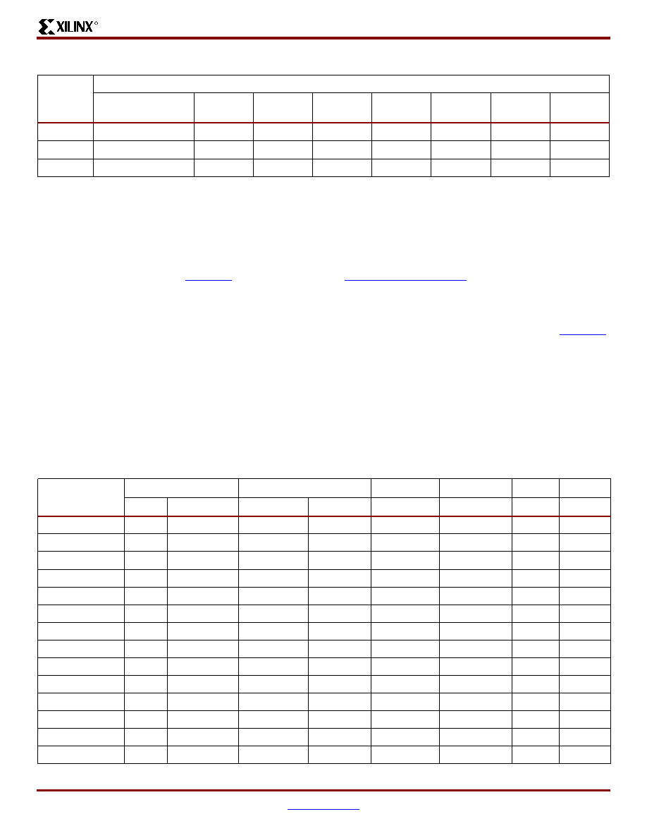
VirtexTM-II Platform FPGAs: DC and Switching Characteristics
R
DS031-3 (v3.1) October 14, 2003
www.xilinx.com
Module 3 of 4
Product Specification
1-800-255-7778
4
General Power Supply Requirements
Proper decoupling of all FPGA power supplies is sessential.
Consult Xilinx Application Note
XAPP623
for detailed infor-
mation on power distribution system design.
V
CCAUX
powers critical resources in the FPGA. Thus,
V
CCAUX
is especially susceptible to power supply noise.
Changes in V
CCAUX
voltage outside of 200 mV peak to peak
should take place at a rate no faster than 10 mV per milli-
second. Techniques to help reduce jitter and period distor-
tion are provided in Xilinx Answer Record 13756, available
at
www.support.xilinx.com
.
V
CCAUX
can share a power plane with 3.3V V
CCO
, but only if
V
CCO
does not have excessive noise. Using simultaneously
switching output (SSO) limits are essential for keeping
power supply noise to a minimum. Refer to
XAPP689
,
"Managing Ground Bounce in Large FPGAs," to determine
the number of simultaneously switching outputs allowed per
bank at the package level.
DC Input and Output Levels
Values for V
IL
and V
IH
are recommended input voltages.
Values for I
OL
and I
OH
are guaranteed over the recom-
mended operating conditions at the V
OL
and V
OH
test
points. Only selected standards are tested. These are cho-
sen to ensure that all standards meet their specifications.
The selected standards are tested at minimum V
CCO
with
the respective V
OL
and V
OH
voltage levels shown. Other
standards are sample tested.
Table 5: Minimum Power On Current Required for Virtex-II Devices
Device (mA)
XC2V40, XC2V80,
XC2V250, XC2V500
XC2V1000
XC2V1500
XC2V2000
XC2V3000
XC2V4000
XC2V6000
XC2V8000
I
CCINTMIN
200
250
350
400
500
650
800
1100
I
CCAUXMIN
100
100
100
100
100
100
100
100
I
CCOMIN
50
50
100
100
100
100
100
100
Notes:
1.
Values specified for power on current parameters are Commercial Grade. For Industrial Grade values, multiply Commercial Grade
values by 1.25.
2.
I
CCOMIN
values listed here apply to the entire device (all banks).
Table 6: DC Input and Output Levels
Input/Output
Standard
V
IL
V
IH
V
OL
V
OH
I
OL
I
OH
V, Min
V, Max
V, Min
V, Max
V, Max
V, Min
mA
mA
LVTTL
(1)
≠ 0.5
0.8
2.0
3.6
0.4
2.4
24
≠ 24
LVCMOS33
≠ 0.5
0.8
2.0
3.6
0.4
V
CCO
≠ 0.4
24
≠ 24
LVCMOS25
≠ 0.5
0.7
1.7
2.7
0.4
V
CCO
≠ 0.4
24
≠ 24
LVCMOS18
≠ 0.5
35% V
CCO
65% V
CCO
1.95
0.4
V
CCO
≠ 0.4
16
≠ 16
LVCMOS15
≠ 0.5
35% V
CCO
65% V
CCO
1.7
0.4
V
CCO
≠ 0.4
16
≠ 16
PCI33_3
≠ 0.5
30% V
CCO
50% V
CCO
V
CCO
+ 0.5
10% V
CCO
90% V
CCO
Note 2
Note 2
PCI66_3
≠ 0.5
30% V
CCO
50% V
CCO
V
CCO
+ 0.5
10% V
CCO
90% V
CCO
Note 2
Note 2
PCI≠X
≠ 0.5
Note 2
Note 2
Note 2
Note 2
Note 2
Note 2
Note 2
GTLP
≠ 0.5
V
REF
≠ 0.1
V
REF
+ 0.1
V
CCO
+ 0.5
0.6
n/a
36
n/a
GTL
≠ 0.5
V
REF
≠ 0.05
V
REF
+ 0.05
V
CCO
+ 0.5
0.4
n/a
40
n/a
HSTL I
≠ 0.5
V
REF
≠ 0.1
V
REF
+ 0.1
V
CCO
+ 0.5
0.4
V
CCO
≠ 0.4
8
≠ 8
HSTL II
≠ 0.5
V
REF
≠ 0.1
V
REF
+ 0.1
V
CCO
+ 0.5
0.4
V
CCO
≠ 0.4
16
≠ 16
HSTL III
≠ 0.5
V
REF
≠ 0.1
V
REF
+ 0.1
V
CCO
+ 0.5
0.4
V
CCO
≠ 0.4
24
≠ 8
HSTL IV
≠ 0.5
V
REF
≠ 0.1
V
REF
+ 0.1
V
CCO
+ 0.5
0.4
V
CCO
≠ 0.4
48
≠ 8
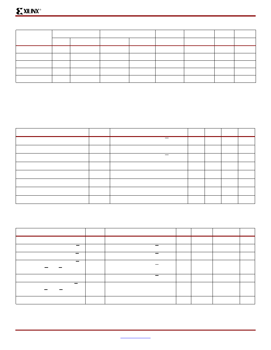
VirtexTM-II Platform FPGAs: DC and Switching Characteristics
R
DS031-3 (v3.1) October 14, 2003
www.xilinx.com
Module 3 of 4
Product Specification
1-800-255-7778
5
LDT Differential Signal DC Specifications (LDT_25)
LVDS DC Specifications (LVDS_33 & LVDS_25)
SSTL3 I
≠ 0.5
V
REF
≠ 0.2
V
REF
+ 0.2
V
CCO
+ 0.5
V
REF
≠ 0.6
V
REF
+ 0.6
8
≠ 8
SSTL3 II
≠ 0.5
V
REF
≠ 0.2
V
REF
+ 0.2
V
CCO
+ 0.5
V
REF
≠ 0.8
V
REF
+ 0.8
16
≠ 16
SSTL2 I
≠ 0.5
V
REF
≠ 0.15
V
REF
+ 0.15
V
CCO
+ 0.5
V
REF
≠ 0.65
V
REF
+ 0.65
7.6
≠ 7.6
SSTL2 II
≠ 0.5
V
REF
≠ 0.15
V
REF
+ 0.15
V
CCO
+ 0.5
V
REF
≠ 0.80
V
REF
+ 0.80
15.2
≠ 15.2
AGP
≠ 0.5
V
REF
≠ 0.2
V
REF
+ 0.2
V
CCO
+ 0.5
10% V
CCO
90% V
CCO
Note 2
Note 2
Notes:
1.
V
OL
and V
OH
for lower drive currents are sample tested. The DONE pin is always LVTTL 12 mA.
2.
Tested according to the relevant specifications.
3.
LVTTL and LVCMOS inputs have approximately 100 mV of hysteresis.
Table 6: DC Input and Output Levels (Continued)
Input/Output
Standard
V
IL
V
IH
V
OL
V
OH
I
OL
I
OH
V, Min
V, Max
V, Min
V, Max
V, Max
V, Min
mA
mA
Table 7: LDT DC Specifications
DC Parameter
Symbol
Conditions
Min
Typ
Max
Units
Differential Output Voltage
V
OD
R
T
= 100
across Q and Q signals
500
600
700
mV
Change in V
OD
Magnitude
V
OD
≠
15
15
mV
Output Common Mode Voltage
V
OCM
R
T
= 100
across Q and Q signals
560
600
640
mV
Change in V
OS
Magnitude
V
OCM
≠
15
15
mV
Input Differential Voltage
V
ID
200
600
1000
mV
Change in V
ID
Magnitude
V
ID
≠
15
15
mV
Input Common Mode Voltage
V
ICM
500
600
700
mV
Change in V
ICM
Magnitude
V
ICM
≠
15
15
mV
Table 8: LVDS DC Specifications
DC Parameter
Symbol
Conditions
Min
Typ
Max
Units
Supply Voltage
V
CCO
3.3 or 2.5
V
Output High Voltage for Q and Q
V
OH
R
T
= 100
across Q and Q signals
1.575
V
Output Low Voltage for Q and Q
V
OL
R
T
= 100
across Q and Q signals
0.925
V
Differential Output Voltage (Q ≠ Q),
Q = High (Q ≠ Q), Q = High
V
ODIFF
R
T
= 100
across Q and Q signals
250
350
400
mV
Output Common-Mode Voltage
V
OCM
R
T
= 100
across Q and Q signals
1.125
1.2
1.375
V
Differential Input Voltage (Q ≠ Q),
Q = High (Q ≠ Q), Q = High
V
IDIFF
Common-mode input voltage = 1.25 V
100
350
N/A
mV
Input Common-Mode Voltage
V
ICM
Differential input voltage =
±350 mV
0.2
1.25
V
CCO
≠ 0.5
V
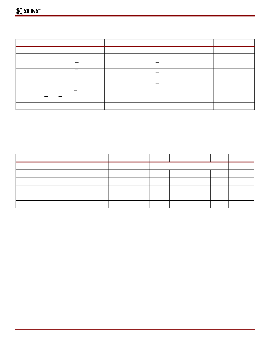
VirtexTM-II Platform FPGAs: DC and Switching Characteristics
R
DS031-3 (v3.1) October 14, 2003
www.xilinx.com
Module 3 of 4
Product Specification
1-800-255-7778
6
Extended LVDS DC Specifications
(LVDSEXT_33 & LVDSEXT_25)
LVPECL DC Specifications
These values are valid when driving a 100
differential
load only, i.e., a 100
resistor between the two receiver
pins. The V
OH
levels are 200 mV below standard LVPECL
levels and are compatible with devices tolerant of lower
common-mode ranges.
Table 10
summarizes the DC output
specifications of LVPECL. For more information on using
LVPECL
,
see the Virtex-II User Guide.
Table 9: Extended LVDS DC Specifications
DC Parameter
Symbol
Conditions
Min
Typ
Max
Units
Supply Voltage
V
CCO
3.3 or 2.5
V
Output High voltage for Q and Q
V
OH
R
T
= 100
across Q and Q signals
1.785
V
Output Low voltage for Q and Q
V
OL
R
T
= 100
across Q and Q signals
0.705
V
Differential output voltage (Q ≠ Q),
Q = High (Q ≠ Q), Q = High
V
ODIFF
R
T
= 100
across Q and Q signals
440
820
mV
Output common-mode voltage
V
OCM
R
T
= 100
across Q and Q signals
1.125
1.200
1.375
V
Differential input voltage (Q ≠ Q),
Q = High (Q ≠ Q), Q = High
V
IDIFF
Common-mode input voltage = 1.25 V
100
350
N/A
mV
Input common-mode voltage
V
ICM
Differential input voltage =
±350 mV
0.2
1.25
V
CCO
≠ 0.5
V
Table 10: LVPECL DC Specifications
DC Parameter
Min
Max
Min
Max
Min
Max
Units
V
CCO
3.0
3.3
3.6
V
V
OH
1.8
2.11
1.92
2.28
2.13
2.41
V
V
OL
0.96
1.27
1.06
1.43
1.30
1.57
V
V
IH
1.49
2.72
1.49
2.72
1.49
2.72
V
V
IL
0.86
2.125
0.86
2.125
0.86
2.125
V
Differential Input Voltage
0.3
≠
0.3
≠
0.3
≠
V
VirtexTM-II Platform FPGAs: DC and Switching Characteristics
R
DS031-3 (v3.1) October 14, 2003
www.xilinx.com
Module 3 of 4
Product Specification
1-800-255-7778
7
Virtex-II
Performance Characteristics
This section provides the performance characteristics of
some common functions and designs implemented in
Virtex-II devices. The numbers reported here are worst-case
values; they have all been fully characterized. Note that
these values are subject to the same guidelines as
Virtex-II
Switching Characteristics, page 9
(speed files).
Table 11
provides pin-to-pin values (in nanoseconds)
including IOB delays; that is, delay through the device from
input pin to output pin. In the case of multiple inputs and out-
puts, the worst delay is reported.
Table 12
shows internal (register-to-register) performance. Values are reported in MHz.
Table 11: Pin-to-Pin Performance
Description
Device Used & Speed Grade
Pin-to-Pin (with I/O delays)
Units
Basic Functions
16-bit Address Decoder
XC2V1000 -5
6.3
ns
32-bit Address Decoder
XC2V1000 -5
7.7
ns
64-bit Address Decoder
XC2V1000 -5
9.3
ns
4:1 MUX
XC2V1000 -5
5.7
ns
8:1 MUX
XC2V1000 -5
6.5
ns
16:1 MUX
XC2V1000 -5
6.7
ns
32:1 MUX
XC2V1000 -5
8.7
ns
Combinatorial (pad to LUT to pad)
XC2V1000 -5
5.0
ns
Memory
Block RAM
Pad to setup
1.6
ns
Clock to Pad
9.5
ns
Distributed RAM
Pad to setup
XC2V1000 -5
2.7
ns
Clock to Pad
XC2V1000 -5
5.1 (no clk skew)
ns
Table 12: Register-to-Register Performance
Description
Device Used & Speed
Grade
Register-to-Register
Performance
Units
Basic Functions
16-bit Address Decoder
XC2V1000 -5
398
MHz
32-bit Address Decoder
XC2V1000 -5
291
MHz
64-bit Address Decoder
XC2V1000 -5
274
MHz
4:1 MUX
XC2V1000 -5
563
MHz
8:1 MUX
XC2V1000 -5
454
MHz
16:1 MUX
XC2V1000 -5
414
MHz
32:1 MUX
XC2V1000 -5
323
MHz
Register to LUT to Register
XC2V1000 -5
613
MHz

VirtexTM-II Platform FPGAs: DC and Switching Characteristics
R
DS031-3 (v3.1) October 14, 2003
www.xilinx.com
Module 3 of 4
Product Specification
1-800-255-7778
8
8-bit Adder
XC2V1000 -5
292
MHz
16-bit Adder
XC2V1000 -5
239
MHz
64-bit Adder
XC2V1000 -5
114
MHz
64-bit Counter
XC2V1000 -5
114
MHz
64-bit Accumulator
XC2V1000 -5
110
MHz
Multiplier 18x18 (with Block RAM inputs)
XC2V1000 -5
88
MHz
Multiplier 18x18 (with Register inputs)
XC2V1000 -5
105
MHz
Memory
Block RAM
Single-Port 4096 x 4 bits
278
MHz
Single-Port 2048 x 9 bits
277
MHz
Single-Port 1024 x 18 bits
270
MHz
Single-Port 512 x 36 bits
253
MHz
Dual-Port A:4096 x 4 bits & B:1024 x 18 bits
257
MHz
Dual-Port A:1024 x 18 bits & B:1024 x 18 bits
259
MHz
Dual-Port A:2048 x 9 bits & B: 512 x 36 bits
250
MHz
Distributed RAM
Single-Port 32 x 8-bit
XC2V1000 -5
387
MHz
Single-Port 64 x 8-bit
XC2V1000 -5
335
MHz
Single-Port 128 x 8-bit
XC2V1000 -5
266
MHz
Dual-Port 16 x 8
XC2V1000 -5
409
MHz
Dual-Port 32 x 8
XC2V1000 -5
311
MHz
Dual-Port 64 x 8
XC2V1000 -5
294
MHz
Shift Registers
128-bit SRL
N/A
MHz
256-bit SRL
N/A
MHz
FIFOs (Async. in Block RAM)
1024 x 18-bit Read
279
MHz
1024 x 18-bit Write
172
MHz
FIFOs (Sync. in SRL)
128 x 8-bit
N/A
MHz
128 x 16-bit
N/A
MHz
Table 12: Register-to-Register Performance (Continued)
Description
Device Used & Speed
Grade
Register-to-Register
Performance
Units
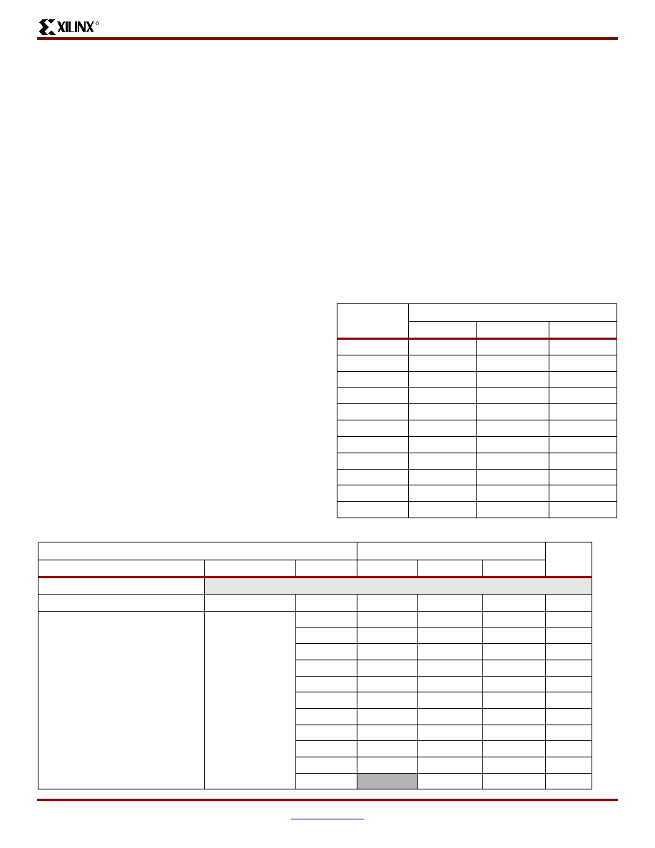
VirtexTM-II Platform FPGAs: DC and Switching Characteristics
R
DS031-3 (v3.1) October 14, 2003
www.xilinx.com
Module 3 of 4
Product Specification
1-800-255-7778
9
Virtex-II Switching Characteristics
Switching characteristics in this document are specified on
a per-speed-grade basis and can be designated as
Advance, Preliminary, or Production. Note that
Virtex-II
Performance Characteristics, page 7
are subject to these
guidelines as well. Each designation is defined as follows:
Advance: These speed files are based on simulations only
and are typically available soon after device design specifi-
cations are frozen. Although speed grades with this desig-
nation are considered relatively stable and conservative,
some under-reporting might still occur.
Preliminary: These speed files are based on complete ES
(engineering sample) silicon characterization. Devices and
speed grades with this designation are intended to give a
better indication of the expected performance of production
silicon. The probability of under-reporting delays is greatly
reduced as compared to Advance data.
Production: These speed files are released once enough
production silicon of a particular device family member has
been characterized to provide full correlation between
speed files and devices over numerous production lots.
There is no under-reporting of delays, and customers
receive formal notification of any subsequent changes. Typ-
ically, the slowest speed grades transition to Production
before faster speed grades.
Since individual family members are produced at different
times, the migration from one category to another depends
completely on the status of the fabrication process for each
device.
Table 13
correlates the current status of each
Virtex-II device with a corresponding speed grade designa-
tion.
All specifications are always representative of worst-case
supply voltage and junction temperature conditions.
Testing of Switching Characteristics
All devices are 100% functionally tested. Internal timing
parameters are derived from measuring internal test pat-
terns. Listed below are representative values. For more
specific, more precise, and worst-case guaranteed data,
use the values reported by the Xilinx static timing analyzer
and back-annotate to the simulation net list. Unless other-
wise noted, values apply to all Virtex-II devices.
IOB
Input Switching Characteristics
Input delays associated with the pad are specified for
LVTTL levels. For other standards, adjust the delays with
the values shown in
IOB Input Switching Characteristics
Standard Adjustments, page 11
.
Table 13: Virtex-II Device Speed Grade Designations
Device
Speed Grade Designations
Advance
Preliminary
Production
XC2V40
-6, -5, -4
XC2V80
-6, -5, -4
XC2V250
-6, -5, -4
XC2V500
-6, -5, -4
XC2V1000
-6, -5, -4
XC2V1500
-6, -5, -4
XC2V2000
-6, -5, -4
XC2V3000
-6, -5, -4
XC2V4000
-6, -5, -4
XC2V6000
-6, -5, -4
XC2V8000
-5, -4
Table 14: IOB Input Switching Characteristics
Speed Grade
Units
Description
Symbol
Device
-6
-5
-4
Propagation Delays
Pad to I output, no delay
T
IOPI
All
0.69
0.76
0.88
ns, Max
Pad to I output, with delay
T
IOPID
XC2V40
1.92
2.11
2.43
ns, Max
XC2V80
1.92
2.11
2.43
ns, Max
XC2V250
1.92
2.11
2.43
ns, Max
XC2V500
1.92
2.11
2.43
ns, Max
XC2V1000
1.92
2.11
2.43
ns, Max
XC2V1500
1.92
2.11
2.43
ns, Max
XC2V2000
1.92
2.11
2.43
ns, Max
XC2V3000
1.97
2.16
2.49
ns, Max
XC2V4000
1.97
2.16
2.49
ns, Max
XC2V6000
2.10
2.31
2.66
ns, Max
XC2V8000
2.31
2.66
ns, Max
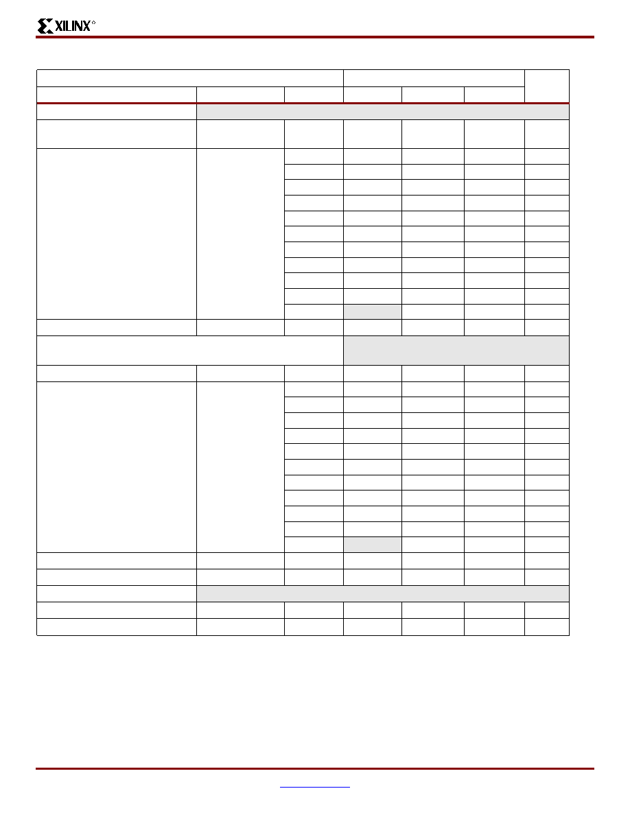
VirtexTM-II Platform FPGAs: DC and Switching Characteristics
R
DS031-3 (v3.1) October 14, 2003
www.xilinx.com
Module 3 of 4
Product Specification
1-800-255-7778
10
Propagation Delays
Pad to output IQ via transparent
latch, no delay
T
IOPLI
All
0.83
0.91
1.05
ns, Max
Pad to output IQ via transparent
latch, with delay
T
IOPLID
XC2V40
3.23
3.55
4.09
ns, Max
XC2V80
3.23
3.55
4.09
ns, Max
XC2V250
3.23
3.55
4.09
ns, Max
XC2V500
3.23
3.55
4.09
ns, Max
XC2V1000
3.23
3.55
4.09
ns, Max
XC2V1500
3.23
3.55
4.09
ns, Max
XC2V2000
3.23
3.55
4.09
ns, Max
XC2V3000
3.32
3.65
4.20
ns, Max
XC2V4000
3.32
3.65
4.20
ns, Max
XC2V6000
3.60
3.95
4.55
ns, Max
XC2V8000
3.95
4.55
ns, Max
Clock CLK to output IQ
T
IOCKIQ
All
0.67
0.77
ns, Max
Setup and Hold Times With Respect to Clock at IOB Input
Register
Pad, no delay
T
IOPICK
/T
IOICKP
All
0.84/≠0.36
0.92/≠0.39
1.06/≠0.45
ns, Min
Pad, with delay
T
IOPICKD
/T
IOICKPD
XC2V40
3.24/≠2.04
3.57/≠2.24
4.10/≠2.58
ns, Min
XC2V80
3.24/≠2.04
3.57/≠2.24
4.10/≠2.58
ns, Min
XC2V250
3.24/≠2.04
3.57/≠2.24
4.10/≠2.58
ns, Min
XC2V500
3.24/≠2.04
3.57/≠2.24
4.10/≠2.58
ns, Min
XC2V1000
3.24/≠2.04
3.57/≠2.24
4.10/≠2.58
ns, Min
XC2V1500
3.24/≠2.04
3.57/≠2.24
4.10/≠2.58
ns, Min
XC2V2000
3.24/≠2.04
3.57/≠2.24
4.10/≠2.58
ns, Min
XC2V3000
3.33/≠2.10
3.67/≠2.31
4.22/≠2.66
ns, Min
XC2V4000
3.33/≠2.10
3.67/≠2.31
4.22/≠2.66
ns, Min
XC2V6000
3.61/≠2.29
3.97/≠2.52
4.56/≠2.90
ns, Min
XC2V8000
3.97/≠2.52
4.56/≠2.90
ns, Min
ICE input
T
IOICECK
/T
IOCKICE
All
0.21/ 0.04
0.24/ 0.04
ns, Min
SR input (IFF, synchronous)
T
IOSRCKI
All
0.27
0.30
0.34
ns, Min
Set/Reset Delays
SR input to IQ (asynchronous)
T
IOSRIQ
All
1.11
1.22
1.40
ns, Max
GSR to output IQ
T
GSRQ
All
5.44
5.98
6.88
ns, Max
Notes:
1.
Input timing for LVTTL is measured at 1.4 V. For other I/O standards, see
Table 18
.
Table 14: IOB Input Switching Characteristics (Continued)
Speed Grade
Units
Description
Symbol
Device
-6
-5
-4
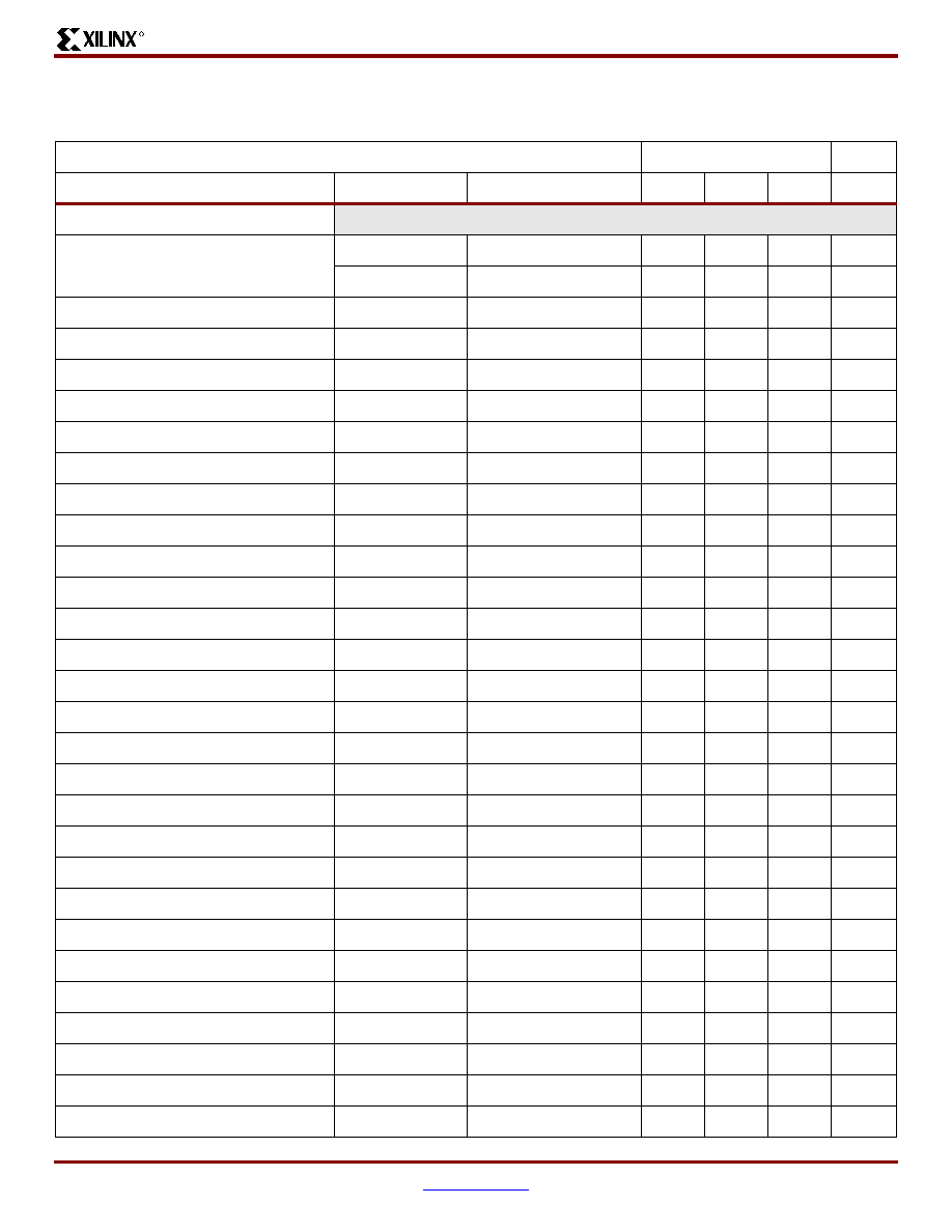
VirtexTM-II Platform FPGAs: DC and Switching Characteristics
R
DS031-3 (v3.1) October 14, 2003
www.xilinx.com
Module 3 of 4
Product Specification
1-800-255-7778
11
IOB Input Switching Characteristics Standard Adjustments
Table 15: IOB Input Switching Characteristics Standard Adjustments
Speed Grade
Description
Symbol
Standard
-6
-5
-4
Units
Data Input Delay Adjustments
Standard-specific data input delay
adjustments
T
ILVTTL
LVTTL
0.00
0.00
0.00
ns
T
ILVCMOS33
LVCMOS33
0.00
0.00
0.00
ns
T
ILVCMOS25
LVCMOS25
0.11
0.11
0.12
ns
T
ILVCMOS18
LVCMOS18
0.42
0.43
0.49
ns
T
ILVCMOS15
LVCMOS15
0.98
1.00
1.15
ns
T
ILVDS_25
LVDS_25
0.60
0.60
0.69
ns
T
ILVDS_33
LVDS_33
0.60
0.60
0.69
ns
T
ILVPECL_33
LVPECL
0.60
0.60
0.69
ns
T
IPCI33_3
PCI, 33 MHz, 3.3 V
0.00
0.00
0.00
ns
T
IPCI66_3
PCI, 66 MHz, 3.3 V
0.00
0.00
0.00
ns
T
IPCIX
PCI
≠
X, 133 MHz, 3.3 V
0.00
0.00
0.00
ns
T
IGTL
GTL
0.42
0.42
0.48
ns
T
IGTLP
GTLP
0.42
0.42
0.48
ns
T
IHSTL_I
HSTL I
0.42
0.42
0.48
ns
T
IHSTL_II
HSTL II
0.42
0.42
0.48
ns
T
IHSTL_III
HSTL III
0.42
0.42
0.48
ns
T
IHSTL_IV
HSTL IV
0.42
0.42
0.48
ns
T
IHSTL_I_18
HSTL I_18
0.42
0.42
0.48
ns
T
IHSTL_II_18
HSTL II_18
0.42
0.42
0.48
ns
T
IHSTL_III_18
HSTL III_18
0.42
0.42
0.48
ns
T
IHSTL_IV_18
HSTL IV_18
0.42
0.42
0.48
ns
T
ISSTL2_I
SSTL2 I
0.42
0.42
0.48
ns
T
ISSTL2_II
SSTL2 II
0.42
0.42
0.48
ns
T
ISSTL3_I
SSTL3 I
0.35
0.35
0.40
ns
T
ISSTL3_II
SSTL3 II
0.35
0.35
0.40
ns
T
IAGP
AGP
0.35
0.35
0.40
ns
T
ILVDCI_33
LVDCI_33
0.00
0.00
0.00
ns
T
ILVDCI_25
LVDCI_25
0.11
0.11
0.12
ns
T
ILVDCI_18
LVDCI_18
0.42
0.43
0.49
ns

VirtexTM-II Platform FPGAs: DC and Switching Characteristics
R
DS031-3 (v3.1) October 14, 2003
www.xilinx.com
Module 3 of 4
Product Specification
1-800-255-7778
12
T
ILVDCI_15
LVDCI_15
0.98
1.00
1.14
ns
T
ILVDCI_DV2_33
LVDCI_DV2_33
0.00
0.00
0.00
ns
T
ILVDCI_DV2_25
LVDCI_DV2_25
0.11
0.11
0.12
ns
T
ILVDCI_DV2_18
LVDCI_DV2_18
0.42
0.43
0.49
ns
T
ILVDCI_DV2_15
LVDCI_DV2_15
0.98
1.00
1.14
ns
T
IGTL_DCI
GTL_DCI
0.42
0.42
0.48
ns
T
IGTLP_DCI
GTLP_DCI
0.42
0.42
0.48
ns
T
IHSTL_I_DCI
HSTL_I_DCI
0.42
0.42
0.48
ns
T
IHSTL_II_DCI
HSTL_II_DCI
0.42
0.42
0.48
ns
T
IHSTL_III_DCI
HSTL_III_DCI
0.42
0.42
0.48
ns
T
IHSTL_IV_DCI
HSTL_IV_DCI
0.42
0.42
0.48
ns
T
IHSTL_I_DCI_18
HSTL_I_DCI_18
0.42
0.42
0.48
ns
T
IHSTL_II_DCI_18
HSTL_II_DCI_18
0.42
0.42
0.48
ns
T
IHSTL_III_DCI_18
HSTL_III_DCI_18
0.42
0.42
0.48
ns
T
IHSTL_IV_DCI_18
HSTL_IV_DCI_18
0.42
0.42
0.48
ns
T
ISSTL2_I_DCI
SSTL2_I_DCI
0.42
0.42
0.48
ns
T
ISSTL2_II_DCI
SSTL2_II_DCI
0.42
0.42
0.48
ns
T
ISSTL3_I_DCI
SSTL3_I_DCI
0.35
0.35
0.40
ns
T
ISSTL3_II_DCI
SSTL3_II_DCI
0.35
0.35
0.40
ns
T
ILDT_25
LDT_25
0.48
0.49
0.56
ns
T
IULVDS_25
ULVDS_25
0.48
0.49
0.56
ns
Notes:
1.
Input timing for LVTTL is measured at 1.4 V. For other I/O standards, see
Table 18
.
Table 15: IOB Input Switching Characteristics Standard Adjustments (Continued)
Speed Grade
Description
Symbol
Standard
-6
-5
-4
Units
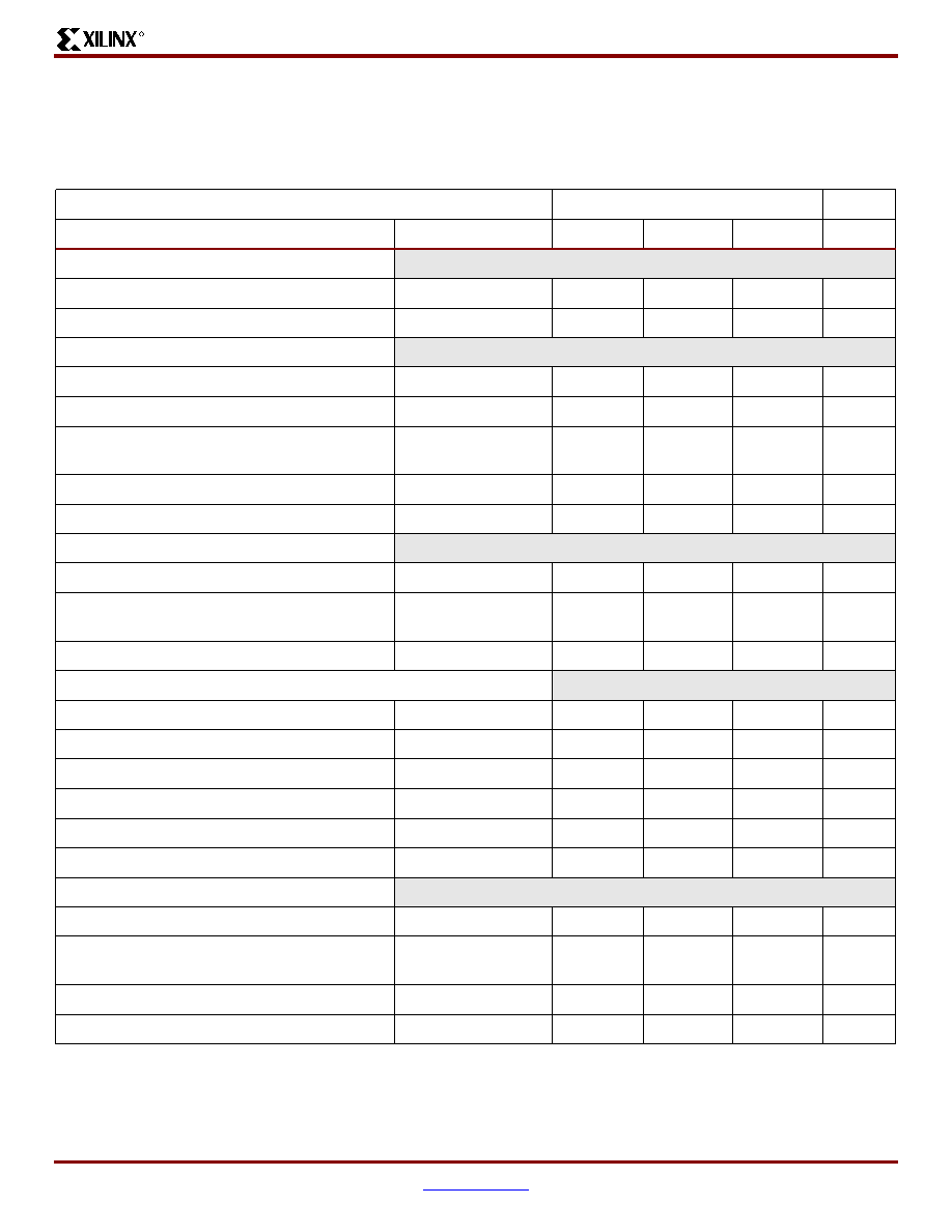
VirtexTM-II Platform FPGAs: DC and Switching Characteristics
R
DS031-3 (v3.1) October 14, 2003
www.xilinx.com
Module 3 of 4
Product Specification
1-800-255-7778
13
IOB Output Switching Characteristics
Output delays terminating at a pad are specified for LVTTL with 12 mA drive and fast slew rate. For other standards, adjust
the delays with the values shown in
IOB Output Switching Characteristics Standard Adjustments, page 14
.
Table 16: IOB Output Switching Characteristics
Speed Grade
Description
Symbol
-6
-5
-4
Units
Propagation Delays
O input to Pad
T
IOOP
1.43
1.51
1.74
ns, Max
O input to Pad via transparent latch
T
IOOLP
1.72
1.83
2.11
ns, Max
3-State Delays
T input to Pad high-impedance
(1)
T
IOTHZ
0.51
0.56
0.64
ns, Max
T input to valid data on Pad
T
IOTP
1.38
1.45
1.67
ns, Max
T input to Pad high-impedance via transparent
latch
(1)
T
IOTLPHZ
0.80
0.88
1.01
ns, Max
T input to valid data on Pad via transparent latch
T
IOTLPON
1.67
1.77
2.04
ns, Max
GTS to Pad high impedance
(1)
T
GTS
4.73
5.20
5.98
ns, Max
Sequential Delays
Clock CLK to Pad
T
IOCKP
1.76
1.87
2.15
ns, Max
Clock CLK to Pad high-impedance
(synchronous)
(1)
T
IOCKHZ
0.95
1.04
1.20
ns, Max
Clock CLK to valid data on Pad (synchronous)
T
IOCKON
1.82
1.94
2.22
ns, Max
Setup and Hold Times Before/After Clock CLK
O input
T
IOOCK
/T
IOCKO
0.31/≠0.08
0.34/≠0.09
0.39/≠0.11
ns, Min
OCE input
T
IOOCECK
/T
IOCKOCE
0.19/≠0.06
0.21/≠0.07
0.24/≠0.08
ns, Min
SR input (OFF)
T
IOSRCKO
/T
IOCKOSR
0.27/≠0.05
0.30/≠0.06
0.34/≠0.07
ns, Min
3
≠
State Setup Times, T input
T
IOTCK
/T
IOCKT
0.28/≠0.06
0.31/≠0.07
0.35/≠0.08
ns, Min
3
≠
State Setup Times, TCE input
T
IOTCECK
/T
IOCKTCE
0.19/≠0.06
0.21/≠0.07
0.24/≠0.08
ns, Min
3
≠
State Setup Times, SR input (TFF)
T
IOSRCKT
/T
IOCKTSR
0.27/≠0.05
0.30/≠0.06
0.34/≠0.07
ns, Min
Set/Reset Delays
SR input to Pad (asynchronous)
T
IOSRP
2.41
2.59
2.98
ns, Max
SR input to Pad high-impedance
(asynchronous)
(1)
T
IOSRHZ
1.52
1.67
1.92
ns, Max
SR input to valid data on Pad (asynchronous)
T
IOSRON
2.39
2.56
2.95
ns, Max
GSR to Pad
T
IOGSRQ
5.44
5.98
6.88
ns, Max
Notes:
1.
The 3-state turn-off delays should not be adjusted.

VirtexTM-II Platform FPGAs: DC and Switching Characteristics
R
DS031-3 (v3.1) October 14, 2003
www.xilinx.com
Module 3 of 4
Product Specification
1-800-255-7778
14
IOB Output Switching Characteristics Standard Adjustments
Output delays terminating at a pad are specified for LVTTL with 12 mA drive and fast slew rate. For other standards, adjust
the delays by the values shown.
Table 17: IOB Output Switching Characteristics Standard Adjustments
Speed Grade
Description
Symbol
Standard
-6
-5
-4
Units
Output Delay Adjustments
Standard-specific adjustments for output
delays terminating at pads (based on
standard capacitive load, Csl)
T
OLVTTL_S2
LVTTL, Slow, 2 mA
9.42
9.71
10.68
ns
T
OLVTTL_S4
4 mA
5.77
5.95
6.55
ns
T
OLVTTL_S6
6 mA
4.11
4.24
4.66
ns
T
OLVTTL_S8
8 mA
2.87
2.96
3.26
ns
T
OLVTTL_S12
12 mA
2.32
2.39
2.63
ns
T
OLVTTL_S16
16 mA
1.70
1.75
1.93
ns
T
OLVTTL_S24
24 mA
1.26
1.30
1.43
ns
T
OLVTTL_F2
LVTTL, Fast, 2 mA
6.52
6.72
7.39
ns
T
OLVTTL_F4
4 mA
2.80
2.88
3.17
ns
T
OLVTTL_F6
6 mA
1.57
1.62
1.78
ns
T
OLVTTL_F8
8 mA
0.46
0.48
0.52
ns
T
OLVTTL_F12
12 mA
0.00
0.00
0.00
ns
T
OLVTTL_F16
16 mA
≠0.13
≠0.14
≠0.15
ns
T
OLVTTL_F24
24 mA
≠0.22
≠0.23
≠0.26
ns
T
OLVDS_25
LVDS ≠0.31
≠0.32
≠0.36
ns
T
OLVDS_33
LVDS ≠0.25
≠0.26
≠0.29
ns
T
OLVDSEXT_25
LVDS ≠0.18
≠0.19
≠0.21
ns
T
OLVDSEXT_33
LVDS ≠0.17
≠0.18
≠0.19
ns
T
OLDT_25
LDT ≠0.20
≠0.21
≠0.23
ns
T
OBLVDS_25
BLVDS
0.67
0.69
0.76
ns
T
OULVDS_25
ULVDS
≠0.20
≠0.21
≠0.23
ns
T
OLVPECL_33
LVPECL
0.29
0.30
0.33
ns
T
OPCI33_3
PCI, 33 MHz, 3.3 V
1.15
1.19
1.31
ns
T
OPCI66_3
PCI, 66 MHz, 3.3 V
≠0.01
≠0.01
≠0.01
ns
T
OPCIX
PCI≠X, 133 MHz, 3.3 V
≠0.01
≠0.01
≠0.01
ns
T
OGTL
GTL
≠0.31
≠0.32
≠0.36
ns
T
OGTLP
GTLP
≠0.17
≠0.18
≠0.20
ns
T
OHSTL_I
HSTL I
0.26
0.27
0.29
ns
T
OHSTL_II
HSTL II
≠0.15
≠0.16
≠0.17
ns
T
OHSTL_III
HSTL III
≠0.17
≠0.17
≠0.19
ns
T
OHSTL_IV
HSTL IV
≠0.40
≠0.41
≠0.45
ns
T
OHSTL_I_18
HSTL I_18
0.03
0.03
0.04
ns
T
OHSTL_II_18
HSTL II_18
≠0.17
≠0.18
≠0.20
ns
T
OHSTL_III_18
HSTL III_18
≠0.16
≠0.16
≠0.18
ns
T
OHSTL_IV_18
HSTL IV_18
≠0.39
≠0.40
≠0.44
ns

VirtexTM-II Platform FPGAs: DC and Switching Characteristics
R
DS031-3 (v3.1) October 14, 2003
www.xilinx.com
Module 3 of 4
Product Specification
1-800-255-7778
15
T
OSSTL2_I
SSTL2 I
0.21
0.22
0.24
ns
T
OSSTL2_II
SSTL2 II
≠0.15
≠0.16
≠0.18
ns
T
OSSTL3_I
SSTL3 I
0.29
0.30
0.33
ns
T
OSSTL3_II
SSTL3 II
≠0.05
≠0.05
≠0.05
ns
T
OAGP
AGP
≠0.27
≠0.28
≠0.31
ns
T
OLVCMOS33_S2
LVCMOS33, Slow, 2 mA
7.67
7.91
8.70
ns
T
OLVCMOS33_S4
4 mA
4.37
4.50
4.95
ns
T
OLVCMOS33_S6
6 mA
3.34
3.44
3.78
ns
T
OLVCMOS33_S8
8 mA
2.29
2.36
2.60
ns
T
OLVCMOS33_S12
12 mA
1.91
1.97
2.16
ns
T
OLVCMOS33_S16
16 mA
1.24
1.27
1.40
ns
T
OLVCMOS33_S24
24 mA
1.18
1.22
1.34
ns
T
OLVCMOS33_F2
LVCMOS33, Fast, 2 mA
5.82
6.00
6.60
ns
T
OLVCMOS33_F4
4 mA
2.48
2.55
2.81
ns
T
OLVCMOS33_F6
6 mA
1.28
1.31
1.45
ns
T
OLVCMOS33_F8
8 mA
0.48
0.49
0.54
ns
T
OLVCMOS33_F12
12 mA
0.27
0.28
0.31
ns
T
OLVCMOS33_F16
16 mA
≠0.14
≠0.14
≠0.15
ns
T
OLVCMOS33_F24
24 mA
≠0.21
≠0.21
≠0.23
ns
T
OLVCMOS25_S2
LVCMOS25, Slow, 2 mA
9.11
9.39
10.33
ns
T
OLVCMOS25_S4
4 mA
5.00
5.16
5.67
ns
T
OLVCMOS25_S6
6 mA
4.53
4.67
5.13
ns
T
OLVCMOS25_S8
8 mA
3.86
3.98
4.38
ns
T
OLVCMOS25_S12
12 mA
2.84
2.93
3.22
ns
T
OLVCMOS25_S16
16 mA
2.36
2.43
2.67
ns
T
OLVCMOS25_S24
24 mA
2.00
2.06
2.27
ns
T
OLVCMOS25_F2
LVCMOS25, Fast, 2 mA
4.06
4.18
4.60
ns
T
OLVCMOS25_F4
4 mA
1.15
1.18
1.30
ns
T
OLVCMOS25_F6
6 mA
0.72
0.74
0.81
ns
T
OLVCMOS25_F8
8 mA
0.33
0.34
0.37
ns
T
OLVCMOS25_F12
12 mA
0.02
0.02
0.03
ns
T
OLVCMOS25_F16
16 mA
≠0.18
≠0.19
≠0.21
ns
T
OLVCMOS25_F24
24 mA
≠0.35
≠0.36
≠0.40
ns
T
OLVCMOS18_S2
LVCMOS18, Slow, 2 mA
15.62
16.10
17.71
ns
T
OLVCMOS18_S4
4 mA
10.20
10.51
11.57
ns
T
OLVCMOS18_S6
6 mA
7.52
7.75
8.53
ns
T
OLVCMOS18_S8
8 mA
6.87
7.08
7.78
ns
T
OLVCMOS18_S12
12 mA
5.54
5.71
6.28
ns
T
OLVCMOS18_S16
16 mA
5.31
5.47
6.02
ns
T
OLVCMOS18_F2
LVCMOS18, Fast, 2 mA
5.55
5.72
6.30
ns
Table 17: IOB Output Switching Characteristics Standard Adjustments (Continued)
Speed Grade
Description
Symbol
Standard
-6
-5
-4
Units

VirtexTM-II Platform FPGAs: DC and Switching Characteristics
R
DS031-3 (v3.1) October 14, 2003
www.xilinx.com
Module 3 of 4
Product Specification
1-800-255-7778
16
T
OLVCMOS18_F4
4 mA
1.89
1.95
2.15
ns
T
OLVCMOS18_F6
6 mA
0.83
0.85
0.94
ns
T
OLVCMOS18_F8
8 mA
0.70
0.72
0.80
ns
T
OLVCMOS18_F12
12 mA
0.26
0.27
0.30
ns
T
OLVCMOS18_F16
16 mA
0.23
0.23
0.26
ns
T
OLVCMOS15_S2
LVCMOS15, Slow, 2 mA
18.96
19.55
21.50
ns
T
OLVCMOS15_S4
4 mA
12.77
13.17
14.48
ns
T
OLVCMOS15_S6
6 mA
12.05
12.42
13.66
ns
T
OLVCMOS15_S8
8 mA
9.75
10.06
11.06
ns
T
OLVCMOS15_S12
12 mA
9.04
9.32
10.25
ns
T
OLVCMOS15_S16
16 mA
8.21
8.46
9.31
ns
T
OLVCMOS15_F2
LVCMOS15, Fast, 2 mA
5.09
5.25
5.78
ns
T
OLVCMOS15_F4
4 mA
2.01
2.07
2.27
ns
T
OLVCMOS15_F6
6 mA
1.46
1.51
1.66
ns
T
OLVCMOS15_F8
8 mA
0.93
0.96
1.05
ns
T
OLVCMOS15_F12
12 mA
0.74
0.77
0.84
ns
T
OLVCMOS15_F16
16 mA
0.67
0.69
0.75
ns
T
OLVDCI_33
LVDCI_33
0.74
0.77
0.84
ns
T
OLVDCI_25
LVDCI_25
0.78
0.80
0.88
ns
T
OLVDCI_18
LVDCI_18
0.84
0.87
0.95
ns
T
OLVDCI_15
LVDCI_15
1.82
1.88
2.06
ns
T
OLVDCI_DV2_33
LVDCI_DV2_33
0.12
0.12
0.13
ns
T
OLVDCI_DV2_25
LVDCI_DV2_25
0.03
0.03
0.03
ns
T
OLVDCI_DV2_18
LVDCI_DV2_18
0.42
0.43
0.48
ns
T
OLVDCI_DV2_15
LVDCI_DV2_15
1.20
1.23
1.36
ns
T
OGTL_DCI
GTL_DCI
≠0.31
≠0.32
≠0.35
ns
T
OGTLP_DCI
GTLP_DCI
≠0.15
≠0.16
≠0.17
ns
T
OHSTL_I_DCI
HSTL_I_DCI
0.23
0.23
0.26
ns
T
OHSTL_II_DCI
HSTL_II_DCI
0.06
0.06
0.07
ns
T
OHSTL_III_DCI
HSTL_III_DCI
≠0.17
≠0.18
≠0.20
ns
T
OHSTL_IV_DCI
HSTL_IV_DCI
≠0.46
≠0.47
≠0.52
ns
T
OHSTL_I_DCI_18
HSTL_I_DCI_18
0.05
0.05
0.06
ns
T
OHSTL_II_DCI_18
HSTL_II_DCI_18
≠0.03
≠0.03
≠0.03
ns
T
OHSTL_III_DCI_18
HSTL_III_DCI_18
≠0.14
≠0.14
≠0.16
ns
T
OHSTL_IV_DCI_18
HSTL_IV_DCI_18
≠0.41
≠0.42
≠0.47
ns
T
OSSTL2_I_DCI
SSTL2_I_DCI
0.12
0.13
0.14
ns
T
OSSTL2_II_DCI
SSTL2_II_DCI
≠0.10
≠0.10
≠0.11
ns
T
OSSTL3_I_DCI
SSTL3_I_DCI
0.15
0.16
0.17
ns
T
OSSTL3_II_DCI
SSTL3_II_DCI
0.08
0.08
0.09
ns
Table 17: IOB Output Switching Characteristics Standard Adjustments (Continued)
Speed Grade
Description
Symbol
Standard
-6
-5
-4
Units
VirtexTM-II Platform FPGAs: DC and Switching Characteristics
R
DS031-3 (v3.1) October 14, 2003
www.xilinx.com
Module 3 of 4
Product Specification
1-800-255-7778
17
I/O
Standard Adjustment Measurement Methodology
Input Delay Measurements
Table 18
shows the test setup parameters used for measur-
ing Input standard adjustments (see
Table 15, page 11
).
Output Delay Measurements
Output delays are measured using a Tektronix P6245
TDS500/600 probe (< 1 pf) across approximately 4" of FR4
microstrip trace. Standard termination was used for all test-
ing. (See
Virtex-II Platform FPGA User Guide
for details.)
The propagation delay of the 4" trace is characterized sep-
arately and subtracted from the final measurement, and is
therefore not included in the generalized test setup shown in
Figure 1
.
Measurements and test conditions are reflected in the IBIS
models except where the IBIS format precludes it. (IBIS
models can be found on the web at
http://support.xil-
inx.com/support/sw_ibis.htm
.) Parameters V
REF
, R
REF
,
C
REF
, and V
MEAS
fully describe the test conditions for each
I/O standard. The most accurate prediction of propagation
delay in any given application can be obtained through IBIS
simulation, using the following method:
1.
Simulate the output driver of choice into the generalized
test setup, using values from
Table 19
.
2.
Record the time to V
MEAS
.
3.
Simulate the output driver of choice into the actual PCB
trace and load, using the appropriate IBIS model or
capacitance value to represent the load.
4.
Record the time to V
MEAS
.
5.
Compare the results of steps 2 and 4. The increase or
decrease in delay should be added to or subtracted
from the I/O Output Standard Adjustment value
(
Table 17
) to yield the actual worst-case propagation
delay (clock-to-input) of the PCB trace.
Table 18: Input Delay Measurement Methodology
Standard
V
L
(1)
V
H
(1)
V
MEAS
(3,4)
V
REF
(2,4)
LVTTL
0
3.0
1.4
≠
LVCMOS33
0
3.3
1.65
≠
LVCMOS25
0
2.5
1.25
≠
LVCMOS18
0
1.8
0.9
≠
LVCMOS15
0
1.5
0.75
≠
PCI33_3
Per PCI Specification
≠
PCI66_3
Per PCI Specification
≠
PCI-X
Per PCI-X Specification
≠
GTL
V
REF
≠ 0.2
V
REF
+ 0.2
V
REF
0.80
GTLP
V
REF
≠ 0.2
V
REF
+ 0.2
V
REF
1.0
HSTL Class I
V
REF
≠ 0.5
V
REF
+ 0.5
V
REF
0.75
HSTL Class II
V
REF
≠ 0.5
V
REF
+ 0.5
V
REF
0.75
HSTL Class III
V
REF
≠ 0.5
V
REF
+ 0.5
V
REF
0.90
HSTL Class IV
V
REF
≠ 0.5
V
REF
+ 0.5
V
REF
0.90
SSTL3
Class I & II
V
REF
≠ 1.00
V
REF
+ 1.00
V
REF
1.5
SSTL2
Class I & II
V
REF
≠ 0.75
V
REF
+ 0.75
V
REF
1.25
AGP-2X
V
REF
≠
(0.2
x
V
CCO
)
V
REF
+
(0.2
x
V
CCO
)
V
REF
Per
AGP
Spec
LVDS25
1.2 ≠ 0.125
1.2 + 0.125
1.2
LVDS33
1.2 ≠ 0.125
1.2 + 0.125
1.2
LVDSEXT25
1.2 ≠ 0.125
1.2 + 0.125
1.2
LVDSEXT33
1.2 ≠ 0.125
1.2 + 0.125
1.2
ULVDS25
0.6 ≠ 0.125
0.6 + 0.125
0.6
LDT25
0.6 ≠ 0.125
0.6 + 0.125
0.6
LVPECL
1.6 ≠ 0.3
1.6 + 0.3
1.6
Notes:
1.
Input waveform switches between V
L
and V
H
.
2.
Measurements are made at typical, minimum, and maximum V
REF
values. Reported delays reflect worst case of these measurements.
V
REF
values listed are typical. See
Virtex-II Platform FPGA User
Guide
for min/max specifications.
3.
Input voltage level from which measurement starts.
4.
Note that this is an input voltage reference that bears no relation to
the V
REF
/ V
MEAS
parameters found in IBIS models and/or noted in
Figure 1
.
Figure 1: Generalized Test Setup
V
REF
R
REF
V
MEAS
(voltage level at which
delay measurement is taken)
C
REF
(probe capacitance)
FPGA Output
ds083-3_06a_092503
VirtexTM-II Platform FPGAs: DC and Switching Characteristics
R
DS031-3 (v3.1) October 14, 2003
www.xilinx.com
Module 3 of 4
Product Specification
1-800-255-7778
18
Table 19: Output Delay Measurement Methodology
Standard
R
REF
(ohms)
C
REF
(1)
(pF)
V
MEAS
(V)
V
REF
(V)
LVTTL (all)
1M
0
1.4
0
LVCMOS33
1M
0
1.65
0
LVCMOS25
1M
0
1.25
0
LVCMOS18
1M
0
0.9
0
LVCMOS15
1M
0
0.75
0
PCI33_3 - rising edge
25
0
0.94
0
PCI33_3 - falling edge
25
0
2.03
3.3
PCI66_3 - rising edge
25
0
0.94
0
PCI66_3 - falling edge
25
0
2.03
3.3
PCI-X - rising edge
25
0
0.94
PCI-X - falling edge
25
0
2.03
3.3
GTL
25
0
0.8
1.2
GTLP
25
0
1.0
1.5
HSTL Class I
50
0
V
REF
0.75
HSTL Class II
25
0
V
REF
0.75
HSTL Class III
50
0
0.9
1.5
HSTL Class IV
25
0
0.9
1.5
HSTL18 Class I
50
0
V
REF
0.9
HSTL18 Class II
25
0
V
REF
0.9
HSTL18 Class III
50
0
1.1
1.8
HSTL18 Class IV
25
0
1.1
1.8
SSTL3 Class I
50
0
V
REF
1.5
SSTL3 Class II
25
0
V
REF
1.5
SSTL2 Class I
50
0
V
REF
1.25
SSTL2 Class II
25
0
V
REF
1.25
SSTL18 Class I
50
0
V
REF
0.9
SSTL18 Class II
25
0
V
REF
0.9
AGP-2X - rising edge
50
0
0.94
0
AGP-2X - falling edge
50
0
2.03
3.3
LVDS25
50
0
V
REF
1.2
LVDSEXT25
50
0
V
REF
1.2
LVDS33
50
0
V
REF
1.2
LVDSEXT33
50
0
V
REF
1.2
BLVDS
1M
0
1.2
0
LDT_25
50
0
V
REF
0.6
LVPECL25
1M
0
1.23
0
LVDCI33
1M
0
1.65
0
LVDCI25
1M
0
1.25
0
LVDCI18
1M
0
0.9
0
LVDCI15
1M
0
0.75
0
HSTL DCI Class I
50
0
V
REF
0.75
HSTL DCI C0lass II
50
0
V
REF
0.75
HSTL DCI Class III
50
0
0.9
1.5
HSTL DCI Class IV
50
0
0.9
1.5
HSTL18 DCI Class I
50
0
V
REF
0.9
HSTL18 DCI Class II
50
0
V
REF
0.9
HSTL18 DCI Class III
50
0
1.1
1.8
HSTL18 DCI Class IV
50
0
1.1
1.8
SSTL3 DCI Class I
50
0
V
REF
1.5
SSTL3 DCI Class II
50
0
V
REF
1.5
SSTL2 DCI Class I
50
0
V
REF
1.25
SSTL2 DCI Class II
50
0
V
REF
1.25
SSTL18 DCI Class I
50
0
V
REF
0.9
SSTL18 DCI Class II
50
0
V
REF
0.9
GTL DCI
50
0
0.8
1.2
GTLP DCI
50
0
1.0
1.5
Notes:
1.
C
REF
is the capacitance of the probe, nominally 0 pF.
Table 19: Output Delay Measurement Methodology
Standard
R
REF
(ohms)
C
REF
(1)
(pF)
V
MEAS
(V)
V
REF
(V)

VirtexTM-II Platform FPGAs: DC and Switching Characteristics
R
DS031-3 (v3.1) October 14, 2003
www.xilinx.com
Module 3 of 4
Product Specification
1-800-255-7778
19
Clock Distribution Switching Characteristics
CLB Switching Characteristics
Delays originating at F/G inputs vary slightly according to the input used (see
Figure 16
in Module 2). The values listed below
are worst-case. Precise values are provided by the timing analyzer.
Table 20: Clock Distribution Switching Characteristics
Description
Symbol
Speed Grade
Units
-6
-5
-4
Global Clock Buffer I input to O output
T
GIO
0.47
0.52
0.59
ns, Max
Table 21: CLB Switching Characteristics
Description
Symbol
Speed Grade
Units
-6
-5
-4
Combinatorial Delays
4-input function: F/G inputs to X/Y outputs
T
ILO
0.35
0.39
0.44
ns, Max
5-input function: F/G inputs to F5 output
T
IF5
0.57
0.63
0.72
ns, Max
5-input function: F/G inputs to X output
T
IF5X
0.76
0.83
0.95
ns, Max
FXINA or FXINB inputs to Y output via MUXFX
T
IFXY
0.36
0.39
0.45
ns, Max
FXINA input to FX output via MUXFX
T
INAFX
0.26
0.28
0.32
ns, Max
FXINB input to FX output via MUXFX
T
INBFX
0.26
0.28
0.32
ns, Max
SOPIN input to SOPOUT output via ORCY
T
SOPSOP
0.35
0.38
0.44
ns, Max
Incremental delay routing through transparent latch
to XQ/YQ outputs
T
IFNCTL
0.41
0.45
0.51
ns, Max
Sequential Delays
FF Clock CLK to XQ/YQ outputs
T
CKO
0.45
0.50
0.57
ns, Max
Latch Clock CLK to XQ/YQ outputs
T
CKLO
0.54
0.59
0.68
ns, Max
Setup and Hold Times Before/After Clock CLK
BX/BY inputs
T
DICK
/T
CKDI
0.30/≠0.07
0.33/≠0.08
0.37/≠0.09
ns, Min
DY inputs
T
DYCK
/T
CKDY
0.30/≠0.07
0.33/≠0.08
0.37/≠0.09
ns, Min
DX inputs
T
DXCK
/T
CKDX
0.30/≠0.07
0.33/≠0.08
0.37/≠0.09
ns, Min
CE input
T
CECK
/T
CKCE
0.19/≠0.06
0.21/≠0.07
0.24/≠0.08
ns, Min
SR/BY inputs (synchronous)
T
SRCK/
T
SCKR
0.21/≠0.02
0.23/≠0.03
0.26/≠0.03
ns, Min
Clock CLK
Minimum Pulse Width, High
T
CH
0.61
0.67
0.77
ns, Min
Minimum Pulse Width, Low
T
CL
0.61
0.67
0.77
ns, Min
Set/Reset
Minimum Pulse Width, SR/BY inputs
T
RPW
0.61
0.67
0.77
ns, Min
Delay from SR/BY inputs to XQ/YQ outputs
(asynchronous)
T
RQ
1.06
1.17
1.34
ns, Max
Toggle Frequency (MHz) (for export control)
F
TOG
820
750
650
MHz
VirtexTM-II Platform FPGAs: DC and Switching Characteristics
R
DS031-3 (v3.1) October 14, 2003
www.xilinx.com
Module 3 of 4
Product Specification
1-800-255-7778
20
CLB Distributed RAM Switching Characteristics
CLB Shift Register Switching Characteristics
Table 22: CLB Distributed RAM Switching Characteristics
Description
Symbol
Speed Grade
Units
-6
-5
-4
Sequential Delays
Clock CLK to X/Y outputs (WE active) in 16 x 1 mode
T
SHCKO16
1.63
1.79
2.05
ns, Max
Clock CLK to X/Y outputs (WE active) in 32 x 1 mode
T
SHCKO32
1.97
2.17
2.49
ns, Max
Clock CLK to F5 output
T
SHCKOF5
1.77
1.94
2.23
ns, Max
Setup and Hold Times Before/After Clock CLK
BX/BY data inputs (DIN)
T
DS
/T
DH
0.53/≠0.09
0.58/≠0.10
0.67/≠0.11
ns, Min
F/G address inputs
T
AS
/T
AH
0.40/ 0.00
0.44/ 0.00
0.50/ 0.00
ns, Min
SR input (WS)
T
WES
/T
WEH
0.42/≠0.01
0.46/≠0.01
0.53/≠0.01
ns, Min
Clock CLK
Minimum Pulse Width, High
T
WPH
0.57
0.63
0.72
ns, Min
Minimum Pulse Width, Low
T
WPL
0.57
0.63
0.72
ns, Min
Minimum clock period to meet address write cycle time
T
WC
1.14
1.25
1.44
ns, Min
Table 23: CLB Shift Register Switching Characteristics
Description
Symbol
Speed Grade
Units
-6
-5
-4
Sequential Delays
Clock CLK to X/Y outputs
T
REG
2.31
2.54
2.92
ns, Max
Clock CLK to X/Y outputs
T
REG32
2.65
2.92
3.35
ns, Max
Clock CLK to XB output via MC15 LUT output
T
REGXB
2.23
2.46
2.82
ns, Max
Clock CLK to YB output via MC15 LUT output
T
REGYB
2.18
2.40
2.75
ns, Max
Clock CLK to Shiftout
T
CKSH
1.92
2.11
2.43
ns, Max
Clock CLK to F5 output
T
REGF5
2.45
2.69
3.09
ns, Max
Setup and Hold Times Before/After Clock CLK
BX/BY data inputs (DIN)
T
SRLDS
/T
SRLDH
0.53/≠0.07
0.58/≠0.08
0.67/≠0.09
ns, Min
SR input (WS)
T
WSS
/T
WSH
0.19/≠0.06
0.21/≠0.07
0.24/≠0.08
ns, Min
Clock CLK
Minimum Pulse Width, High
T
SRPH
0.57
0.63
0.72
ns, Min
Minimum Pulse Width, Low
T
SRPL
0.57
0.63
0.72
ns, Min

VirtexTM-II Platform FPGAs: DC and Switching Characteristics
R
DS031-3 (v3.1) October 14, 2003
www.xilinx.com
Module 3 of 4
Product Specification
1-800-255-7778
21
Multiplier Switching Characteristics
Table 24: Multiplier Switching Characteristics
Description
Symbol
Speed Grade
Units
-6
-5
-4
Propagation Delay to Output Pin
Input to Pin 35
T
MULT_P35
4.66
8.50
10.36
ns, Max
Input to Pin 34
T
MULT_P34
4.57
8.33
10.15
ns, Max
Input to Pin 33
T
MULT_P33
4.47
8.16
9.95
ns, Max
Input to Pin 32
T
MULT_P32
4.37
7.99
9.74
ns, Max
Input to Pin 31
T
MULT_P31
4.28
7.82
9.53
ns, Max
Input to Pin 30
T
MULT_P30
4.18
7.65
9.33
ns, Max
Input to Pin 29
T
MULT_P29
4.08
7.48
9.12
ns, Max
Input to Pin 28
T
MULT_P28
3.99
7.31
8.91
ns, Max
Input to Pin 27
T
MULT_P27
3.89
7.14
8.70
ns, Max
Input to Pin 26
T
MULT_P26
3.79
6.97
8.50
ns, Max
Input to Pin 25
T
MULT_P25
3.69
6.80
8.29
ns, Max
Input to Pin 24
T
MULT_P24
3.60
6.63
8.08
ns, Max
Input to Pin 23
T
MULT_P23
3.50
6.46
7.88
ns, Max
Input to Pin 22
T
MULT_P22
3.40
6.29
7.67
ns, Max
Input to Pin 21
T
MULT_P21
3.31
6.12
7.46
ns, Max
Input to Pin 20
T
MULT_P20
3.21
5.95
7.26
ns, Max
Input to Pin 19
T
MULT_P19
3.11
5.78
7.05
ns, Max
Input to Pin 18
T
MULT_P18
3.02
5.61
6.84
ns, Max
Input to Pin 17
T
MULT_P17
2.92
5.44
6.63
ns, Max
Input to Pin 16
T
MULT_P16
2.82
5.27
6.43
ns, Max
Input to Pin 15
T
MULT_P15
2.72
5.10
6.22
ns, Max
Input to Pin 14
T
MULT_P14
2.63
4.93
6.01
ns, Max
Input to Pin 13
T
MULT_P13
2.53
4.76
5.81
ns, Max
Input to Pin 12
T
MULT_P12
2.43
4.59
5.60
ns, Max
Input to Pin 11
T
MULT_P11
2.34
4.42
5.39
ns, Max
Input to Pin 10
T
MULT_P10
2.24
4.25
5.19
ns, Max
Input to Pin 9
T
MULT_P9
2.14
4.08
4.98
ns, Max
Input to Pin 8
T
MULT_P8
2.05
3.91
4.77
ns, Max
Input to Pin 7
T
MULT_P7
1.95
3.74
4.56
ns, Max
Input to Pin 6
T
MULT_P6
1.85
3.57
4.36
ns, Max
Input to Pin 5
T
MULT_P5
1.75
3.40
4.15
ns, Max
Input to Pin 4
T
MULT_P4
1.66
3.23
3.94
ns, Max
Input to Pin 3
T
MULT_P3
1.56
3.06
3.74
ns, Max
Input to Pin 2
T
MULT_P2
1.46
2.89
3.53
ns, Max
Input to Pin 1
T
MULT_P1
1.37
2.72
3.32
ns, Max
Input to Pin 0
T
MULT_P0
1.27
2.55
3.12
ns, Max
VirtexTM-II Platform FPGAs: DC and Switching Characteristics
R
DS031-3 (v3.1) October 14, 2003
www.xilinx.com
Module 3 of 4
Product Specification
1-800-255-7778
22
Table 25: Pipelined Multiplier Switching Characteristics
Description
Symbol
Speed Grade
Units
-6 -5 -4
Setup and Hold Times Before/After Clock
Data Inputs
T
MULIDCK
/T
MULCKID
3.00/ 0.00
3.45/ 0.00
3.89/ 0.00
ns, Max
Clock Enable
T
MULIDCK_CE
/T
MULCKID_CE
0.72/ 0.00
0.80/ 0.00
0.86/ 0.00
ns, Max
Reset
T
MULIDCK_RST
/T
MULCKID_RST
0.72/ 0.00
0.80/ 0.00
0.86/ 0.00
ns, Max
Clock to Output Pin
Clock to Pin 35
T
MULTCK_P35
3.05
6.91
8.12
ns, Max
Clock to Pin 34
T
MULTCK_P34
2.95
6.75
7.93
ns, Max
Clock to Pin 33
T
MULTCK_P33
2.85
6.59
7.74
ns, Max
Clock to Pin 32
T
MULTCK_P32
2.76
6.43
7.56
ns, Max
Clock to Pin 31
T
MULTCK_P31
2.66
6.27
7.37
ns, Max
Clock to Pin 30
T
MULTCK_P30
2.56
6.11
7.19
ns, Max
Clock to Pin 29
T
MULTCK_P29
2.47
5.95
7.00
ns, Max
Clock to Pin 28
T
MULTCK_P28
2.37
5.79
6.81
ns, Max
Clock to Pin 27
T
MULTCK_P27
2.27
5.63
6.63
ns, Max
Clock to Pin 26
T
MULTCK_P26
2.17
5.47
6.44
ns, Max
Clock to Pin 25
T
MULTCK_P25
2.08
5.31
6.26
ns, Max
Clock to Pin 24
T
MULTCK_P24
1.98
5.15
6.07
ns, Max
Clock to Pin 23
T
MULTCK_P23
1.88
4.99
5.88
ns, Max
Clock to Pin 22
T
MULTCK_P22
1.79
4.83
5.70
ns, Max
Clock to Pin 21
T
MULTCK_P21
1.69
4.67
5.51
ns, Max
Clock to Pin 20
T
MULTCK_P20
1.59
4.51
5.33
ns, Max
Clock to Pin 19
T
MULTCK_P19
1.50
4.35
5.14
ns, Max
Clock to Pin 18
T
MULTCK_P18
1.40
4.19
4.95
ns, Max
Clock to Pin 17
T
MULTCK_P17
1.30
4.03
4.77
ns, Max
Clock to Pin 16
T
MULTCK_P16
1.20
3.87
4.58
ns, Max
Clock to Pin 15
T
MULTCK_P15
1.11
3.71
4.40
ns, Max
Clock to Pin 14
T
MULTCK_P14
1.01
3.55
4.21
ns, Max
Clock to Pin 13
T
MULTCK_P13
0.91
3.39
4.02
ns, Max
Clock to Pin 12
T
MULTCK_P12
0.91
3.23
3.84
ns, Max
Clock to Pin 11
T
MULTCK_P11
0.91
3.07
3.65
ns, Max
Clock to Pin 10
T
MULTCK_P10
0.91
2.91
3.47
ns, Max
Clock to Pin 9
T
MULTCK_P9
0.91
2.75
3.28
ns, Max
Clock to Pin 8
T
MULTCK_P8
0.91
2.59
3.09
ns, Max
Clock to Pin 7
T
MULTCK_P7
0.91
2.43
2.91
ns, Max
Clock to Pin 6
T
MULTCK_P6
0.91
2.27
2.72
ns, Max
Clock to Pin 5
T
MULTCK_P5
0.91
2.11
2.54
ns, Max
Clock to Pin 4
T
MULTCK_P4
0.91
1.95
2.35
ns, Max
Clock to Pin 3
T
MULTCK_P3
0.91
1.79
2.16
ns, Max
Clock to Pin 2
T
MULTCK_P2
0.91
1.63
1.98
ns, Max
Clock to Pin 1
T
MULTCK_P1
0.91
1.47
1.79
ns, Max
Clock to Pin 0
T
MULTCK_P0
0.91
1.31
1.61
ns, Max

VirtexTM-II Platform FPGAs: DC and Switching Characteristics
R
DS031-3 (v3.1) October 14, 2003
www.xilinx.com
Module 3 of 4
Product Specification
1-800-255-7778
23
Enhanced Multiplier Switching Characteristics
Table 26
and
Table 27
provide timing information for enhanced Virtex-II multiplier blocks, available in stepping revisions of
Virtex-II devices. For more information on stepping revisions, availability, and ordering instructions, see your local sales
representative.
Table 26: Enhanced Multiplier Switching Characteristics
Description
Symbol
Speed Grade
Units
-6 -5 -4
Propagation Delay to Output Pin
Input to Pin 35
T
MULT1_P35
4.66
5.14
5.91
ns, Max
Input to Pin 34
T
MULT1_P34
4.57
5.03
5.79
ns, Max
Input to Pin 33
T
MULT1_P33
4.47
4.93
5.66
ns, Max
Input to Pin 32
T
MULT1_P32
4.37
4.82
5.54
ns, Max
Input to Pin 31
T
MULT1_P31
4.28
4.71
5.42
ns, Max
Input to Pin 30
T
MULT1_P30
4.18
4.61
5.29
ns, Max
Input to Pin 29
T
MULT1_P29
4.08
4.50
5.17
ns, Max
Input to Pin 28
T
MULT1_P28
3.99
4.39
5.05
ns, Max
Input to Pin 27
T
MULT1_P27
3.89
4.28
4.92
ns, Max
Input to Pin 26
T
MULT1_P26
3.79
4.18
4.80
ns, Max
Input to Pin 25
T
MULT1_P25
3.69
4.07
4.68
ns, Max
Input to Pin 24
T
MULT1_P24
3.60
3.96
4.56
ns, Max
Input to Pin 23
T
MULT1_P23
3.50
3.86
4.43
ns, Max
Input to Pin 22
T
MULT1_P22
3.40
3.75
4.31
ns, Max
Input to Pin 21
T
MULT1_P21
3.31
3.64
4.19
ns, Max
Input to Pin 20
T
MULT1_P20
3.21
3.54
4.06
ns, Max
Input to Pin 19
T
MULT1_P19
3.11
3.43
3.94
ns, Max
Input to Pin 18
T
MULT1_P18
3.02
3.32
3.82
ns, Max
Input to Pin 17
T
MULT1_P17
2.92
3.21
3.69
ns, Max
Input to Pin 16
T
MULT1_P16
2.82
3.11
3.57
ns, Max
Input to Pin 15
T
MULT1_P15
2.72
3.00
3.45
ns, Max
Input to Pin 14
T
MULT1_P14
2.63
2.89
3.33
ns, Max
Input to Pin 13
T
MULT1_P13
2.53
2.79
3.20
ns, Max
Input to Pin 12
T
MULT1_P12
2.43
2.68
3.08
ns, Max
Input to Pin 11
T
MULT1_P11
2.34
2.57
2.96
ns, Max
Input to Pin 10
T
MULT1_P10
2.24
2.47
2.83
ns, Max
Input to Pin 9
T
MULT1_P9
2.14
2.36
2.71
ns, Max
Input to Pin 8
T
MULT1_P8
2.05
2.25
2.59
ns, Max
Input to Pin 7
T
MULT1_P7
1.95
2.14
2.46
ns, Max
Input to Pin 6
T
MULT1_P6
1.85
2.04
2.34
ns, Max
Input to Pin 5
T
MULT1_P5
1.75
1.93
2.22
ns, Max
Input to Pin 4
T
MULT1_P4
1.66
1.82
2.10
ns, Max
Input to Pin 3
T
MULT1_P3
1.56
1.72
1.97
ns, Max
Input to Pin 2
T
MULT1_P2
1.46
1.61
1.85
ns, Max
Input to Pin 1
T
MULT1_P1
1.37
1.50
1.73
ns, Max
Input to Pin 0
T
MULT1_P0
1.27
1.40
1.60
ns, Max

VirtexTM-II Platform FPGAs: DC and Switching Characteristics
R
DS031-3 (v3.1) October 14, 2003
www.xilinx.com
Module 3 of 4
Product Specification
1-800-255-7778
24
Table 27: Enhanced Pipelined Multiplier Switching Characteristics
Description
Symbol
Speed Grade
Units
-6 -5 -4
Setup and Hold Times Before/After Clock
Data Inputs
T
MULIDCK
/T
MULCKID
3.00/0.00
3.45/0.00
3.89/0.00
ns, Max
Clock Enable
T
MULIDCK_CE
/T
MULCKID_CE
0.72/0.00
0.80/0.00
0.86/0.00
ns, Max
Reset
T
MULIDCK_RST
/T
MULCKID_RST
0.72/0.00
0.80/0.00
0.86/0.00
ns, Max
Clock to Output Pin
Clock to Pin 35
T
MULTCK1_P35
3.05
3.25
3.74
ns, Max
Clock to Pin 34
T
MULTCK1_P34
2.95
3.14
3.61
ns, Max
Clock to Pin 33
T
MULTCK1_P33
2.85
3.04
3.49
ns, Max
Clock to Pin 32
T
MULTCK1_P32
2.76
2.93
3.37
ns, Max
Clock to Pin 31
T
MULTCK1_P31
2.66
2.82
3.25
ns, Max
Clock to Pin 30
T
MULTCK1_P30
2.56
2.72
3.12
ns, Max
Clock to Pin 29
T
MULTCK1_P29
2.47
2.61
3.00
ns, Max
Clock to Pin 28
T
MULTCK1_P28
2.37
2.50
2.88
ns, Max
Clock to Pin 27
T
MULTCK1_P27
2.27
2.40
2.75
ns, Max
Clock to Pin 26
T
MULTCK1_P26
2.17
2.29
2.63
ns, Max
Clock to Pin 25
T
MULTCK1_P25
2.08
2.18
2.51
ns, Max
Clock to Pin 24
T
MULTCK1_P24
1.98
2.07
2.38
ns, Max
Clock to Pin 23
T
MULTCK1_P23
1.88
1.97
2.26
ns, Max
Clock to Pin 22
T
MULTCK1_P22
1.79
1.86
2.14
ns, Max
Clock to Pin 21
T
MULTCK1_P21
1.69
1.75
2.02
ns, Max
Clock to Pin 20
T
MULTCK1_P20
1.59
1.65
1.89
ns, Max
Clock to Pin 19
T
MULTCK1_P19
1.50
1.54
1.77
ns, Max
Clock to Pin 18
T
MULTCK1_P18
1.40
1.43
1.65
ns, Max
Clock to Pin 17
T
MULTCK1_P17
1.30
1.33
1.52
ns, Max
Clock to Pin 16
T
MULTCK1_P16
1.20
1.22
1.40
ns, Max
Clock to Pin 15
T
MULTCK1_P15
1.11
1.11
1.28
ns, Max
Clock to Pin 14
T
MULTCK1_P14
1.01
1.00
1.15
ns, Max
Clock to Pin 13
T
MULTCK1_P13
0.91
1.00
1.15
ns, Max
Clock to Pin 12
T
MULTCK1_P12
0.91
1.00
1.15
ns, Max
Clock to Pin 11
T
MULTCK1_P11
0.91
1.00
1.15
ns, Max
Clock to Pin 10
T
MULTCK1_P10
0.91
1.00
1.15
ns, Max
Clock to Pin 9
T
MULTCK1_P9
0.91
1.00
1.15
ns, Max
Clock to Pin 8
T
MULTCK1_P8
0.91
1.00
1.15
ns, Max
Clock to Pin 7
T
MULTCK1_P7
0.91
1.00
1.15
ns, Max
Clock to Pin 6
T
MULTCK1_P6
0.91
1.00
1.15
ns, Max
Clock to Pin 5
T
MULTCK1_P5
0.91
1.00
1.15
ns, Max
Clock to Pin 4
T
MULTCK1_P4
0.91
1.00
1.15
ns, Max
Clock to Pin 3
T
MULTCK1_P3
0.91
1.00
1.15
ns, Max
Clock to Pin 2
T
MULTCK1_P2
0.91
1.00
1.15
ns, Max
Clock to Pin 1
T
MULTCK1_P1
0.91
1.00
1.15
ns, Max
Clock to Pin 0
T
MULTCK1_P0
0.91
1.00
1.15
ns, Max
VirtexTM-II Platform FPGAs: DC and Switching Characteristics
R
DS031-3 (v3.1) October 14, 2003
www.xilinx.com
Module 3 of 4
Product Specification
1-800-255-7778
25
Block SelectRAM Switching Characteristics
TBUF Switching Characteristics
JTAG Test Access Port Switching Characteristics
Table 28: Block SelectRAM Switching Characteristics
Description
Symbol
Speed Grade
Units
-6
-5
-4
Sequential Delays
Clock CLK to DOUT output
T
BCKO
2.10
2.31
2.65
ns, Max
Setup and Hold Times Before Clock CLK
ADDR inputs
T
BACK
/T
BCKA
0.29/ 0.00
0.32/ 0.00
0.36/ 0.00
ns, Min
DIN inputs
T
BDCK
/T
BCKD
0.29/ 0.00
0.32/ 0.00
0.36/ 0.00
ns, Min
EN input
T
BECK
/T
BCKE
0.95/≠0.46
1.04/≠0.50
1.20/≠0.58
ns, Min
RST input
T
BRCK
/T
BCKR
1.31/≠0.71
1.44/≠0.78
1.65/≠0.90
ns, Min
WEN input
T
BWCK
/T
BCKW
0.57/≠0.19
0.63/≠0.21
0.72/≠0.25
ns, Min
Clock CLK
Minimum Pulse Width, High
T
BPWH
1.17
1.29
1.48
ns, Min
Minimum Pulse Width, Low
T
BPWL
1.17
1.29
1.48
ns, Min
Table 29: TBUF Switching Characteristics
Description
Symbol
Speed Grade
Units
-6
-5
-4
Combinatorial Delays
IN input to OUT output
T
IO
0.45
0.50
0.58
ns, Max
TRI input to OUT output high-impedance
T
OFF
0.44
0.48
0.55
ns, Max
TRI input to valid data on OUT output
T
ON
0.44
0.48
0.55
ns, Max
Table 30: JTAG Test Access Port Switching Characteristics
Description
Symbol
Units
TMS and TDI Setup times before TCK
T
TAPTK
5.5
ns, Min
TMS and TDI Hold times after TCK
T
TCKTAP
0.0
ns, Min
Output delay from clock TCK to output TDO
T
TCKTDO
10.0
ns, Max
Maximum TCK clock frequency
F
TCK
33
MHz, Max

VirtexTM-II Platform FPGAs: DC and Switching Characteristics
R
DS031-3 (v3.1) October 14, 2003
www.xilinx.com
Module 3 of 4
Product Specification
1-800-255-7778
26
Virtex-II Pin-to-Pin Output Parameter Guidelines
All devices are 100% functionally tested. Listed below are representative values for typical pin locations and normal clock
loading. Values are expressed in nanoseconds unless otherwise noted.
Global Clock Input to Output Delay for LVTTL, 12 mA, Fast Slew Rate, With DCM
Table 31: Global Clock Input to Output Delay for LVTTL, 12 mA, Fast Slew Rate, With DCM
Description
Symbol
Device
Speed Grade
Units
-6
-5
-4
LVTTL Global Clock Input to Output delay
using Output flip-flop, 12 mA, Fast Slew
Rate, with DCM.
For data output with different standards,
adjust the delays with the values shown in
IOB Output Switching Characteristics
Standard Adjustments, page 14
.
Global Clock and OFF with DCM
T
ICKOFDCM
XC2V40
1.10
1.28
1.48
ns
XC2V80
1.10
1.28
1.48
ns
XC2V250
1.10
1.28
1.48
ns
XC2V500
1.10
1.28
1.48
ns
XC2V1000
1.10
1.28
1.48
ns
XC2V1500
1.10
1.28
1.48
ns
XC2V2000
1.10
1.28
1.48
ns
XC2V3000
1.19
1.38
1.59
ns
XC2V4000
1.19
1.38
1.59
ns
XC2V6000
1.64
1.88
2.17
ns
XC2V8000
1.88
2.17
ns
Notes:
1.
Listed above are representative values where one global clock input drives one vertical clock line in each accessible column, and
where all accessible IOB and CLB flip-flops are clocked by the global clock net.
2.
Output timing is measured at 50% V
CC
threshold with test setup shown in
Figure 1
. For other I/O standards, see
Table 19
.

VirtexTM-II Platform FPGAs: DC and Switching Characteristics
R
DS031-3 (v3.1) October 14, 2003
www.xilinx.com
Module 3 of 4
Product Specification
1-800-255-7778
27
Global Clock Input to Output Delay for LVTTL, 12 mA, Fast Slew Rate, Without DCM
Table 32: Global Clock Input to Output Delay for LVTTL, 12 mA, Fast Slew Rate, Without DCM
Description
Symbol
Device
Speed Grade
Units
-6
-5
-4
LVTTL Global Clock Input to Output Delay using
Output flip-flop, 12 mA, Fast Slew Rate, without
DCM.
For data output with different standards, adjust
the delays with the values shown in
IOB Output
Switching Characteristics Standard
Adjustments, page 14
.
Global Clock and OFF without DCM
T
ICKOF
XC2V40
3.46
3.58
3.69
ns
XC2V80
3.62
3.58
3.69
ns
XC2V250
3.79
3.88
4.47
ns
XC2V500
3.85
3.88
4.47
ns
XC2V1000
4.02
4.28
4.62
ns
XC2V1500
4.16
4.28
4.62
ns
XC2V2000
4.30
4.43
5.10
ns
XC2V3000
4.49
4.64
5.34
ns
XC2V4000
4.82
4.99
5.74
ns
XC2V6000
5.19
5.38
5.93
ns
XC2V8000
6.09
7.00
ns
Notes:
1.
Listed above are representative values where one global clock input drives one vertical clock line in each accessible column, and
where all accessible IOB and CLB flip-flops are clocked by the global clock net.
2.
Output timing is measured at 50% V
CC
threshold with test setup shown in
Figure 1
. For other I/O standards, see
Table 19
.

VirtexTM-II Platform FPGAs: DC and Switching Characteristics
R
DS031-3 (v3.1) October 14, 2003
www.xilinx.com
Module 3 of 4
Product Specification
1-800-255-7778
28
Virtex-II Pin-to-Pin Input Parameter Guidelines
All devices are 100% functionally tested. Listed below are representative values for typical pin locations and normal clock
loading. Values are expressed in nanoseconds unless otherwise noted.
Global Clock Setup and Hold for LVTTL Standard, With DCM
Table 33: Global Clock Setup and Hold for LVTTL Standard, With DCM
Description
Symbol
Device
Speed Grade
Units
-6
-5
-4
Input Setup and Hold Time
Relative to Global Clock Input
Signal for LVTTL Standard.
For data input with different
standards, adjust the setup time
delay by the values shown in
IOB
Input Switching
Characteristics Standard
Adjustments, page 11
.
No Delay
Global Clock and IFF with DCM
T
PSDCM
/T
PHDCM
XC2V40
1.60/≠0.90
1.60/≠0.90
1.84/≠0.76
ns
XC2V80
1.60/≠0.90
1.60/≠0.90
1.84/≠0.76
ns
XC2V250
1.60/≠0.90
1.60/≠0.90
1.84/≠0.76
ns
XC2V500
1.60/≠0.90
1.60/≠0.90
1.84/≠0.76
ns
XC2V1000
1.60/≠0.90
1.60/≠0.90
1.84/≠0.76
ns
XC2V1500
1.60/≠0.90
1.60/≠0.90
1.84/≠0.76
ns
XC2V2000
1.70/≠0.90
1.70/≠0.90
1.96/≠0.76
ns
XC2V3000
1.70/≠0.90
1.70/≠0.90
1.96/≠0.76
ns
XC2V4000
1.70/≠0.90
1.70/≠0.90
1.96/≠0.76
ns
XC2V6000
1.70/≠0.90
1.70/≠0.90
1.96/≠0.76
ns
XC2V8000
1.70/≠0.90
1.96/≠0.76
ns
Notes:
1.
IFF = Input Flip-Flop or Latch
2.
Setup time is measured relative to the Global Clock input signal with the fastest route and the lightest load. Hold time is measured
relative to the Global Clock input signal with the slowest route and heaviest load.
VirtexTM-II Platform FPGAs: DC and Switching Characteristics
R
DS031-3 (v3.1) October 14, 2003
www.xilinx.com
Module 3 of 4
Product Specification
1-800-255-7778
29
Global Clock Setup and Hold for LVTTL Standard, Without DCM
,
Table 34: Global Clock Setup and Hold for LVTTL Standard, Without DCM
Description
Symbol
Device
Speed Grade
Units
-6
-5
-4
Input Setup and Hold Time
Relative to Global Clock Input
Signal for LVTTL Standard.
(2)
For data input with different
standards, adjust the setup time
delay by the values shown in
IOB
Input Switching Characteristics
Standard Adjustments,
page 11
.
Full Delay
Global Clock and IFF
(1)
without
DCM
T
PSFD
/T
PHFD
XC2V40
1.92/ 0.00
1.92/ 0.00
2.21/ 0.00
ns
XC2V80
2.10/ 0.00
2.10/ 0.00
2.21/ 0.00
ns
XC2V250
1.92/ 0.00
1.92/ 0.00
2.21/ 0.00
ns
XC2V500
1.92/ 0.00
1.92/ 0.00
2.21/ 0.00
ns
XC2V1000
1.92/ 0.00
1.92/ 0.00
2.21/ 0.00
ns
XC2V1500
1.92/ 0.00
1.92/ 0.00
2.21/ 0.00
ns
XC2V2000
1.92/ 0.00
1.92/ 0.00
2.21/ 0.00
ns
XC2V3000
1.92/ 0.00
1.92/ 0.00
2.21/ 0.00
ns
XC2V4000
2.00/ 0.00
2.00/ 0.00
2.30/ 0.00
ns
XC2V6000
1.92/ 0.50
1.92/ 0.50
2.21/ 0.50
ns
XC2V8000
2.38/ 0.00
2.60/ 0.00
ns
Notes:
1.
IFF = Input Flip-Flop or Latch
2.
Setup time is measured relative to the Global Clock input signal with the fastest route and the lightest load. Hold time is measured
relative to the Global Clock input signal with the slowest route and heaviest load.
3.
These values are parametrically measured.
VirtexTM-II Platform FPGAs: DC and Switching Characteristics
R
DS031-3 (v3.1) October 14, 2003
www.xilinx.com
Module 3 of 4
Product Specification
1-800-255-7778
30
DCM Timing Parameters
All devices are 100% functionally tested. Because of the dif-
ficulty in directly measuring many internal timing parame-
ters, those parameters are derived from benchmark timing
patterns. The following guidelines reflect worst-case values
across the recommended operating conditions. All output
jitter and phase specifications are determined through sta-
tistical measurement at the package pins.
Operating Frequency Ranges
e
Table 35: Operating Frequency Ranges
Description
Symbol
Constraint
s
Speed Grade
Unit
s
-6
-5
-4
Output Clocks (Low Frequency Mode)
CLK0, CLK90, CLK180, CLK270
CLKOUT_FREQ_1X_LF_Min
24.00
24.00
24.00
MHz
CLKOUT_FREQ_1X_LF_Max
230.00
210.00
180.00
MHz
CLK2X, CLK2X180
CLKOUT_FREQ_2X_LF_Min
48.00
48.00
48.00
MHz
CLKOUT_FREQ_2X_LF_Max
450.00
420.00
360.00
MHz
CLKDV
CLKOUT_FREQ_DV_LF_Min
1.50
1.50
1.50
MHz
CLKOUT_FREQ_DV_LF_Max
150.00
140.00
120.00
MHz
CLKFX, CLKFX180
CLKOUT_FREQ_FX_LF_Min
24.00
24.00
24.00
MHz
CLKOUT_FREQ_FX_LF_Max
260.00
240.00
210.00
MHz
Input Clocks (Low Frequency Mode)
CLKIN (using DLL outputs)
(1,3)
CLKIN_FREQ_DLL_LF_Min
24.00
24.00
24.00
MHz
CLKIN_FREQ_DLL_LF_Max
230.00
210.00
180.00
MHz
CLKIN (using CLKFX outputs)
(2,3)
CLKIN_FREQ_FX_LF_Min
1.00
1.00
1.00
MHz
CLKIN_FREQ_FX_LF_Max
260.00
240.00
210.00
MHz
PSCLK
PSCLK_FREQ_LF_Min
0.01
0.01
0.01
MHz
PSCLK_FREQ_LF_Max
450.00
420.00
360.00
MHz
Output Clocks (High Frequency Mode)
CLK0, CLK180
CLKOUT_FREQ_1X_HF_Min
48.00
48.00
48.00
MHz
CLKOUT_FREQ_1X_HF_Max
450.00
420.00
360.00
MHz
CLKDV
CLKOUT_FREQ_DV_HF_Min
3.00
3.00
3.00
MHz
CLKOUT_FREQ_DV_HF_Max
300.00
280.00
240.00
MHz
CLKFX, CLKFX180
CLKOUT_FREQ_FX_HF_Min
210.00
210.00
210.00
MHz
CLKOUT_FREQ_FX_HF_Max
350.00
320.00
270.00
MHz
Input Clocks (High Frequency Mode)
CLKIN (using DLL outputs)
(1,3)
CLKIN_FREQ_DLL_HF_Min
48.00
48.00
48.00
MHz
CLKIN_FREQ_DLL_HF_Max
450.00
420.00
360.00
MHz
CLKIN (using CLKFX outputs)
(2,3)
CLKIN_FRQ_FX_HF_Min
50.00
50.00
50.00
MHz
CLKIN_FRQ_FX_HF_Max
350.00
320.00
270.00
MHz
PSCLK
PSCLK_FREQ_HF_Min
0.01
0.01
0.01
MHz
PSCLK_FREQ_HF_Max
450.00
420.00
360.00
MHz
Notes:
1.
"DLL outputs" is used here to describe the outputs: CLK0, CLK90, CLK180, CLK270, CLK2X, CLK2X180, and CLKDV.
2.
If both DLL and CLKFX outputs are used, follow the more restrictive specification.
3.
If the CLKIN_DIVIDE_BY_2 attribute of the DCM is used, then double these values.
VirtexTM-II Platform FPGAs: DC and Switching Characteristics
R
DS031-3 (v3.1) October 14, 2003
www.xilinx.com
Module 3 of 4
Product Specification
1-800-255-7778
31
Input Clock Tolerances
Table 36: Input Clock Tolerances
Description
Symbol
Constraints
F
CLKIN
Speed Grade
Units
-6
-5
-4
Min
Max
Min
Max
Min
Max
Input Clock Low/High Pulse Width
PSCLK
PSCLK_PULSE
< 1MHz
25.00
25.00
25.00
ns
PSCLK and CLKIN
(3)
PSCLK_PULSE and
CLKIN_PULSE
1 ≠ 10 MHz
25.00
25.00
25.00
ns
10 ≠ 25 MHz
10.00
10.00
10.00
ns
25 ≠ 50 MHz
5.00
5.00
5.00
ns
50 ≠ 100 MHz
3.00
3.00
3.00
ns
100 ≠ 150 MHz
2.40
2.40
2.40
ns
150 ≠ 200 MHz
2.00
2.00
2.00
ns
200 ≠ 250 MHz
1.80
1.80
1.80
ns
250 ≠ 300 MHz
1.50
1.50
1.50
ns
300 ≠ 350 MHz
1.30
1.30
1.30
ns
350 ≠ 400 MHz
1.15
1.15
1.15
ns
> 400 MHz
1.05
1.05
1.05
ns
Input Clock Cycle-Cycle Jitter (Low Frequency Mode)
CLKIN (using DLL outputs)
(1)
CLKIN_CYC_JITT_DLL_LF
±300
±300
±300
ps
CLKIN (using CLKFX outputs)
(2)
CLKIN_CYC_JITT_FX_LF
±300
±300
±300
ps
Input Clock Cycle-Cycle Jitter (High Frequency Mode)
CLKIN (using DLL outputs)
(1)
CLKIN_CYC_JITT_DLL_HF
±150
±150
±150
ps
CLKIN (using CLKFX outputs)
(2)
CLKIN_CYC_JITT_FX_HF
±150
±150
±150
ps
Input Clock Period Jitter (Low Frequency Mode)
CLKIN (using DLL outputs)
(1)
CLKIN_PER_JITT_DLL_LF
±1
±1
±1
ns
CLKIN (using CLKFX outputs)
(2)
CLKIN_PER_JITT_FX_LF
±1
±1
±1
ns
Input Clock Period Jitter (High Frequency Mode)
CLKIN (using DLL outputs)
(1)
CLKIN_PER_JITT_DLL_HF
±1
±1
±1
ns
CLKIN (using CLKFX outputs)
(2)
CLKIN_PER_JITT_FX_HF
±1
±1
±1
ns
Feedback Clock Path Delay Variation
CLKFB off-chip feedback
CLKFB_DELAY_VAR_EXT
±1
±1
±1
ns
Notes:
1.
""DLL outputs" is used here to describe the outputs: CLK0, CLK90, CLK180, CLK270, CLK2X, CLK2X180, and CLKDV.
2.
If both DLL and CLKFX outputs are used, follow the more restrictive specification.
3.
If DCM phase shift feature is used and CLKIN frequency > 200 Mhz, CLKIN duty cycle must be within ±5% (45/55 to 55/45).
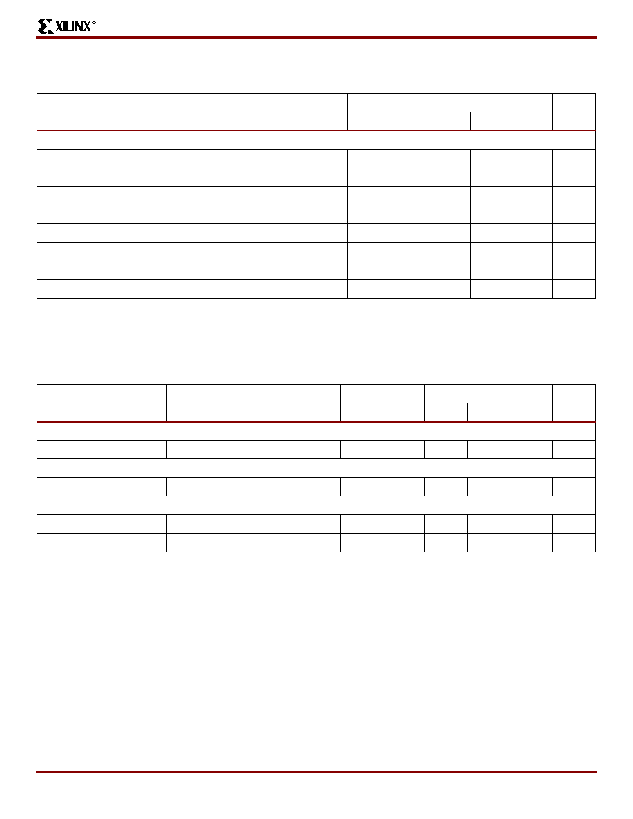
VirtexTM-II Platform FPGAs: DC and Switching Characteristics
R
DS031-3 (v3.1) October 14, 2003
www.xilinx.com
Module 3 of 4
Product Specification
1-800-255-7778
32
Output Clock Jitter
Output Clock Phase Alignment
Table 37: Output Clock Jitter
Description
Symbol
Constraints
Speed Grade
Units
-6
-5
-4
Clock Synthesis Period Jitter
CLK0
CLKOUT_PER_JITT_0
±100
±100
±100
ps
CLK90
CLKOUT_PER_JITT_90
±150
±150
±150
ps
CLK180
CLKOUT_PER_JITT_180
±150
±150
±150
ps
CLK270
CLKOUT_PER_JITT_270
±150
±150
±150
ps
CLK2X, CLK2X180
CLKOUT_PER_JITT_2X
±200
±200
±200
ps
CLKDV (integer division)
CLKOUT_PER_JITT_DV1
±150
±150
±150
ps
CLKDV (non-integer division)
CLKOUT_PER_JITT_DV2
±300
±300
±300
ps
CLKFX, CLKFX180
CLKOUT_PER_JITT_FX
Note 1
Note 1
Note 1
ps
Notes:
1.
Values for this parameter are available at
www.xilinx.com
.
Table 38: Output Clock Phase Alignment
Description
Symbol
Constraints
Speed Grade
Units
-6
-5
-4
Phase Offset Between CLKIN and CLKFB
CLKIN/CLKFB
CLKIN_CLKFB_PHASE
±50
±50
±50
ps
Phase Offset Between Any DCM Outputs
All CLK outputs
CLKOUT_PHASE
±140
±140
±140
ps
Duty Cycle Precision
DLL outputs
(1)
CLKOUT_DUTY_CYCLE_DLL
(2)
±150
±150
±150
ps
CLKFX outputs
CLKOUT_DUTY_CYCLE_FX
±100
±100
±100
ps
Notes:
1.
"DLL outputs" is used here to describe the outputs: CLK0, CLK90, CLK180, CLK270, CLK2X, CLK2X180, and CLKDV.
2.
CLKOUT_DUTY_CYCLE_DLL applies to the 1X clock outputs (CLK0, CLK90, CLK180, and CLK270) only if
DUTY_CYCLE_CORRECTION = TRUE.
3.
Specification also applies to PSCLK.
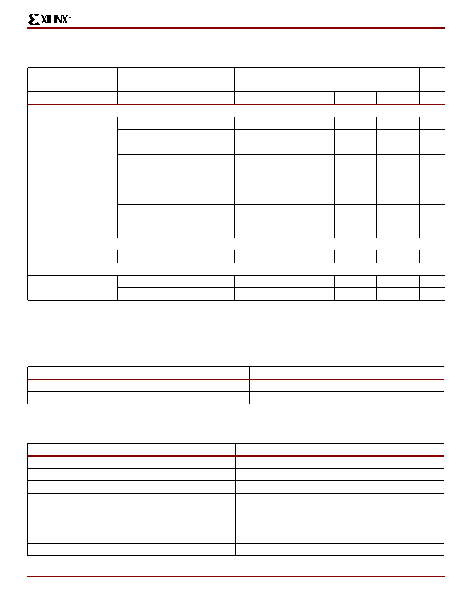
VirtexTM-II Platform FPGAs: DC and Switching Characteristics
R
DS031-3 (v3.1) October 14, 2003
www.xilinx.com
Module 3 of 4
Product Specification
1-800-255-7778
33
Miscellaneous Timing Parameters
Frequency Synthesis
Parameter Cross Reference
Table 39: Miscellaneous Timing Parameters
Description
Symbol
Constraints
F
CLKIN
Speed Grade
Units
-6
-5
-4
Time Required to Achieve LOCK
Using DLL outputs
(1)
LOCK_DLL
LOCK_DLL_60
> 60MHz
20.0
20.0
20.0
µs
LOCK_DLL_50_60
50 - 60 MHz
25.0
25.0
25.0
µs
LOCK_DLL_40_50
40 - 50 MHz
50.0
50.0
50.0
µs
LOCK_DLL_30_40
30 - 40 MHz
90.0
90.0
90.0
µs
LOCK_DLL_24_30
24 - 30 MHz
120.0
120.0
120.0
µs
Using CLKFX outputs
LOCK_FX_MIN
10.0
10.0
10.0
ms
LOCK_FX_MAX
10.0
10.0
10.0
ms
Additional lock time with
fine-phase shifting
LOCK_DLL_FINE_SHIFT
50.0
50.0
50.0
µs
Fine-Phase Shifting
Absolute shifting range
FINE_SHIFT_RANGE
10.0
10.0
10.0
ns
Delay Lines
Tap delay resolution
DCM_TAP_MIN
30.0
30.0
30.0
ps
DCM_TAP_MAX
60.0
60.0
60.0
ps
Notes:
1.
"DLL outputs" is used here to describe the outputs: CLK0, CLK90, CLK180, CLK270, CLK2X, CLK2X180, and CLKDV.
2.
Specification also applies to PSCLK.
Table 40: Frequency Synthesis
Attribute
Min
Max
CLKFX_MULTIPLY
2
32
CLKFX_DIVIDE
1
32
Table 41: Parameter Cross Reference
Libraries Guide
Data Sheet
DLL_CLKOUT_{MIN|MAX}_LF
CLKOUT_FREQ_{1X|2X|DV}_LF
DFS_CLKOUT_{MIN|MAX}_LF
CLKOUT_FREQ_FX_LF
DLL_CLKIN_{MIN|MAX}_LF
CLKIN_FREQ_DLL_LF
DFS_CLKIN_{MIN|MAX}_LF
CLKIN_FREQ_FX_LF
DLL_CLKOUT_{MIN|MAX}_HF
CLKOUT_FREQ_{1X|DV}_HF
DFS_CLKOUT_{MIN|MAX}_HF
CLKOUT_FREQ_FX_HF
DLL_CLKIN_{MIN|MAX}_HF
CLKIN_FREQ_DLL_HF
DFS_CLKIN_{MIN|MAX}_HF
CLKIN_FREQ_FX_HF

VirtexTM-II Platform FPGAs: DC and Switching Characteristics
R
DS031-3 (v3.1) October 14, 2003
www.xilinx.com
Module 3 of 4
Product Specification
1-800-255-7778
34
Source-Synchronous Switching Characteristics
The parameters in this section provide the necessary values for calculating timing budgets for Virtex-II source-synchronous
transmitter and receiver data-valid windows.
Table 42: Duty Cycle Distortion and Clock-Tree Skew
Description
Symbol
Device
Speed Grade
Units
-6
-5
-4
Duty Cycle Distortion
(1)
T
DCD_CLK0
All
140
140
140
ps
T
DCD_CLK180
All
50
50
50
ps
Clock Tree Skew
(2)
T
CKSKEW
XC2V40
50
50
60
ps
XC2V80
50
50
60
ps
XC2V250
50
50
60
ps
XC2V500
50
50
60
ps
XC2V1000
80
80
90
ps
XC2V1500
80
80
90
ps
XC2V2000
100
100
110
ps
XC2V3000
100
100
110
ps
XC2V4000
400
400
450
ps
XC2V6000
500
500
550
ps
XC2V8000
600
650
ps
Notes:
1.
These parameters represent the worst-case duty cycle distortion observable at the pins of the device using LVDS output buffers. For
cases where other I/O standards are used, IBIS can be used to calculate any additional duty cycle distortion that might be caused
by asymmetrical rise/fall times.
T
DCD_CLK0
applies to cases where local (IOB) inversion is used to provide the negative-edge clock to the DDR element in the I/O.
T
DCD_CLK180
applies to cases where the CLK180 output of the DCM is used to provide the negative-edge clock to the DDR element
in the I/O.
2.
This value represents the worst-case clock-tree skew observable between sequential I/O elements. Significantly less clock-tree skew
exists for I/O registers that are close to each other and fed by the same or adjacent clock-tree branches. Use the Xilinx FPGA_Editor
and Timing Analyzer tools to evaluate clock skew specific to your application.
Table 43: Package Skew
Description
Symbol
Device/Package
Value
Units
Package Skew
(1)
T
PKGSKEW
XC2V1000 / FF896
130
ps
XC2V3000 / FF1152
115
ps
XC2V3000 / BF957
130
ps
XC2V4000 / FF1152
130
ps
XC2V4000 / FF1517
200
ps
XC2V4000 / BF957
140
ps
XC2V6000 / FF1152
90
ps
XC2V6000 / FF1517
105
ps
XC2V6000 / BF957
105
ps
Notes:
1.
These values represent the worst-case skew between any two balls of the package: shortest flight time to longest flight time from Pad
to Ball (7.1ps per mm).
2.
Package trace length information is available for these device/package combinations. This information can be used to deskew the
package.

VirtexTM-II Platform FPGAs: DC and Switching Characteristics
R
DS031-3 (v3.1) October 14, 2003
www.xilinx.com
Module 3 of 4
Product Specification
1-800-255-7778
35
Table 44: Sample Window
Description
Symbol
Device
Speed Grade
Units
-6
-5
-4
Sampling Error at Receiver Pins
(1)
T
SAMP
XC2V40
500
500
550
ps
XC2V80
500
500
550
ps
XC2V250
500
500
550
ps
XC2V500
500
500
550
ps
XC2V1000
500
500
550
ps
XC2V1500
500
500
550
ps
XC2V2000
500
500
550
ps
XC2V3000
500
500
550
ps
XC2V4000
500
500
550
ps
XC2V6000
500
500
550
ps
XC2V8000
500
550
ps
Notes:
1.
This parameter indicates the total sampling error of Virtex-II
DDR input registers across voltage, temperature, and process. The
characterization methodology uses the DCM to capture the DDR input registers' edges of operation. These measurements include:
- CLK0 and CLK180 DCM jitter
- Worst-case Duty-Cycle Distortion - T
DCD_CLK180
- DCM accuracy (phase offset)
- DCM phase shift resolution.
These measurements do not include package or clock tree skew.
Table 45: Pin-to-Pin Setup/Hold: Source-Synchronous Configuration
Description
Symbol
Device
Speed Grade
Units
-6
-5
-4
Data Input Set-Up and Hold Times Relative to a Forwarded
Clock Input Pin, Using DCM and Global Clock Buffer.
For situations where clock and data inputs conform to
different standards, adjust the setup and hold values
accordingly using the values shown in
IOB Input Switching
Characteristics Standard Adjustments, page 11
.
No Delay
Global Clock and IFF with DCM
T
PSDCM
/
T
PHDCM
XC2V40
0.2/0.5
0.2/0.5
0.2/0.5
ns
XC2V80
0.2/0.5
0.2/0.5
0.2/0.5
ns
XC2V250
0.2/0.5
0.2/0.5
0.2/0.5
ns
XC2V500
0.2/0.5
0.2/0.5
0.2/0.5
ns
XC2V1000
0.2/0.5
0.2/0.5
0.2/0.5
ns
XC2V1500
0.2/0.5
0.2/0.5
0.2/0.5
ns
XC2V2000
0.2/0.5
0.2/0.5
0.2/0.5
ns
XC2V3000
0.2/0.5
0.2/0.5
0.2/0.6
ns
XC2V4000
0.2/0.5
0.2/0.6
0.2/0.6
ns
XC2V6000
0.2/0.5
0.2/0.6
0.2/0.6
ns
XC2V8000
0.2/0.6
0.2/0.7
ns
Notes:
1.
IFF = Input Flip-Flop
2.
The timing values were measured using the fine-phase adjustment feature of the DCM.
3.
The worst-case duty-cycle distortion and DCM jitter on CLK0 and CLK180 is included in these measurements.
VirtexTM-II Platform FPGAs: DC and Switching Characteristics
R
DS031-3 (v3.1) October 14, 2003
www.xilinx.com
Module 3 of 4
Product Specification
1-800-255-7778
36
Source Synchronous Timing Budgets
This section describes how to use the parameters provided in the
Source-Synchronous Switching Characteristics
section to develop system-specific timing budgets. The following analysis provides information necessary for determining
Virtex-II contributions to an overall system timing analysis; no assumptions are made about the effects of Inter-Symbol
Interference or PCB skew.
Virtex-II Transmitter Data-Valid Window (T
X
)
T
X
is the minimum aggregate valid data period for a
source-synchronous data bus at the pins of the device and
is calculated as follows:
T
X
= Data Period - [Jitter
(1)
+ Duty Cycle Distortion
(2)
+
TCKSKEW
(3)
+ TPKGSKEW
(4)
]
Notes:
1.
Jitter values and accumulation methodology to be provided in
a future release of this document. The absolute period jitter
values found in the
DCM Timing Parameters
section of the
particular DCM output clock used to clock the IOB FF can be
used for a best case analysis.
2.
This value depends on the clocking methodology used. See
Note1 for
Table 42
.
3.
This value represents the worst-case clock-tree skew
observable between sequential I/O elements. Significantly
less clock-tree skew exists for I/O registers that are close to
each other and fed by the same or adjacent clock-tree
branches. Use the Xilinx FPGA_Editor and Timing Analyzer
tools to evaluate clock skew specific to your application.
4.
These values represent the worst-case skew between any two
balls of the package: shortest flight time to longest flight time
from Pad to Ball.
Virtex-II Receiver Data-Valid Window (R
X
)
R
X
is the required minimum aggregate valid data period for
a source-synchronous data bus at the pins of the device
and is calculated as follows:
R
X
= [TSAMP
(1)
+ TCKSKEW
(2)
+ TPKGSKEW
(3)
]
Notes:
1.
This parameter indicates the total sampling error of Virtex-II
DDR input registers across voltage, temperature, and
process. The characterization methodology uses the DCM to
capture the DDR input registers' edges of operation. These
measurements include:
-
CLK0 and CLK180 DCM jitter in a quiet system
-
Worst-case duty-cycle distortion
-
DCM accuracy (phase offset)
-
DCM phase shift resolution.
These measurements do not include package or clock tree
skew.
2.
This value represents the worst-case clock-tree skew
observable between sequential I/O elements. Significantly
less clock-tree skew exists for I/O registers that are close to
each other and fed by the same or adjacent clock-tree
branches. Use the Xilinx FPGA_Editor and Timing Analyzer
tools to evaluate clock skew specific to your application.
3.
These values represent the worst-case skew between any two
balls of the package: shortest flight time to longest flight time
from Pad to Ball.
Revision History
This section records the change history for this module of the data sheet.
Date
Version
Revision
11/07/00
1.0
Early access draft.
12/06/00
1.1
Initial release.
01/15/01
1.2
Added values to the tables in the
Virtex-II Performance Characteristics
and
Virtex-II
Switching Characteristics
sections.
01/25/01
1.3
∑
The data sheet was divided into four modules (per the current style standard).
∑
Updated values in the
Virtex-II Performance Characteristics
and
Virtex-II
Switching Characteristics
tables.
∑
Table 18, "Delay Measurement Methodology"
04/23/01
1.5
∑
Updated values in the
Virtex-II Performance Characteristics
and
Virtex-II
Switching Characteristics
tables.
∑
Added T
REG32
symbol to
Table 23
.
∑
Skipped v1.4 to sync with other modules. Reverted to traditional double-column
format.
VirtexTM-II Platform FPGAs: DC and Switching Characteristics
R
DS031-3 (v3.1) October 14, 2003
www.xilinx.com
Module 3 of 4
Product Specification
1-800-255-7778
37
07/30/01
1.6
∑
Updated values in the
Virtex-II Performance Characteristics
and
Virtex-II
Switching Characteristics
tables.
∑
Added values to the
Virtex-II Pin-to-Pin Output Parameter Guidelines
and
Virtex-II
Pin-to-Pin Input Parameter Guidelines
tables.
∑
Added
Frequency Synthesis
table.
10/02/01
1.7
∑
Updated values in the
Virtex-II Performance Characteristics
and
Virtex-II
Switching Characteristics
tables.
∑
Updated the speed grade designations used in data sheets, and added
Table 13
,
which shows the current speed grade designation for each device.
10/05/01
1.8
∑
Corrected the speed grade designation for the XC2V1000 device in
Table 13
.
10/12/01
1.9
∑
Updated values in the
Virtex-II Performance Characteristics
and
Virtex-II
Switching Characteristics
tables.
11/28/01
2.0
∑
Updated values in
Table 3
,
Table 4
,
Table 5
,
Virtex-II Performance Characteristics
,
and
Virtex-II Switching Characteristics
tables.
01/03/02
2.1
∑
Updated values in
Virtex-II Performance Characteristics
and
Virtex-II Switching
Characteristics
tables, based on values extracted from speedsfile version 1.96.
∑
Changed the speed grade designation for the XC2V6000 device in
Table 13
.
07/16/02
2.2
∑
Updated values in
Table 4
, "
Quiescent Supply Current
."
∑
Updated values in
Virtex-II Performance Characteristics
and
Virtex-II Switching
Characteristics
tables, based on values extracted from speedsfile version 1.111.
∑
Added
Enhanced Multiplier Switching Characteristics
section.
∑
Added footnote to
Table 34
, "
Global Clock Setup and Hold for LVTTL Standard,
Without DCM
."
∑
Added
Source-Synchronous Switching Characteristics
section.
09/26/02
2.3
∑
Removed mention of MIL-M-38510/605 specification.
∑
Added footnotes to
Table 2
and
Table 6
.
12/06/02
2.4
∑
Revised SSTL2 values in
Table 6
to match the latest JEDEC specification.
∑
Added footnote regarding V
IN
PCI compliance to
Table 1
.
∑
Added footnote regarding
CLKOUT_DUTY_CYCLE_DLL
to
Table 38
.
05/07/03
2.5
∑
Updated values in
Virtex-II Performance Characteristics
and
Virtex-II Switching
Characteristics
tables, based on values extracted from speedsfile version 1.114.
∑
Table 4
,
Quiescent Supply Current
, and
Table 5
,
Minimum Power On Current
Required for Virtex-II Devices
: Added parameters for XC2V8000 device.
∑
Table 16
,
IOB Output Switching Characteristics
: Changed parameter designator
T
IOTON
to T
IOTP
.
∑
Table 26
,
Enhanced Multiplier Switching Characteristics
: Corrected all parameter
designators from T
MULT_P[nn]
to T
MULT1_P[nn]
in order to correspond with designators
used in speedsfile.
∑
Table 27
,
Enhanced Pipelined Multiplier Switching Characteristics
: Corrected all
parameter designators from T
MULTCK_P[nn]
to T
MULTCK1_P[nn]
in order to correspond
with designators used in speedsfile.
∑
Removed old Table 19, Standard Capacitive Loads.
∑
Added Figure 1, page 17, showing test configuration for measuring I/O standard
adjustments.
06/19/03
2.5.1
∑
Removed footnotes in
Table 31
and
Table 33
that stated DCM jitter was included in the
measurements.
Date
Version
Revision
VirtexTM-II Platform FPGAs: DC and Switching Characteristics
R
DS031-3 (v3.1) October 14, 2003
www.xilinx.com
Module 3 of 4
Product Specification
1-800-255-7778
38
Virtex-II Data Sheet
The Virtex-II Data Sheet contains the following modules:
∑
VirtexTM-II Platform FPGAs: Introduction and Overview
(Module 1)
∑
VirtexTM-II Platform FPGAs: Detailed Description
(Module 2)
∑
VirtexTM-II Platform FPGAs: DC and Switching
Characteristics (Module 3)
∑
VirtexTM-II Platform FPGAs: Pinout Information
(Module 4)
08/01/03
3.0
∑
Table 13
: All Virtex-II devices and speed grades now Production.
∑
Updated values in
Virtex-II Performance Characteristics
and
Virtex-II Switching
Characteristics
tables, based on values extracted from speedsfile version 1.116.
∑
Table 31
and
Table 32
: Revised test setup footnote to refer to
Figure 1
. Previously
specified a capacitive load parameter.
∑
Figure 1: Added note to figure regarding termination resistors.
10/14/03
3.1
∑
Table 1
: Changed T
J
description from "Operating junction temperature" to "Maximum
junction temperature".
∑
In section
General Power Supply Requirements
, replaced reference to Answer
Record 11713 with reference to
XAPP689
regarding handling of simultaneously
switching outputs (SSO).
∑
In section
I/O Standard Adjustment Measurement Methodology
:
-
Table 18
renamed
Input Delay Measurement Methodology
. Added footnotes.
-
Added new
Table 19
,
Output Delay Measurement Methodology
.
-
Replaced
Figure 1
,
Generalized Test Setup
, with new drawing.
-
Revised and extended text describing output delay measurement procedure.
∑
Table 42
,
Table 44
, and
Table 45
: All Source-Synchronous parameters for all devices
now available in these tables.
∑
XC2V8000 is no longer offered in the -6 speed grade. The following tables containing
parameters or other references to this device/grade combination were corrected
accordingly:
Table 13
,
Table 14
,
Table 31
,
Table 32
,
Table 33
,
Table 34
,
Table 42
,
Table 44
, and
Table 45
.
∑
Table 36
: For Input Clock Low/High Pulse Width, PSCLK and CLKIN, changed existing
Footnote (2) to new Footnote (3).
Date
Version
Revision
© 2001-2002 Xilinx, Inc. All rights reserved. All Xilinx trademarks, registered trademarks, patents, and disclaimers are as listed at
http://www.xilinx.com/legal.htm
.
All other trademarks and registered trademarks are the property of their respective owners. All specifications are subject to change without notice.
DS031-4 (v2.0) August 1, 2003
www.xilinx.com
Module 4 of 4
Product Specification
1-800-255-7778
1
This document provides
Virtex-II Device/Package Combi-
nations and Maximum I/Os Available
and
Virtex-II Pin
Definitions
, followed by pinout tables for the following pack-
ages:
∑
CS144 Chip-Scale BGA Package
∑
FG256 Fine-Pitch BGA Package
∑
FG456 Fine-Pitch BGA Package
∑
FG676 Fine-Pitch BGA Package
∑
BG575 Standard BGA Package
∑
BG728 Standard BGA Package
∑
FF896 Flip-Chip Fine-Pitch BGA Package
∑
FF1152 Flip-Chip Fine-Pitch BGA Package
∑
FF1517 Flip-Chip Fine-Pitch BGA Package
∑
BF957 Flip-Chip BGA Package
For device pinout diagrams and layout guidelines, refer to
the
Virtex-II Platform FPGA User Guide
. ASCII package
pinout files are also available for download from the Xilinx
website (
www.xilinx.com
).
Virtex-II Device/Package Combinations
and Maximum I/Os Available
Wire-bond and flip-chip packages are available.
Table 1
and
Table 2
show the maximum number of user I/Os possible in
wire-bond and flip-chip packages, respectively.
Table 3
shows the number of user I/Os available for all
device/package combinations.
∑
CS denotes wire-bond chip-scale ball grid array (BGA)
(0.80 mm pitch).
∑
FG denotes wire-bond fine-pitch BGA (1.00 mm pitch).
∑
FF denotes flip-chip fine-pitch BGA (1.00 mm pitch).
∑
BG denotes standard BGA (1.27 mm pitch).
∑
BF denotes flip-chip BGA (1.27 mm pitch).
The number of I/Os per package include all user I/Os except
the 15 control pins (CCLK, DONE, M0, M1, M2, PROG_B,
PWRDWN_B, TCK, TDI, TDO, TMS, HSWAP_EN, DXN,
DXP, AND RSVD).
0
225
VirtexTM-II Platform FPGAs:
Pinout Information
DS031-4 (v2.0) August 1, 2003
0
0
Product Specification
R
Table 1: Wire-Bond Packages Information
Package
CS144
FG256
FG456
FG676
BG575
BG728
Pitch (mm)
0.80
1.00
1.00
1.00
1.27
1.27
Size (mm)
12 x 12
17 x 17
23 x 23
27 x 27
31 x 31
35 x 35
I/Os
92
172
324
484
408
516
Table 2: Flip-Chip Packages Information
Package
FF896
FF1152
FF1517
BF957
Pitch (mm)
1.00
1.00
1.00
1.27
Size (mm)
31 x 31
35 x 35
40 x 40
40 x 40
I/Os
624
824
1,108
684

VirtexTM-II Platform FPGAs: Pinout Information
R
DS031-4 (v2.0) August 1, 2003
www.xilinx.com
Module 4 of 4
Product Specification
1-800-255-7778
2
Virtex-II
Pin Definitions
This section describes the pinouts for Virtex-II devices in the
following packages:
∑
CS144: wire-bond chip-scale ball grid array (BGA) of
0.80 mm pitch
∑
FG256, FG456, and FG676: wire-bond fine-pitch BGA
of 1.00 mm pitch
∑
FF896, FF1152, FF1517: flip-chip fine-pitch BGA of
1.00 mm pitch
∑
BG575 and BG728: wire-bond BGA of 1.27 mm pitch
∑
BF957: flip-chip BGA of 1.27 mm pitch
All of the devices supported in a particular package are
pinout compatible and are listed in the same table (one
table per package). In addition, the FG456 and FG676
packages are compatible, as are the FF896 and FF1152
packages. Pins that are not available for the smallest
devices are listed in right-hand columns.
Each device is split into eight I/O banks to allow for flexibility
in the choice of I/O standards (see the Virtex-II Data Sheet).
Global pins, including JTAG, configuration, and
power/ground pins, are listed at the end of each table.
Table 4
provides definitions for all pin types.
The FG256 pinouts (
Table 6
) is included as an example. All
Virtex-II pinout tables are available on the distribution
CD-ROM, or on the web (at
http://www.xilinx.com
).
Table 3: Virtex-II Device/Package Combinations and Maximum Number of Available I/Os
Package
Available I/Os
XC2V
40
XC2V
80
XC2V
250
XC2V
500
XC2V
1000
XC2V
1500
XC2V
2000
XC2V
3000
XC2V
4000
XC2V
6000
XC2V
8000
CS144
88
92
92
-
-
-
-
-
-
-
-
FG256
88
120
172
172
172
-
-
-
-
-
-
FG456
-
-
200
264
324
-
-
-
-
-
-
FG676
-
-
-
-
-
392
456
484
-
-
-
FF896
-
-
-
-
432
528
624
-
-
-
-
FF1152
-
-
-
-
-
-
-
720
824
824
824
FF1517
-
-
-
-
-
-
-
-
912
1,104
1,108
BG575
-
-
-
-
328
392
408
-
-
-
-
BG728
-
-
-
-
-
-
-
516
-
-
-
BF957
-
-
-
-
-
-
624
684
684
684
-

VirtexTM-II Platform FPGAs: Pinout Information
R
DS031-4 (v2.0) August 1, 2003
www.xilinx.com
Module 4 of 4
Product Specification
1-800-255-7778
3
Pin Definitions
Table 4
provides a description of each pin type listed in Virtex-II pinout tables.
Table 4: Virtex-II Pin Definitions
Pin Name
Direction
Description
User I/O Pins
IO_LXXY_#
Input/Output
All user I/O pins are capable of differential signalling and can implement LVDS, ULVDS,
BLVDS, LVPECL, or LDT pairs. Each user I/O is labeled "IO_LXXY_#", where:
IO indicates a user I/O pin.
LXXY indicates a differential pair, with XX a unique pair in the bank and Y = P/N for
the positive and negative sides of the differential pair.
# indicates the bank number (0 through 7)
Dual-Function Pins
IO_LXXY_#/ZZZ
The dual-function pins are labelled "IO_LXXY_#/ZZZ", where ZZZ can be one of the
following pins:
Per Bank - VRP, VRN, or VREF
Globally - GCLKX(S/P), BUSY/DOUT, INIT_B, D0/DIN ≠ D7, RDWR_B, or CS_B
With /ZZZ:
D0/DIN, D1, D2,
D3, D4, D5, D6,
D7
Input/Output
∑
In SelectMAP mode, D0 through D7 are configuration data pins. These pins
become user I/Os after configuration, unless the SelectMAP port is retained.
∑
In bit-serial modes, DIN (D0) is the single-data input. This pin becomes a user I/O
after configuration.
CS_B
Input
In SelectMAP mode, this is the active-low Chip Select signal. The pin becomes a user
I/O after configuration, unless the SelectMAP port is retained.
RDWR_B
Input
In SelectMAP mode, this is the active-low Write Enable signal. The pin becomes a user
I/O after configuration, unless the SelectMAP port is retained.
BUSY/DOUT
Output
∑
In SelectMAP mode, BUSY controls the rate at which configuration data is loaded.
The pin becomes a user I/O after configuration, unless the SelectMAP port is
retained.
∑
In bit-serial modes, DOUT provides preamble and configuration data to
downstream devices in a daisy-chain. The pin becomes a user I/O after
configuration.
INIT_B
Bidirectional
(open-drain)
When Low, this pin indicates that the configuration memory is being cleared. When held
Low, the start of configuration is delayed. During configuration, a Low on this output
indicates that a configuration data error has occurred. The pin becomes a user I/O after
configuration.
GCLKx (S/P)
Input/Output
These are clock input pins that connect to Global Clock Buffers. These pins become
regular user I/Os when not needed for clocks.
VRP
Input
This pin is for the DCI voltage reference resistor of P transistor (per bank).
VRN
Input
This pin is for the DCI voltage reference resistor of N transistor (per bank).
ALT_VRP
Input
This is the alternative pin for the DCI voltage reference resistor of P transistor.
ALT_VRN
Input
This is the alternative pin for the DCI voltage reference resistor of N transistor.
V
REF
Input
These are input threshold voltage pins. They become user I/Os when an external
threshold voltage is not needed (per bank).
Dedicated Pins
(1)
VirtexTM-II Platform FPGAs: Pinout Information
R
DS031-4 (v2.0) August 1, 2003
www.xilinx.com
Module 4 of 4
Product Specification
1-800-255-7778
4
CCLK
Input/Output
Configuration clock. Output in Master mode or Input in Slave mode.
PROG_B
Input
Active Low asynchronous reset to configuration logic. This pin has a permanent weak
pull-up resistor.
DONE
Input/Output
DONE is a bidirectional signal with an optional internal pull-up resistor. As an output,
this pin indicates completion of the configuration process. As an input, a Low level on
DONE can be configured to delay the start-up sequence.
M2, M1, M0
Input
Configuration mode selection.
HSWAP_EN
Input
Enable I/O pullups during configuration.
TCK
Input
Boundary Scan Clock.
TDI
Input
Boundary Scan Data Input.
TDO
Output
Boundary Scan Data Output.
TMS
Input
Boundary Scan Mode Select.
PWRDWN_B
Input
(unsupported)
Active Low power-down pin (unsupported). Driving this pin Low can adversely affect
device operation and configuration. PWRDWN_B is internally pulled High, which is its
default state. It does not require an external pull-up.
Other Pins
DXN, DXP
N/A
Temperature-sensing diode pins (Anode: DXP, Cathode: DXN).
V
BATT
Input
Decryptor key memory backup supply. (Do not connect if battery is not used.)
RSVD
N/A
Reserved pin - do not connect.
V
CCO
Input
Power-supply pins for the output drivers (per bank).
V
CCAUX
Input
Power-supply pins for auxiliary circuits.
V
CCINT
Input
Power-supply pins for the internal core logic.
GND
Input
Ground.
Notes:
1.
All dedicated pins (JTAG and configuration) are powered by V
CCAUX
(independent of the bank V
CCO
voltage).
Table 4: Virtex-II Pin Definitions (Continued)
Pin Name
Direction
Description
VirtexTM-II Platform FPGAs: Pinout Information
R
DS031-4 (v2.0) August 1, 2003
www.xilinx.com
Module 4 of 4
Product Specification
1-800-255-7778
5
CS144 Chip-Scale BGA Package
As shown in
Table 5
, XC2V40, XC2V80, and XC2V250 Virtex-II devices are available in the CS144 package. Pins in the
XC2V40, XC2V80, and XC2V250 devices are the same except for pin differences in the XC2V40 device, shown in the No
Connect column. Following this table are the
CS144 Chip-Scale BGA Package Specifications (0.80mm pitch)
.
Table 5: CS144 -- XC2V40, XC2V80, and XC2V250
Bank
Pin Description
Pin Number
No Connect in the XC2V40
0
IO_L01N_0
B3
0
IO_L01P_0
A3
0
IO_L02N_0
C4
0
IO_L02P_0
B4
0
IO_L03N_0/VRP_0
A4
0
IO_L03P_0/VRN_0
D5
0
IO_L94N_0/VREF_0
A5
0
IO_L94P_0
D6
0
IO_L95N_0/GCLK7P
C6
0
IO_L95P_0/GCLK6S
B6
0
IO_L96N_0/GCLK5P
A6
0
IO_L96P_0/GCLK4S
D7
1
IO_L96N_1/GCLK3P
A7
1
IO_L96P_1/GCLK2S
B7
1
IO_L95N_1/GCLK1P
A8
1
IO_L95P_1/GCLK0S
B8
1
IO_L94N_1
C8
1
IO_L94P_1/VREF_1
D8
1
IO_L03N_1/VRP_1
C9
1
IO_L03P_1/VRN_1
D9
1
IO_L02N_1
A10
1
IO_L02P_1
B10
1
IO_L01N_1
C10
1
IO_L01P_1
D10
2
IO_L01N_2
C13
2
IO_L01P_2
D11
2
IO_L02N_2/VRP_2
D12
2
IO_L02P_2/VRN_2
D13
2
IO_L03N_2
E10
2
IO_L03P_2/VREF_2
E11
2
IO_L93N_2
E13
NC
2
IO_L93P_2/VREF_2
F11
NC
2
IO_L94N_2
F12
2
IO_L94P_2
G10
VirtexTM-II Platform FPGAs: Pinout Information
R
DS031-4 (v2.0) August 1, 2003
www.xilinx.com
Module 4 of 4
Product Specification
1-800-255-7778
6
2
IO_L96N_2
G11
2
IO_L96P_2
G13
3
IO_L96N_3
G12
3
IO_L96P_3
H12
3
IO_L94N_3
H11
3
IO_L94P_3
J13
3
IO_L03N_3/VREF_3
J10
3
IO_L03P_3
K13
3
IO_L02N_3/VRP_3
K12
3
IO_L02P_3/VRN_3
K11
3
IO_L01N_3
K10
3
IO_L01P_3
L13
4
IO_L01N_4/BUSY/DOUT
(1)
M11
4
IO_L01P_4/INIT_B
N11
4
IO_L02N_4/D0/DIN
(1)
L10
4
IO_L02P_4/D1
M10
4
IO_L03N_4/D2/ALT_VRP_4
N10
4
IO_L03P_4/D3/ALT_VRN_4
K9
4
IO_L94N_4/VREF_4
N9
4
IO_L94P_4
K8
4
IO_L95N_4/GCLK3S
L8
4
IO_L95P_4/GCLK2P
M8
4
IO_L96N_4/GCLK1S
N8
4
IO_L96P_4/GCLK0P
K7
5
IO_L96N_5/GCLK7S
N7
5
IO_L96P_5/GCLK6P
M7
5
IO_L95N_5/GCLK5S
N6
5
IO_L95P_5/GCLK4P
M6
5
IO_L94N_5
L6
5
IO_L94P_5/VREF_5
K6
5
IO_L03N_5/D4/ALT_VRP_5
L5
5
IO_L03P_5/D5/ALT_VRN_5
K5
5
IO_L02N_5/D6
N4
5
IO_L02P_5/D7
M4
5
IO_L01N_5/RDWR_B
L4
5
IO_L01P_5/CS_B
K4
Table 5: CS144 -- XC2V40, XC2V80, and XC2V250
Bank
Pin Description
Pin Number
No Connect in the XC2V40
VirtexTM-II Platform FPGAs: Pinout Information
R
DS031-4 (v2.0) August 1, 2003
www.xilinx.com
Module 4 of 4
Product Specification
1-800-255-7778
7
6
IO_L01P_6
L3
6
IO_L01N_6
L2
6
IO_L02P_6/VRN_6
L1
6
IO_L02N_6/VRP_6
K3
6
IO_L03P_6
K2
6
IO_L03N_6/VREF_6
K1
6
IO_L94P_6
J2
6
IO_L94N_6
H4
6
IO_L96P_6
H3
6
IO_L96N_6
H1
7
IO_L96P_7
G4
7
IO_L96N_7
G3
7
IO_L94P_7
G1
7
IO_L94N_7
F1
7
IO_L93P_7/VREF_7
F2
NC
7
IO_L93N_7
F4
NC
7
IO_L03P_7/VREF_7
E2
7
IO_L03N_7
E3
7
IO_L02P_7/VRN_7
E4
7
IO_L02N_7/VRP_7
D1
7
IO_L01P_7
D2
7
IO_L01N_7
D3
0
VCCO_0
B5
0
VCCO_0
C3
1
VCCO_1
A11
1
VCCO_1
A9
2
VCCO_2
F10
2
VCCO_2
C12
3
VCCO_3
L12
3
VCCO_3
J12
4
VCCO_4
M9
4
VCCO_4
L11
5
VCCO_5
N3
5
VCCO_5
N5
6
VCCO_6
J3
6
VCCO_6
M1
7
VCCO_7
D4
7
VCCO_7
F3
Table 5: CS144 -- XC2V40, XC2V80, and XC2V250
Bank
Pin Description
Pin Number
No Connect in the XC2V40

VirtexTM-II Platform FPGAs: Pinout Information
R
DS031-4 (v2.0) August 1, 2003
www.xilinx.com
Module 4 of 4
Product Specification
1-800-255-7778
8
NA
CCLK
M13
NA
PROG_B
B1
NA
DONE
N12
NA
M0
N2
NA
M1
M2
NA
M2
M3
NA
TCK
B12
NA
TDI
C1
NA
TDO
C11
NA
TMS
A13
NA
PWRDWN_B
M12
NA
HSWAP_EN
A1
NA
RSVD
A2
NA
RSVD
B2
NA
VBATT
A12
NA
RSVD
B11
NA
VCCAUX
C2
NA
VCCAUX
N1
NA
VCCAUX
N13
NA
VCCAUX
B13
NA
VCCINT
H2
NA
VCCINT
L7
NA
VCCINT
H13
NA
VCCINT
C7
NA
GND
E1
NA
GND
G2
NA
GND
J1
NA
GND
J4
NA
GND
M5
NA
GND
L9
NA
GND
J11
NA
GND
H10
NA
GND
F13
NA
GND
E12
NA
GND
B9
NA
GND
C5
Notes:
1.
See
Table 4
for an explanation of the signals available on this pin.
Table 5: CS144 -- XC2V40, XC2V80, and XC2V250
Bank
Pin Description
Pin Number
No Connect in the XC2V40
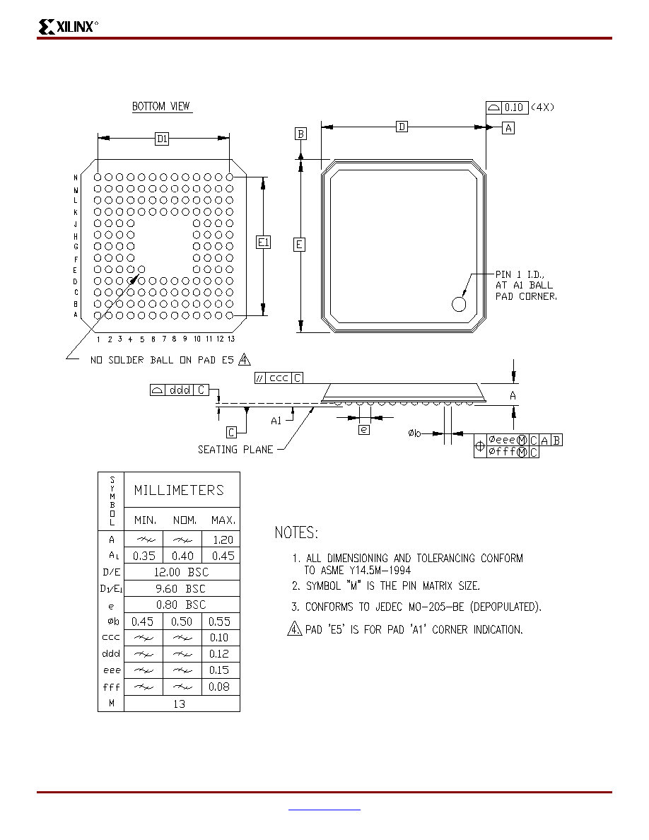
VirtexTM-II Platform FPGAs: Pinout Information
R
DS031-4 (v2.0) August 1, 2003
www.xilinx.com
Module 4 of 4
Product Specification
1-800-255-7778
9
CS144 Chip-Scale BGA Package Specifications (0.80mm pitch)
Figure 1: CS144 Chip-Scale BGA Package Specifications
VirtexTM-II Platform FPGAs: Pinout Information
R
DS031-4 (v2.0) August 1, 2003
www.xilinx.com
Module 4 of 4
Product Specification
1-800-255-7778
10
FG256 Fine-Pitch BGA Package
As shown in
Table 6
, XC2V40, XC2V80, XC2V250, XC2V500, and XC2V1000 Virtex-II devices are available in the FG256
fine-pitch BGA package. The pins in the XC2V250, XC2V500, and XC2V1000 devices are same. The No Connect columns
show pin differences for the XC2V40 and XC2V80 devices. Following this table are the
FG256 Fine-Pitch BGA Package
Specifications (1.00mm pitch)
.
Table 6: FG256 BGA -- XC2V40, XC2V80, XC2V250, XC2V500, and XC2V1000
Bank
Pin Description
Pin Number
No Connect in XC2V40
No Connect in XC2V80
0
IO_L01N_0
C4
0
IO_L01P_0
B4
0
IO_L02N_0
D5
0
IO_L02P_0
C5
0
IO_L03N_0/VRP_0
B5
0
IO_L03P_0/VRN_0
A5
0
IO_L04N_0/VREF_0
D6
NC
NC
0
IO_L04P_0
C6
NC
NC
0
IO_L05N_0
B6
NC
NC
0
IO_L05P_0
A6
NC
NC
0
IO_L92N_0
E6
NC
NC
0
IO_L92P_0
E7
NC
NC
0
IO_L93N_0
D7
NC
NC
0
IO_L93P_0
C7
NC
NC
0
IO_L94N_0/VREF_0
B7
0
IO_L94P_0
A7
0
IO_L95N_0/GCLK7P
D8
0
IO_L95P_0/GCLK6S
C8
0
IO_L96N_0/GCLK5P
B8
0
IO_L96P_0/GCLK4S
A8
1
IO_L96N_1/GCLK3P
A9
1
IO_L96P_1/GCLK2S
B9
1
IO_L95N_1/GCLK1P
C9
1
IO_L95P_1/GCLK0S
D9
1
IO_L94N_1
A10
1
IO_L94P_1/VREF_1
B10
1
IO_L93N_1
C10
NC
NC
1
IO_L93P_1
D10
NC
NC
1
IO_L92N_1
E10
NC
NC

VirtexTM-II Platform FPGAs: Pinout Information
R
DS031-4 (v2.0) August 1, 2003
www.xilinx.com
Module 4 of 4
Product Specification
1-800-255-7778
11
1
IO_L92P_1
E11
NC
NC
1
IO_L05N_1
A11
NC
NC
1
IO_L05P_1
B11
NC
NC
1
IO_L04N_1
C11
NC
NC
1
IO_L04P_1/VREF_1
D11
NC
NC
1
IO_L03N_1/VRP_1
A12
1
IO_L03P_1/VRN_1
B12
1
IO_L02N_1
C12
1
IO_L02P_1
D12
1
IO_L01N_1
B13
1
IO_L01P_1
C13
2
IO_L01N_2
C16
2
IO_L01P_2
D16
2
IO_L02N_2/VRP_2
D14
2
IO_L02P_2/VRN_2
D15
2
IO_L03N_2
E13
2
IO_L03P_2/VREF_2
E14
2
IO_L04N_2
E15
NC
2
IO_L04P_2
E16
NC
2
IO_L06N_2
F13
NC
2
IO_L06P_2
F14
NC
2
IO_L43N_2
F15
NC
NC
2
IO_L43P_2
F16
NC
NC
2
IO_L45N_2
F12
NC
NC
2
IO_L45P_2/VREF_2
G12
NC
NC
2
IO_L91N_2
G13
NC
2
IO_L91P_2
G14
NC
2
IO_L93N_2
G15
NC
2
IO_L93P_2/VREF_2
G16
NC
2
IO_L94N_2
H13
2
IO_L94P_2
H14
2
IO_L96N_2
H15
2
IO_L96P_2
H16
Table 6: FG256 BGA -- XC2V40, XC2V80, XC2V250, XC2V500, and XC2V1000
Bank
Pin Description
Pin Number
No Connect in XC2V40
No Connect in XC2V80
VirtexTM-II Platform FPGAs: Pinout Information
R
DS031-4 (v2.0) August 1, 2003
www.xilinx.com
Module 4 of 4
Product Specification
1-800-255-7778
12
3
IO_L96N_3
J16
3
IO_L96P_3
J15
3
IO_L94N_3
J14
3
IO_L94P_3
J13
3
IO_L93N_3/VREF_3
K16
NC
3
IO_L93P_3
K15
NC
3
IO_L91N_3
K14
NC
3
IO_L91P_3
K13
NC
3
IO_L45N_3/VREF_3
K12
NC
NC
3
IO_L45P_3
L12
NC
NC
3
IO_L43N_3
L16
NC
NC
3
IO_L43P_3
L15
NC
NC
3
IO_L06N_3
L14
NC
3
IO_L06P_3
L13
NC
3
IO_L04N_3
M16
NC
3
IO_L04P_3
M15
NC
3
IO_L03N_3/VREF_3
M14
3
IO_L03P_3
M13
3
IO_L02N_3/VRP_3
N15
3
IO_L02P_3/VRN_3
N14
3
IO_L01N_3
N16
3
IO_L01P_3
P16
4
IO_L01N_4/BUSY/DOUT
(1)
T14
4
IO_L01P_4/INIT_B
T13
4
IO_L02N_4/D0/DIN
(1)
P13
4
IO_L02P_4/D1
R13
4
IO_L03N_4/D2/ALT_VRP_4
N12
4
IO_L03P_4/D3/ALT_VRN_4
P12
4
IO_L04N_4/VREF_4
R12
NC
NC
4
IO_L04P_4
T12
NC
NC
4
IO_L05N_4/VRP_4
N11
NC
NC
4
IO_L05P_4/VRN_4
P11
NC
NC
Table 6: FG256 BGA -- XC2V40, XC2V80, XC2V250, XC2V500, and XC2V1000
Bank
Pin Description
Pin Number
No Connect in XC2V40
No Connect in XC2V80
VirtexTM-II Platform FPGAs: Pinout Information
R
DS031-4 (v2.0) August 1, 2003
www.xilinx.com
Module 4 of 4
Product Specification
1-800-255-7778
13
4
IO_L91N_4/VREF_4
R11
NC
NC
4
IO_L91P_4
T11
NC
NC
4
IO_L92N_4
M11
NC
NC
4
IO_L92P_4
M10
NC
NC
4
IO_L93N_4
N10
NC
NC
4
IO_L93P_4
P10
NC
NC
4
IO_L94N_4/VREF_4
R10
4
IO_L94P_4
T10
4
IO_L95N_4/GCLK3S
N9
4
IO_L95P_4/GCLK2P
P9
4
IO_L96N_4/GCLK1S
R9
4
IO_L96P_4/GCLK0P
T9
5
IO_L96N_5/GCLK7S
T8
5
IO_L96P_5/GCLK6P
R8
5
IO_L95N_5/GCLK5S
P8
5
IO_L95P_5/GCLK4P
N8
5
IO_L94N_5
T7
5
IO_L94P_5/VREF_5
R7
5
IO_L93N_5
P7
NC
NC
5
IO_L93P_5
N7
NC
NC
5
IO_L92N_5
M7
NC
NC
5
IO_L92P_5
M6
NC
NC
5
IO_L91N_5
T6
NC
NC
5
IO_L91P_5/VREF_5
R6
NC
NC
5
IO_L05N_5/VRP_5
P6
NC
NC
5
IO_L05P_5/VRN_5
N6
NC
NC
5
IO_L04N_5
T5
NC
NC
5
IO_L04P_5/VREF_5
R5
NC
NC
5
IO_L03N_5/D4/ALT_VRP_5
P5
5
IO_L03P_5/D5/ALT_VRN_5
N5
5
IO_L02N_5/D6
R4
5
IO_L02P_5/D7
P4
5
IO_L01N_5/RDWR_B
T4
Table 6: FG256 BGA -- XC2V40, XC2V80, XC2V250, XC2V500, and XC2V1000
Bank
Pin Description
Pin Number
No Connect in XC2V40
No Connect in XC2V80
VirtexTM-II Platform FPGAs: Pinout Information
R
DS031-4 (v2.0) August 1, 2003
www.xilinx.com
Module 4 of 4
Product Specification
1-800-255-7778
14
5
IO_L01P_5/CS_B
T3
6
IO_L01P_6
P1
6
IO_L01N_6
N1
6
IO_L02P_6/VRN_6
N3
6
IO_L02N_6/VRP_6
N2
6
IO_L03P_6
M4
6
IO_L03N_6/VREF_6
M3
6
IO_L04P_6
M2
NC
6
IO_L04N_6
M1
NC
6
IO_L06P_6
L4
NC
6
IO_L06N_6
L3
NC
6
IO_L43P_6
L2
NC
NC
6
IO_L43N_6
L1
NC
NC
6
IO_L45P_6
L5
NC
NC
6
IO_L45N_6/VREF_6
K5
NC
NC
6
IO_L91P_6
K4
NC
6
IO_L91N_6
K3
NC
6
IO_L93P_6
K2
NC
6
IO_L93N_6/VREF_6
K1
NC
6
IO_L94P_6
J4
6
IO_L94N_6
J3
6
IO_L96P_6
J2
6
IO_L96N_6
J1
7
IO_L96P_7
H1
7
IO_L96N_7
H2
7
IO_L94P_7
H3
7
IO_L94N_7
H4
7
IO_L93P_7/VREF_7
G1
NC
7
IO_L93N_7
G2
NC
7
IO_L91P_7
G3
NC
7
IO_L91N_7
G4
NC
7
IO_L45P_7/VREF_7
G5
NC
NC
Table 6: FG256 BGA -- XC2V40, XC2V80, XC2V250, XC2V500, and XC2V1000
Bank
Pin Description
Pin Number
No Connect in XC2V40
No Connect in XC2V80

VirtexTM-II Platform FPGAs: Pinout Information
R
DS031-4 (v2.0) August 1, 2003
www.xilinx.com
Module 4 of 4
Product Specification
1-800-255-7778
15
7
IO_L45N_7
F5
NC
NC
7
IO_L43P_7
F1
NC
NC
7
IO_L43N_7
F2
NC
NC
7
IO_L06P_7
F3
NC
7
IO_L06N_7
F4
NC
7
IO_L04P_7
E1
NC
7
IO_L04N_7
E2
NC
7
IO_L03P_7/VREF_7
E3
7
IO_L03N_7
E4
7
IO_L02P_7/VRN_7
D2
7
IO_L02N_7/VRP_7
D3
7
IO_L01P_7
D1
7
IO_L01N_7
C1
0
VCCO_0
F8
0
VCCO_0
F7
0
VCCO_0
E8
1
VCCO_1
F10
1
VCCO_1
F9
1
VCCO_1
E9
2
VCCO_2
H12
2
VCCO_2
H11
2
VCCO_2
G11
3
VCCO_3
K11
3
VCCO_3
J12
3
VCCO_3
J11
4
VCCO_4
M9
4
VCCO_4
L10
4
VCCO_4
L9
5
VCCO_5
M8
5
VCCO_5
L8
5
VCCO_5
L7
6
VCCO_6
K6
6
VCCO_6
J6
Table 6: FG256 BGA -- XC2V40, XC2V80, XC2V250, XC2V500, and XC2V1000
Bank
Pin Description
Pin Number
No Connect in XC2V40
No Connect in XC2V80
VirtexTM-II Platform FPGAs: Pinout Information
R
DS031-4 (v2.0) August 1, 2003
www.xilinx.com
Module 4 of 4
Product Specification
1-800-255-7778
16
6
VCCO_6
J5
7
VCCO_7
H6
7
VCCO_7
H5
7
VCCO_7
G6
NA
CCLK
P15
NA
PROG_B
A2
NA
DONE
R14
NA
M0
T2
NA
M1
P2
NA
M2
R3
NA
HSWAP_EN
B3
NA
TCK
A15
NA
TDI
C2
NA
TDO
C15
NA
TMS
B14
NA
PWRDWN_B
T15
NA
RSVD
A4
NA
RSVD
A3
NA
VBATT
A14
NA
RSVD
A13
NA
VCCAUX
R16
NA
VCCAUX
R1
NA
VCCAUX
B16
NA
VCCAUX
B1
NA
VCCINT
N13
NA
VCCINT
N4
NA
VCCINT
M12
NA
VCCINT
M5
NA
VCCINT
E12
NA
VCCINT
E5
NA
VCCINT
D13
NA
VCCINT
D4
Table 6: FG256 BGA -- XC2V40, XC2V80, XC2V250, XC2V500, and XC2V1000
Bank
Pin Description
Pin Number
No Connect in XC2V40
No Connect in XC2V80

VirtexTM-II Platform FPGAs: Pinout Information
R
DS031-4 (v2.0) August 1, 2003
www.xilinx.com
Module 4 of 4
Product Specification
1-800-255-7778
17
NA
GND
T16
NA
GND
T1
NA
GND
R15
NA
GND
R2
NA
GND
P14
NA
GND
P3
NA
GND
L11
NA
GND
L6
NA
GND
K10
NA
GND
K9
NA
GND
K8
NA
GND
K7
NA
GND
J10
NA
GND
J9
NA
GND
J8
NA
GND
J7
NA
GND
H10
NA
GND
H9
NA
GND
H8
NA
GND
H7
NA
GND
G10
NA
GND
G9
NA
GND
G8
NA
GND
G7
NA
GND
F11
NA
GND
F6
NA
GND
C14
NA
GND
C3
NA
GND
B15
NA
GND
B2
NA
GND
A16
NA
GND
A1
Notes:
1.
See
Table 4
for an explanation of the signals available on this pin.
Table 6: FG256 BGA -- XC2V40, XC2V80, XC2V250, XC2V500, and XC2V1000
Bank
Pin Description
Pin Number
No Connect in XC2V40
No Connect in XC2V80
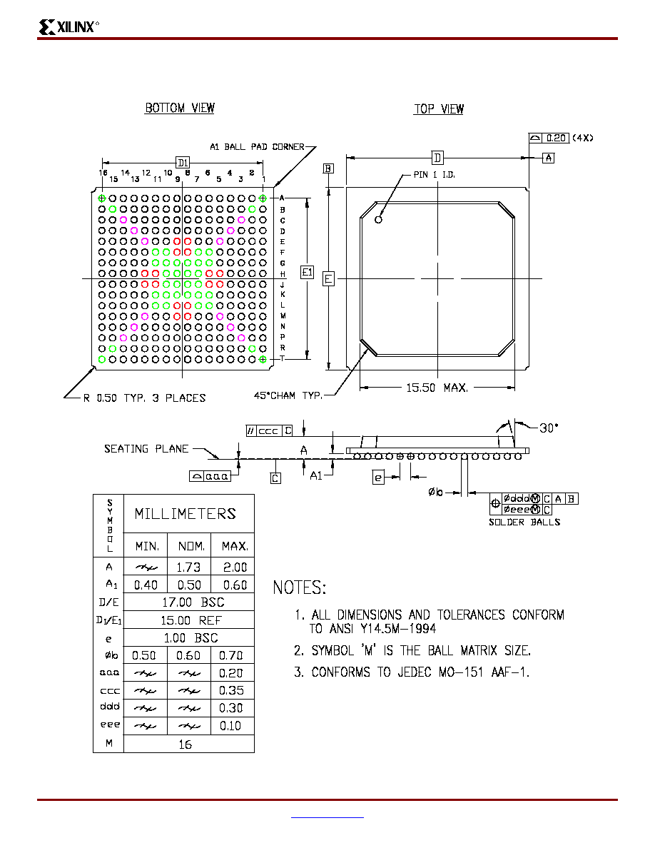
VirtexTM-II Platform FPGAs: Pinout Information
R
DS031-4 (v2.0) August 1, 2003
www.xilinx.com
Module 4 of 4
Product Specification
1-800-255-7778
18
FG256 Fine-Pitch BGA Package Specifications (1.00mm pitch)
Figure 2: FG256 Fine-Pitch BGA Package Specifications

VirtexTM-II Platform FPGAs: Pinout Information
R
DS031-4 (v2.0) August 1, 2003
www.xilinx.com
Module 4 of 4
Product Specification
1-800-255-7778
19
FG456 Fine-Pitch BGA Package
As shown in
Table 7
, XC2V250, XC2V500, and XC2V1000 Virtex-II devices are available in the FG456 fine-pitch BGA
package. Pins in the XC2V250, XC2V500, and XC2V1000 devices are the same, except for the pin differences in the
XC2V250 and XC2V500 devices shown in the No Connect columns. Following this table are the
FG456 Fine-Pitch BGA
Package Specifications (1.00mm pitch)
.
Table 7: FG456 BGA -- XC2V250, XC2V500, and XC2V1000
Bank
Pin Description
Pin Number
No Connect in XC2V250
No Connect in XC2V500
0
IO_L01N_0
B4
0
IO_L01P_0
A4
0
IO_L02N_0
C4
0
IO_L02P_0
C5
0
IO_L03N_0/VRP_0
B5
0
IO_L03P_0/VRN_0
A5
0
IO_L04N_0/VREF_0
D6
0
IO_L04P_0
C6
0
IO_L05N_0
B6
0
IO_L05P_0
A6
0
IO_L06N_0
E7
0
IO_L06P_0
E8
0
IO_L21N_0
D7
NC
NC
0
IO_L21P_0/VREF_0
C7
NC
NC
0
IO_L22N_0
B7
NC
NC
0
IO_L22P_0
A7
NC
NC
0
IO_L24N_0
D8
NC
NC
0
IO_L24P_0
C8
NC
NC
0
IO_L49N_0
B8
NC
0
IO_L49P_0
A8
NC
0
IO_L51N_0
E9
NC
0
IO_L51P_0/VREF_0
F9
NC
0
IO_L52N_0
D9
NC
0
IO_L52P_0
C9
NC
0
IO_L54N_0
B9
NC
0
IO_L54P_0
A9
NC
0
IO_L91N_0/VREF_0
E10
0
IO_L91P_0
F10
0
IO_L92N_0
D10
0
IO_L92P_0
C10
VirtexTM-II Platform FPGAs: Pinout Information
R
DS031-4 (v2.0) August 1, 2003
www.xilinx.com
Module 4 of 4
Product Specification
1-800-255-7778
20
0
IO_L93N_0
B10
0
IO_L93P_0
A10
0
IO_L94N_0/VREF_0
E11
0
IO_L94P_0
F11
0
IO_L95N_0/GCLK7P
D11
0
IO_L95P_0/GCLK6S
C11
0
IO_L96N_0/GCLK5P
B11
0
IO_L96P_0/GCLK4S
A11
1
IO_L96N_1/GCLK3P
F12
1
IO_L96P_1/GCLK2S
F13
1
IO_L95N_1/GCLK1P
E12
1
IO_L95P_1/GCLK0S
D12
1
IO_L94N_1
C12
1
IO_L94P_1/VREF_1
B12
1
IO_L93N_1
A13
1
IO_L93P_1
B13
1
IO_L92N_1
C13
1
IO_L92P_1
D13
1
IO_L91N_1
E13
1
IO_L91P_1/VREF_1
E14
1
IO_L54N_1
A14
NC
1
IO_L54P_1
B14
NC
1
IO_L52N_1
C14
NC
1
IO_L52P_1
D14
NC
1
IO_L51N_1/VREF_1
A15
NC
1
IO_L51P_1
B15
NC
1
IO_L49N_1
C15
NC
1
IO_L49P_1
D15
NC
1
IO_L24N_1
F14
NC
NC
1
IO_L24P_1
E15
NC
NC
1
IO_L22N_1
A16
NC
NC
1
IO_L22P_1
B16
NC
NC
1
IO_L21N_1/VREF_1
C16
NC
NC
Table 7: FG456 BGA -- XC2V250, XC2V500, and XC2V1000
Bank
Pin Description
Pin Number
No Connect in XC2V250
No Connect in XC2V500
VirtexTM-II Platform FPGAs: Pinout Information
R
DS031-4 (v2.0) August 1, 2003
www.xilinx.com
Module 4 of 4
Product Specification
1-800-255-7778
21
1
IO_L21P_1
D16
NC
NC
1
IO_L06N_1
E16
1
IO_L06P_1
E17
1
IO_L05N_1
A17
1
IO_L05P_1
B17
1
IO_L04N_1
C17
1
IO_L04P_1/VREF_1
D17
1
IO_L03N_1/VRP_1
A18
1
IO_L03P_1/VRN_1
B18
1
IO_L02N_1
C18
1
IO_L02P_1
D18
1
IO_L01N_1
A19
1
IO_L01P_1
B19
2
IO_L01N_2
C21
2
IO_L01P_2
C22
2
IO_L02N_2/VRP_2
E18
2
IO_L02P_2/VRN_2
F18
2
IO_L03N_2
D21
2
IO_L03P_2/VREF_2
D22
2
IO_L04N_2
E19
2
IO_L04P_2
E20
2
IO_L06N_2
E21
2
IO_L06P_2
E22
2
IO_L19N_2
F19
NC
NC
2
IO_L19P_2
F20
NC
NC
2
IO_L21N_2
F21
NC
NC
2
IO_L21P_2/VREF_2
F22
NC
NC
2
IO_L22N_2
G18
NC
NC
2
IO_L22P_2
H18
NC
NC
2
IO_L24N_2
G19
NC
NC
2
IO_L24P_2
G20
NC
NC
2
IO_L43N_2
G21
2
IO_L43P_2
G22
Table 7: FG456 BGA -- XC2V250, XC2V500, and XC2V1000
Bank
Pin Description
Pin Number
No Connect in XC2V250
No Connect in XC2V500
VirtexTM-II Platform FPGAs: Pinout Information
R
DS031-4 (v2.0) August 1, 2003
www.xilinx.com
Module 4 of 4
Product Specification
1-800-255-7778
22
2
IO_L45N_2
H19
2
IO_L45P_2/VREF_2
H20
2
IO_L46N_2
H21
2
IO_L46P_2
H22
2
IO_L48N_2
J17
2
IO_L48P_2
J18
2
IO_L49N_2
J19
NC
2
IO_L49P_2
J20
NC
2
IO_L51N_2
J21
NC
2
IO_L51P_2/VREF_2
J22
NC
2
IO_L52N_2
K17
NC
2
IO_L52P_2
K18
NC
2
IO_L54N_2
K19
NC
2
IO_L54P_2
K20
NC
2
IO_L91N_2
K21
2
IO_L91P_2
K22
2
IO_L93N_2
L17
2
IO_L93P_2/VREF_2
L18
2
IO_L94N_2
L19
2
IO_L94P_2
L20
2
IO_L96N_2
L21
2
IO_L96P_2
L22
3
IO_L96N_3
M21
3
IO_L96P_3
M20
3
IO_L94N_3
M19
3
IO_L94P_3
M18
3
IO_L93N_3/VREF_3
M17
3
IO_L93P_3
N17
3
IO_L91N_3
N22
3
IO_L91P_3
N21
3
IO_L54N_3
N20
NC
3
IO_L54P_3
N19
NC
3
IO_L52N_3
N18
NC
Table 7: FG456 BGA -- XC2V250, XC2V500, and XC2V1000
Bank
Pin Description
Pin Number
No Connect in XC2V250
No Connect in XC2V500

VirtexTM-II Platform FPGAs: Pinout Information
R
DS031-4 (v2.0) August 1, 2003
www.xilinx.com
Module 4 of 4
Product Specification
1-800-255-7778
23
3
IO_L52P_3
P18
NC
3
IO_L51N_3/VREF_3
P22
NC
3
IO_L51P_3
P21
NC
3
IO_L49N_3
P20
NC
3
IO_L49P_3
P19
NC
3
IO_L48N_3
R22
3
IO_L48P_3
R21
3
IO_L46N_3
R20
3
IO_L46P_3
R19
3
IO_L45N_3/VREF_3
R18
3
IO_L45P_3
P17
3
IO_L43N_3
T22
3
IO_L43P_3
T21
3
IO_L24N_3
T20
NC
NC
3
IO_L24P_3
T19
NC
NC
3
IO_L22N_3
U22
NC
NC
3
IO_L22P_3
U21
NC
NC
3
IO_L21N_3/VREF_3
U20
NC
NC
3
IO_L21P_3
U19
NC
NC
3
IO_L19N_3
T18
NC
NC
3
IO_L19P_3
U18
NC
NC
3
IO_L06N_3
V22
3
IO_L06P_3
V21
3
IO_L04N_3
V20
3
IO_L04P_3
V19
3
IO_L03N_3/VREF_3
W22
3
IO_L03P_3
W21
3
IO_L02N_3/VRP_3
Y22
3
IO_L02P_3/VRN_3
Y21
3
IO_L01N_3
W20
3
IO_L01P_3
AA20
4
IO_L01N_4/BUSY/DOUT
(1)
AB19
4
IO_L01P_4/INIT_B
AA19
Table 7: FG456 BGA -- XC2V250, XC2V500, and XC2V1000
Bank
Pin Description
Pin Number
No Connect in XC2V250
No Connect in XC2V500

VirtexTM-II Platform FPGAs: Pinout Information
R
DS031-4 (v2.0) August 1, 2003
www.xilinx.com
Module 4 of 4
Product Specification
1-800-255-7778
24
4
IO_L02N_4/D0/DIN
(1)
V18
4
IO_L02P_4/D1
V17
4
IO_L03N_4/D2/ALT_VRP_4
W18
4
IO_L03P_4/D3/ALT_VRN_4
Y18
4
IO_L04N_4/VREF_4
AA18
4
IO_L04P_4
AB18
4
IO_L05N_4/VRP_4
W17
4
IO_L05P_4/VRN_4
Y17
4
IO_L06N_4
AA17
4
IO_L06P_4
AB17
4
IO_L19N_4
V16
NC
NC
4
IO_L19P_4
V15
NC
NC
4
IO_L21N_4
W16
NC
NC
4
IO_L21P_4/VREF_4
Y16
NC
NC
4
IO_L22N_4
AA16
NC
NC
4
IO_L22P_4
AB16
NC
NC
4
IO_L24N_4
W15
NC
NC
4
IO_L24P_4
Y15
NC
NC
4
IO_L49N_4
AA15
NC
4
IO_L49P_4
AB15
NC
4
IO_L51N_4
U14
NC
4
IO_L51P_4/VREF_4
V14
NC
4
IO_L52N_4
W14
NC
4
IO_L52P_4
Y14
NC
4
IO_L54N_4
AA14
NC
4
IO_L54P_4
AB14
NC
4
IO_L91N_4/VREF_4
U13
4
IO_L91P_4
V13
4
IO_L92N_4
W13
4
IO_L92P_4
Y13
4
IO_L93N_4
AA13
4
IO_L93P_4
AB13
4
IO_L94N_4/VREF_4
U12
4
IO_L94P_4
V12
Table 7: FG456 BGA -- XC2V250, XC2V500, and XC2V1000
Bank
Pin Description
Pin Number
No Connect in XC2V250
No Connect in XC2V500
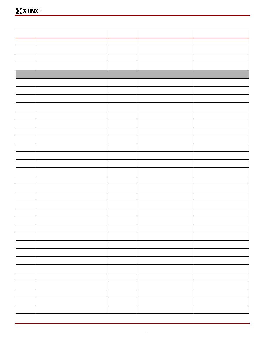
VirtexTM-II Platform FPGAs: Pinout Information
R
DS031-4 (v2.0) August 1, 2003
www.xilinx.com
Module 4 of 4
Product Specification
1-800-255-7778
25
4
IO_L95N_4/GCLK3S
W12
4
IO_L95P_4/GCLK2P
Y12
4
IO_L96N_4/GCLK1S
AA12
4
IO_L96P_4/GCLK0P
AB12
5
IO_L96N_5/GCLK7S
AA11
5
IO_L96P_5/GCLK6P
Y11
5
IO_L95N_5/GCLK5S
W11
5
IO_L95P_5/GCLK4P
V11
5
IO_L94N_5
U11
5
IO_L94P_5/VREF_5
U10
5
IO_L93N_5
AB10
5
IO_L93P_5
AA10
5
IO_L92N_5
Y10
5
IO_L92P_5
W10
5
IO_L91N_5
V10
5
IO_L91P_5/VREF_5
V9
5
IO_L54N_5
AB9
NC
5
IO_L54P_5
AA9
NC
5
IO_L52N_5
Y9
NC
5
IO_L52P_5
W9
NC
5
IO_L51N_5/VREF_5
AB8
NC
5
IO_L51P_5
AA8
NC
5
IO_L49N_5
Y8
NC
5
IO_L49P_5
W8
NC
5
IO_L24N_5
U9
NC
NC
5
IO_L24P_5
V8
NC
NC
5
IO_L22N_5
AB7
NC
NC
5
IO_L22P_5
AA7
NC
NC
5
IO_L21N_5/VREF_5
Y7
NC
NC
5
IO_L21P_5
W7
NC
NC
5
IO_L19N_5
AB6
NC
NC
5
IO_L19P_5
AA6
NC
NC
5
IO_L06N_5
Y6
Table 7: FG456 BGA -- XC2V250, XC2V500, and XC2V1000
Bank
Pin Description
Pin Number
No Connect in XC2V250
No Connect in XC2V500
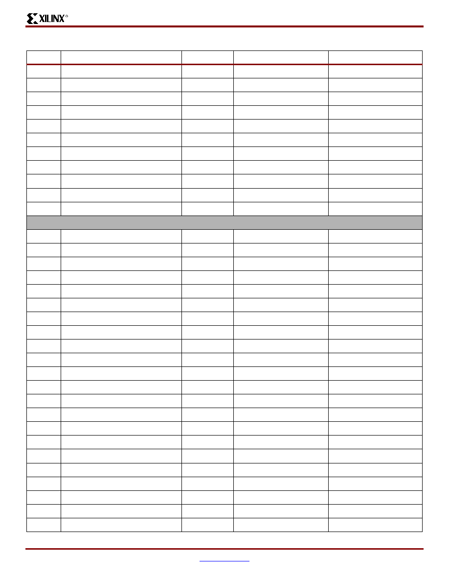
VirtexTM-II Platform FPGAs: Pinout Information
R
DS031-4 (v2.0) August 1, 2003
www.xilinx.com
Module 4 of 4
Product Specification
1-800-255-7778
26
5
IO_L06P_5
W6
5
IO_L05N_5/VRP_5
V7
5
IO_L05P_5/VRN_5
V6
5
IO_L04N_5
AB5
5
IO_L04P_5/VREF_5
AA5
5
IO_L03N_5/D4/ALT_VRP_5
Y5
5
IO_L03P_5/D5/ALT_VRN_5
W5
5
IO_L02N_5/D6
AB4
5
IO_L02P_5/D7
AA4
5
IO_L01N_5/RDWR_B
Y4
5
IO_L01P_5/CS_B
AA3
6
IO_L01P_6
V5
6
IO_L01N_6
U5
6
IO_L02P_6/VRN_6
Y2
6
IO_L02N_6/VRP_6
Y1
6
IO_L03P_6
V4
6
IO_L03N_6/VREF_6
V3
6
IO_L04P_6
W2
6
IO_L04N_6
W1
6
IO_L06P_6
U4
6
IO_L06N_6
U3
6
IO_L19P_6
V2
NC
NC
6
IO_L19N_6
V1
NC
NC
6
IO_L21P_6
U2
NC
NC
6
IO_L21N_6/VREF_6
U1
NC
NC
6
IO_L22P_6
T5
NC
NC
6
IO_L22N_6
R5
NC
NC
6
IO_L24P_6
T4
NC
NC
6
IO_L24N_6
T3
NC
NC
6
IO_L43P_6
T2
6
IO_L43N_6
T1
6
IO_L45P_6
R4
6
IO_L45N_6/VREF_6
R3
Table 7: FG456 BGA -- XC2V250, XC2V500, and XC2V1000
Bank
Pin Description
Pin Number
No Connect in XC2V250
No Connect in XC2V500

VirtexTM-II Platform FPGAs: Pinout Information
R
DS031-4 (v2.0) August 1, 2003
www.xilinx.com
Module 4 of 4
Product Specification
1-800-255-7778
27
6
IO_L46P_6
R2
6
IO_L46N_6
R1
6
IO_L48P_6
P6
6
IO_L48N_6
P5
6
IO_L49P_6
P4
NC
6
IO_L49N_6
P3
NC
6
IO_L51P_6
P2
NC
6
IO_L51N_6/VREF_6
P1
NC
6
IO_L52P_6
N6
NC
6
IO_L52N_6
N5
NC
6
IO_L54P_6
N4
NC
6
IO_L54N_6
N3
NC
6
IO_L91P_6
N2
6
IO_L91N_6
N1
6
IO_L93P_6
M6
6
IO_L93N_6/VREF_6
M5
6
IO_L94P_6
M4
6
IO_L94N_6
M3
6
IO_L96P_6
M2
6
IO_L96N_6
M1
7
IO_L96P_7
L2
7
IO_L96N_7
L3
7
IO_L94P_7
L4
7
IO_L94N_7
L5
7
IO_L93P_7/VREF_7
K1
7
IO_L93N_7
K2
7
IO_L91P_7
K3
7
IO_L91N_7
K4
7
IO_L54P_7
L6
NC
7
IO_L54N_7
K6
NC
7
IO_L52P_7
K5
NC
7
IO_L52N_7
J5
NC
7
IO_L51P_7/VREF_7
J1
NC
Table 7: FG456 BGA -- XC2V250, XC2V500, and XC2V1000
Bank
Pin Description
Pin Number
No Connect in XC2V250
No Connect in XC2V500
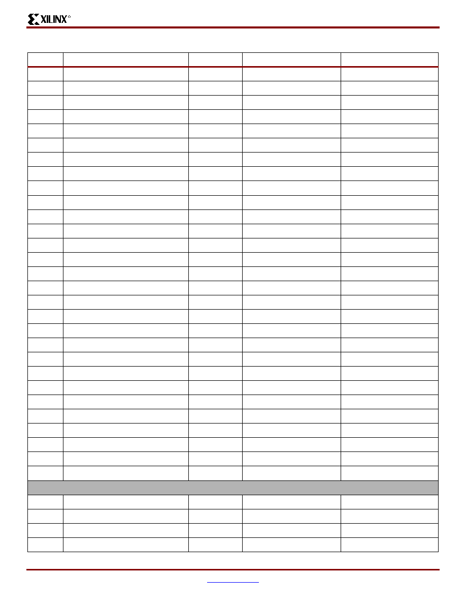
VirtexTM-II Platform FPGAs: Pinout Information
R
DS031-4 (v2.0) August 1, 2003
www.xilinx.com
Module 4 of 4
Product Specification
1-800-255-7778
28
7
IO_L51N_7
J2
NC
7
IO_L49P_7
J3
NC
7
IO_L49N_7
J4
NC
7
IO_L48P_7
H1
7
IO_L48N_7
H2
7
IO_L46P_7
H3
7
IO_L46N_7
H4
7
IO_L45P_7/VREF_7
J6
7
IO_L45N_7
H5
7
IO_L43P_7
G1
7
IO_L43N_7
G2
7
IO_L24P_7
G3
NC
NC
7
IO_L24N_7
G4
NC
NC
7
IO_L22P_7
F1
NC
NC
7
IO_L22N_7
F2
NC
NC
7
IO_L21P_7/VREF_7
F3
NC
NC
7
IO_L21N_7
F4
NC
NC
7
IO_L19P_7
G5
NC
NC
7
IO_L19N_7
F5
NC
NC
7
IO_L06P_7
E1
7
IO_L06N_7
E2
7
IO_L04P_7
E3
7
IO_L04N_7
E4
7
IO_L03P_7/VREF_7
D1
7
IO_L03N_7
D2
7
IO_L02P_7/VRN_7
C1
7
IO_L02N_7/VRP_7
C2
7
IO_L01P_7
E5
7
IO_L01N_7
E6
0
VCCO_0
G11
0
VCCO_0
G10
0
VCCO_0
G9
0
VCCO_0
F8
Table 7: FG456 BGA -- XC2V250, XC2V500, and XC2V1000
Bank
Pin Description
Pin Number
No Connect in XC2V250
No Connect in XC2V500

VirtexTM-II Platform FPGAs: Pinout Information
R
DS031-4 (v2.0) August 1, 2003
www.xilinx.com
Module 4 of 4
Product Specification
1-800-255-7778
29
0
VCCO_0
F7
1
VCCO_1
G14
1
VCCO_1
G13
1
VCCO_1
G12
1
VCCO_1
F16
1
VCCO_1
F15
2
VCCO_2
L16
2
VCCO_2
K16
2
VCCO_2
J16
2
VCCO_2
H17
2
VCCO_2
G17
3
VCCO_3
T17
3
VCCO_3
R17
3
VCCO_3
P16
3
VCCO_3
N16
3
VCCO_3
M16
4
VCCO_4
U16
4
VCCO_4
U15
4
VCCO_4
T14
4
VCCO_4
T13
4
VCCO_4
T12
5
VCCO_5
U8
5
VCCO_5
U7
5
VCCO_5
T11
5
VCCO_5
T10
5
VCCO_5
T9
6
VCCO_6
T6
6
VCCO_6
R6
6
VCCO_6
P7
6
VCCO_6
N7
6
VCCO_6
M7
7
VCCO_7
L7
7
VCCO_7
K7
7
VCCO_7
J7
Table 7: FG456 BGA -- XC2V250, XC2V500, and XC2V1000
Bank
Pin Description
Pin Number
No Connect in XC2V250
No Connect in XC2V500

VirtexTM-II Platform FPGAs: Pinout Information
R
DS031-4 (v2.0) August 1, 2003
www.xilinx.com
Module 4 of 4
Product Specification
1-800-255-7778
30
7
VCCO_7
H6
7
VCCO_7
G6
NA
CCLK
Y19
NA
PROG_B
A2
NA
DONE
AB20
NA
M0
AB2
NA
M1
W3
NA
M2
AB3
NA
HSWAP_EN
B3
NA
TCK
C19
NA
TDI
D3
NA
TDO
D20
NA
TMS
B20
NA
PWRDWN_B
AB21
NA
DXN
D5
NA
DXP
A3
NA
VBATT
A21
NA
RSVD
A20
NA
VCCAUX
AB11
NA
VCCAUX
AA22
NA
VCCAUX
AA1
NA
VCCAUX
M22
NA
VCCAUX
L1
NA
VCCAUX
B22
NA
VCCAUX
B1
NA
VCCAUX
A12
NA
VCCINT
U17
NA
VCCINT
U6
NA
VCCINT
T16
NA
VCCINT
T15
NA
VCCINT
T8
NA
VCCINT
T7
Table 7: FG456 BGA -- XC2V250, XC2V500, and XC2V1000
Bank
Pin Description
Pin Number
No Connect in XC2V250
No Connect in XC2V500
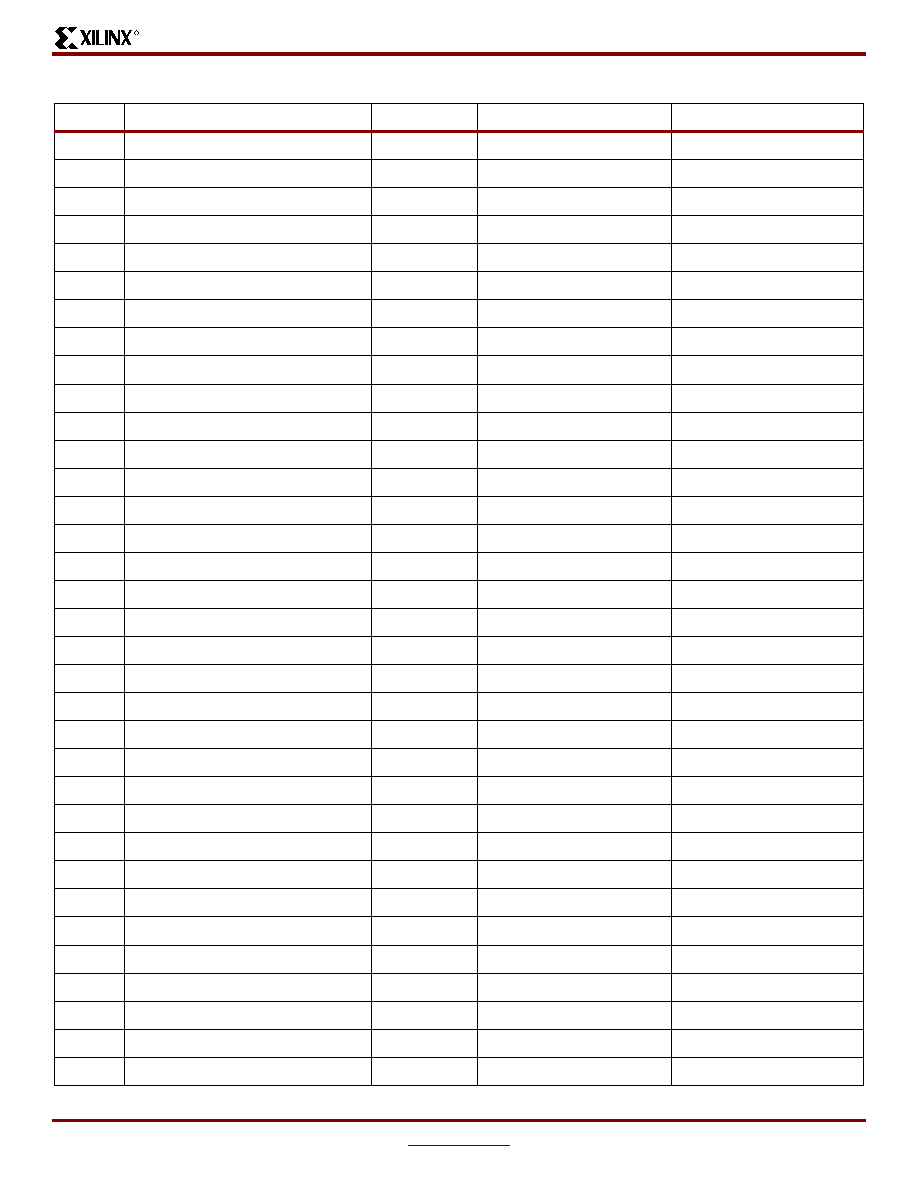
VirtexTM-II Platform FPGAs: Pinout Information
R
DS031-4 (v2.0) August 1, 2003
www.xilinx.com
Module 4 of 4
Product Specification
1-800-255-7778
31
NA
VCCINT
R16
NA
VCCINT
R7
NA
VCCINT
H16
NA
VCCINT
H7
NA
VCCINT
G16
NA
VCCINT
G15
NA
VCCINT
G8
NA
VCCINT
G7
NA
VCCINT
F17
NA
VCCINT
F6
NA
GND
AB22
NA
GND
AB1
NA
GND
AA21
NA
GND
AA2
NA
GND
Y20
NA
GND
Y3
NA
GND
W19
NA
GND
W4
NA
GND
P14
NA
GND
P13
NA
GND
P12
NA
GND
P11
NA
GND
P10
NA
GND
P9
NA
GND
N14
NA
GND
N13
NA
GND
N12
NA
GND
N11
NA
GND
N10
NA
GND
N9
NA
GND
M14
NA
GND
M13
NA
GND
M12
NA
GND
M11
Table 7: FG456 BGA -- XC2V250, XC2V500, and XC2V1000
Bank
Pin Description
Pin Number
No Connect in XC2V250
No Connect in XC2V500
VirtexTM-II Platform FPGAs: Pinout Information
R
DS031-4 (v2.0) August 1, 2003
www.xilinx.com
Module 4 of 4
Product Specification
1-800-255-7778
32
NA
GND
M10
NA
GND
M9
NA
GND
L14
NA
GND
L13
NA
GND
L12
NA
GND
L11
NA
GND
L10
NA
GND
L9
NA
GND
K14
NA
GND
K13
NA
GND
K12
NA
GND
K11
NA
GND
K10
NA
GND
K9
NA
GND
J14
NA
GND
J13
NA
GND
J12
NA
GND
J11
NA
GND
J10
NA
GND
J9
NA
GND
D19
NA
GND
D4
NA
GND
C20
NA
GND
C3
NA
GND
B21
NA
GND
B2
NA
GND
A22
NA
GND
A1
Notes:
1.
See
Table 4
for an explanation of the signals available on this pin.
Table 7: FG456 BGA -- XC2V250, XC2V500, and XC2V1000
Bank
Pin Description
Pin Number
No Connect in XC2V250
No Connect in XC2V500
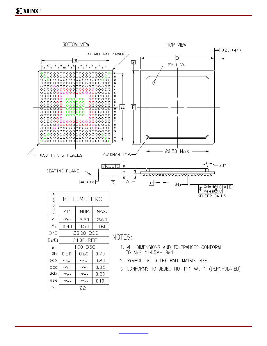
VirtexTM-II Platform FPGAs: Pinout Information
R
DS031-4 (v2.0) August 1, 2003
www.xilinx.com
Module 4 of 4
Product Specification
1-800-255-7778
33
FG456 Fine-Pitch BGA Package Specifications (1.00mm pitch)
Figure 3: FG456 Fine-Pitch BGA Package Specifications

VirtexTM-II Platform FPGAs: Pinout Information
R
DS031-4 (v2.0) August 1, 2003
www.xilinx.com
Module 4 of 4
Product Specification
1-800-255-7778
34
FG676 Fine-Pitch BGA Package
As shown in
Table 8
, XC2V1500, XC2V2000, and XC2V3000 Virtex-II devices are available in the FG676 fine-pitch BGA
package. Pins in the XC2V1500, XC2V2000, and XC2V3000 devices are the same, except for the pin differences in the
XC2V1500 and XC2V2000 devices shown in the No Connect columns. Following this table are the
FG676 Fine-Pitch BGA
Package Specifications (1.00mm pitch)
.
Table 8: FG676 BGA -- XC2V1500, XC2V2000, and XC2V3000
Bank
Pin Description
Pin Number
No Connect in XC2V1500
No Connect in XC2V2000
0
IO_L01N_0
D6
0
IO_L01P_0
C6
0
IO_L02N_0
B1
0
IO_L02P_0
A2
0
IO_L03N_0/VRP_0
D7
0
IO_L03P_0/VRN_0
C7
0
IO_L04N_0/VREF_0
B3
0
IO_L04P_0
A3
0
IO_L05N_0
G6
0
IO_L05P_0
G7
0
IO_L06N_0
E6
0
IO_L06P_0
E7
0
IO_L19N_0
B4
0
IO_L19P_0
A4
0
IO_L21N_0
B5
0
IO_L21P_0/VREF_0
A5
0
IO_L22N_0
B6
0
IO_L22P_0
A6
0
IO_L24N_0
A7
0
IO_L24P_0
A8
0
IO_L25N_0
E8
NC
NC
0
IO_L25P_0
D8
NC
NC
0
IO_L27N_0
G8
NC
NC
0
IO_L27P_0/VREF_0
F8
NC
NC
0
IO_L49N_0
C8
0
IO_L49P_0
B8
0
IO_L51N_0
D9
0
IO_L51P_0/VREF_0
E9
0
IO_L52N_0
F9
0
IO_L52P_0
G9
0
IO_L54N_0
B9
0
IO_L54P_0
A9
0
IO_L67N_0
C9
VirtexTM-II Platform FPGAs: Pinout Information
R
DS031-4 (v2.0) August 1, 2003
www.xilinx.com
Module 4 of 4
Product Specification
1-800-255-7778
35
0
IO_L67P_0
C10
0
IO_L69N_0
F10
0
IO_L69P_0/VREF_0
G10
0
IO_L70N_0
E10
0
IO_L70P_0
D10
0
IO_L72N_0
A10
0
IO_L72P_0
A11
0
IO_L73N_0
F11
NC
0
IO_L73P_0
E11
NC
0
IO_L75N_0
G11
NC
0
IO_L75P_0/VREF_0
H11
NC
0
IO_L76N_0
D11
NC
0
IO_L76P_0
C11
NC
0
IO_L78N_0
B11
NC
0
IO_L78P_0
B12
NC
0
IO_L91N_0/VREF_0
G12
0
IO_L91P_0
H12
0
IO_L92N_0
F12
0
IO_L92P_0
E12
0
IO_L93N_0
D12
0
IO_L93P_0
C12
0
IO_L94N_0/VREF_0
G13
0
IO_L94P_0
H13
0
IO_L95N_0/GCLK7P
F13
0
IO_L95P_0/GCLK6S
E13
0
IO_L96N_0/GCLK5P
D13
0
IO_L96P_0/GCLK4S
C13
1
IO_L96N_1/GCLK3P
H14
1
IO_L96P_1/GCLK2S
H15
1
IO_L95N_1/GCLK1P
G14
1
IO_L95P_1/GCLK0S
F14
1
IO_L94N_1
E14
1
IO_L94P_1/VREF_1
D14
1
IO_L93N_1
A12
1
IO_L93P_1
A13
1
IO_L92N_1
A14
Table 8: FG676 BGA -- XC2V1500, XC2V2000, and XC2V3000
Bank
Pin Description
Pin Number
No Connect in XC2V1500
No Connect in XC2V2000

VirtexTM-II Platform FPGAs: Pinout Information
R
DS031-4 (v2.0) August 1, 2003
www.xilinx.com
Module 4 of 4
Product Specification
1-800-255-7778
36
1
IO_L92P_1
A15
1
IO_L91N_1
B15
1
IO_L91P_1/VREF_1
C15
1
IO_L78N_1
D15
NC
1
IO_L78P_1
E15
NC
1
IO_L76N_1
F15
NC
1
IO_L76P_1
G15
NC
1
IO_L75N_1/VREF_1
G16
NC
1
IO_L75P_1
F16
NC
1
IO_L73N_1
A16
NC
1
IO_L73P_1
A17
NC
1
IO_L72N_1
B16
1
IO_L72P_1
C16
1
IO_L70N_1
D16
1
IO_L70P_1
E16
1
IO_L69N_1/VREF_1
C17
1
IO_L69P_1
D17
1
IO_L67N_1
H16
1
IO_L67P_1
G17
1
IO_L54N_1
E17
1
IO_L54P_1
F17
1
IO_L52N_1
A18
1
IO_L52P_1
A19
1
IO_L51N_1/VREF_1
E18
1
IO_L51P_1
D18
1
IO_L49N_1
B18
1
IO_L49P_1
C18
1
IO_L27N_1/VREF_1
F19
NC
NC
1
IO_L27P_1
F18
NC
NC
1
IO_L25N_1
G18
NC
NC
1
IO_L25P_1
G19
NC
NC
1
IO_L24N_1
B19
1
IO_L24P_1
C19
1
IO_L22N_1
D19
1
IO_L22P_1
E19
1
IO_L21N_1/VREF_1
A20
1
IO_L21P_1
A21
Table 8: FG676 BGA -- XC2V1500, XC2V2000, and XC2V3000
Bank
Pin Description
Pin Number
No Connect in XC2V1500
No Connect in XC2V2000

VirtexTM-II Platform FPGAs: Pinout Information
R
DS031-4 (v2.0) August 1, 2003
www.xilinx.com
Module 4 of 4
Product Specification
1-800-255-7778
37
1
IO_L19N_1
E20
1
IO_L19P_1
F20
1
IO_L06N_1
B21
1
IO_L06P_1
B22
1
IO_L05N_1
A22
1
IO_L05P_1
A23
1
IO_L04N_1
C21
1
IO_L04P_1/VREF_1
D21
1
IO_L03N_1/VRP_1
C20
1
IO_L03P_1/VRN_1
D20
1
IO_L02N_1
A24
1
IO_L02P_1
A25
1
IO_L01N_1
B23
1
IO_L01P_1
B24
2
IO_L01N_2
B26
2
IO_L01P_2
C26
2
IO_L02N_2/VRP_2
G20
2
IO_L02P_2/VRN_2
H20
2
IO_L03N_2
C25
2
IO_L03P_2/VREF_2
D25
2
IO_L04N_2
E23
2
IO_L04P_2
E24
2
IO_L06N_2
G21
2
IO_L06P_2
G22
2
IO_L19N_2
D26
2
IO_L19P_2
E26
2
IO_L21N_2
F23
2
IO_L21P_2/VREF_2
F24
2
IO_L22N_2
E25
2
IO_L22P_2
F25
2
IO_L24N_2
H22
2
IO_L24P_2
H21
2
IO_L25N_2
G23
NC
NC
2
IO_L25P_2
G24
NC
NC
2
IO_L43N_2
F26
2
IO_L43P_2
G26
Table 8: FG676 BGA -- XC2V1500, XC2V2000, and XC2V3000
Bank
Pin Description
Pin Number
No Connect in XC2V1500
No Connect in XC2V2000

VirtexTM-II Platform FPGAs: Pinout Information
R
DS031-4 (v2.0) August 1, 2003
www.xilinx.com
Module 4 of 4
Product Specification
1-800-255-7778
38
2
IO_L45N_2
H23
2
IO_L45P_2/VREF_2
H24
2
IO_L46N_2
J21
2
IO_L46P_2
J20
2
IO_L48N_2
H25
2
IO_L48P_2
H26
2
IO_L49N_2
J22
2
IO_L49P_2
J23
2
IO_L51N_2
K21
2
IO_L51P_2/VREF_2
K22
2
IO_L52N_2
K20
2
IO_L52P_2
L20
2
IO_L54N_2
J24
2
IO_L54P_2
J25
2
IO_L67N_2
K23
2
IO_L67P_2
K24
2
IO_L69N_2
J26
2
IO_L69P_2/VREF_2
K26
2
IO_L70N_2
L22
2
IO_L70P_2
L21
2
IO_L72N_2
L25
2
IO_L72P_2
L26
2
IO_L73N_2
L19
NC
2
IO_L73P_2
M19
NC
2
IO_L75N_2
L23
NC
2
IO_L75P_2/VREF_2
L24
NC
2
IO_L76N_2
M22
NC
2
IO_L76P_2
M21
NC
2
IO_L78N_2
M23
NC
2
IO_L78P_2
M24
NC
2
IO_L91N_2
M25
2
IO_L91P_2
M26
2
IO_L93N_2
M20
2
IO_L93P_2/VREF_2
N20
2
IO_L94N_2
N22
2
IO_L94P_2
N21
2
IO_L96N_2
N24
Table 8: FG676 BGA -- XC2V1500, XC2V2000, and XC2V3000
Bank
Pin Description
Pin Number
No Connect in XC2V1500
No Connect in XC2V2000

VirtexTM-II Platform FPGAs: Pinout Information
R
DS031-4 (v2.0) August 1, 2003
www.xilinx.com
Module 4 of 4
Product Specification
1-800-255-7778
39
2
IO_L96P_2
N23
3
IO_L96N_3
N26
3
IO_L96P_3
P26
3
IO_L94N_3
P23
3
IO_L94P_3
P22
3
IO_L93N_3/VREF_3
P19
3
IO_L93P_3
N19
3
IO_L91N_3
P21
3
IO_L91P_3
P20
3
IO_L78N_3
R26
NC
3
IO_L78P_3
R25
NC
3
IO_L76N_3
R20
NC
3
IO_L76P_3
R19
NC
3
IO_L75N_3/VREF_3
R24
NC
3
IO_L75P_3
R23
NC
3
IO_L73N_3
R22
NC
3
IO_L73P_3
R21
NC
3
IO_L72N_3
T26
3
IO_L72P_3
T25
3
IO_L70N_3
T20
3
IO_L70P_3
T19
3
IO_L69N_3/VREF_3
T24
3
IO_L69P_3
T23
3
IO_L67N_3
T22
3
IO_L67P_3
T21
3
IO_L54N_3
U26
3
IO_L54P_3
V26
3
IO_L52N_3
U24
3
IO_L52P_3
U23
3
IO_L51N_3/VREF_3
U22
3
IO_L51P_3
U21
3
IO_L49N_3
V25
3
IO_L49P_3
V24
3
IO_L48N_3
V23
3
IO_L48P_3
V22
3
IO_L46N_3
W26
Table 8: FG676 BGA -- XC2V1500, XC2V2000, and XC2V3000
Bank
Pin Description
Pin Number
No Connect in XC2V1500
No Connect in XC2V2000

VirtexTM-II Platform FPGAs: Pinout Information
R
DS031-4 (v2.0) August 1, 2003
www.xilinx.com
Module 4 of 4
Product Specification
1-800-255-7778
40
3
IO_L46P_3
Y26
3
IO_L45N_3/VREF_3
U20
3
IO_L45P_3
V20
3
IO_L43N_3
W25
3
IO_L43P_3
W24
3
IO_L25N_3
V21
NC
NC
3
IO_L25P_3
W21
NC
NC
3
IO_L24N_3
AA26
3
IO_L24P_3
AA25
3
IO_L22N_3
Y24
3
IO_L22P_3
Y23
3
IO_L21N_3/VREF_3
W22
3
IO_L21P_3
W23
3
IO_L19N_3
AB26
3
IO_L19P_3
AB25
3
IO_L06N_3
AC26
3
IO_L06P_3
AC25
3
IO_L04N_3
AD26
3
IO_L04P_3
AD25
3
IO_L03N_3/VREF_3
AA24
3
IO_L03P_3
AA23
3
IO_L02N_3/VRP_3
AB24
3
IO_L02P_3/VRN_3
AB23
3
IO_L01N_3
Y22
3
IO_L01P_3
AA22
4
IO_L01N_4/BUSY/DOUT
(1)
AD21
4
IO_L01P_4/INIT_B
AC21
4
IO_L02N_4/D0/DIN
(1)
Y20
4
IO_L02P_4/D1
Y19
4
IO_L03N_4/D2/ALT_VRP_4
AA20
4
IO_L03P_4/D3/ALT_VRN_4
AB20
4
IO_L04N_4/VREF_4
AC22
4
IO_L04P_4
AE21
4
IO_L05N_4/VRP_4
AE26
4
IO_L05P_4/VRN_4
AF25
4
IO_L06N_4
W20
Table 8: FG676 BGA -- XC2V1500, XC2V2000, and XC2V3000
Bank
Pin Description
Pin Number
No Connect in XC2V1500
No Connect in XC2V2000

VirtexTM-II Platform FPGAs: Pinout Information
R
DS031-4 (v2.0) August 1, 2003
www.xilinx.com
Module 4 of 4
Product Specification
1-800-255-7778
41
4
IO_L06P_4
Y21
4
IO_L19N_4
AE24
4
IO_L19P_4
AF24
4
IO_L21N_4
AE23
4
IO_L21P_4/VREF_4
AF23
4
IO_L22N_4
AE22
4
IO_L22P_4
AF22
4
IO_L24N_4
AF21
4
IO_L24P_4
AF20
4
IO_L25N_4
AA19
NC
NC
4
IO_L25P_4
AB19
NC
NC
4
IO_L27N_4
AD20
NC
NC
4
IO_L27P_4/VREF_4
AC20
NC
NC
4
IO_L28N_4
AC19
NC
NC
4
IO_L28P_4
AD19
NC
NC
4
IO_L49N_4
AE19
4
IO_L49P_4
AF19
4
IO_L51N_4
AA18
4
IO_L51P_4/VREF_4
AB18
4
IO_L52N_4
Y18
4
IO_L52P_4
Y17
4
IO_L54N_4
AC18
4
IO_L54P_4
AD18
4
IO_L67N_4
AE18
4
IO_L67P_4
AF18
4
IO_L69N_4
AA17
4
IO_L69P_4/VREF_4
AB17
4
IO_L70N_4
AC17
4
IO_L70P_4
AD17
4
IO_L72N_4
AF17
4
IO_L72P_4
AF16
4
IO_L73N_4
AB16
NC
4
IO_L73P_4
AC16
NC
4
IO_L75N_4
AA16
NC
4
IO_L75P_4/VREF_4
Y16
NC
4
IO_L76N_4
AD16
NC
4
IO_L76P_4
AE16
NC
Table 8: FG676 BGA -- XC2V1500, XC2V2000, and XC2V3000
Bank
Pin Description
Pin Number
No Connect in XC2V1500
No Connect in XC2V2000
VirtexTM-II Platform FPGAs: Pinout Information
R
DS031-4 (v2.0) August 1, 2003
www.xilinx.com
Module 4 of 4
Product Specification
1-800-255-7778
42
4
IO_L78N_4
Y15
NC
4
IO_L78P_4
AA15
NC
4
IO_L91N_4/VREF_4
W15
4
IO_L91P_4
W16
4
IO_L92N_4
AB15
4
IO_L92P_4
AC15
4
IO_L93N_4
AD15
4
IO_L93P_4
AE15
4
IO_L94N_4/VREF_4
W14
4
IO_L94P_4
Y14
4
IO_L95N_4/GCLK3S
AA14
4
IO_L95P_4/GCLK2P
AB14
4
IO_L96N_4/GCLK1S
AC14
4
IO_L96P_4/GCLK0P
AD14
5
IO_L96N_5/GCLK7S
AC13
5
IO_L96P_5/GCLK6P
AB13
5
IO_L95N_5/GCLK5S
AA13
5
IO_L95P_5/GCLK4P
Y13
5
IO_L94N_5
W13
5
IO_L94P_5/VREF_5
W12
5
IO_L93N_5
AF15
5
IO_L93P_5
AF14
5
IO_L92N_5
AF13
5
IO_L92P_5
AF12
5
IO_L91N_5
AE12
5
IO_L91P_5/VREF_5
AD12
5
IO_L78N_5
AC12
NC
5
IO_L78P_5
AB12
NC
5
IO_L76N_5
AA12
NC
5
IO_L76P_5
Y12
NC
5
IO_L75N_5/VREF_5
AF11
NC
5
IO_L75P_5
AF10
NC
5
IO_L73N_5
AE11
NC
5
IO_L73P_5
AD11
NC
5
IO_L72N_5
AC11
5
IO_L72P_5
AB11
Table 8: FG676 BGA -- XC2V1500, XC2V2000, and XC2V3000
Bank
Pin Description
Pin Number
No Connect in XC2V1500
No Connect in XC2V2000

VirtexTM-II Platform FPGAs: Pinout Information
R
DS031-4 (v2.0) August 1, 2003
www.xilinx.com
Module 4 of 4
Product Specification
1-800-255-7778
43
5
IO_L70N_5
W11
5
IO_L70P_5
Y10
5
IO_L69N_5/VREF_5
Y11
5
IO_L69P_5
AA11
5
IO_L67N_5
AF9
5
IO_L67P_5
AF8
5
IO_L54N_5
AE9
5
IO_L54P_5
AD9
5
IO_L52N_5
AB10
5
IO_L52P_5
AA10
5
IO_L51N_5/VREF_5
AD10
5
IO_L51P_5
AC10
5
IO_L49N_5
AE8
5
IO_L49P_5
AF7
5
IO_L28N_5
AD8
NC
NC
5
IO_L28P_5
AC8
NC
NC
5
IO_L27N_5/VREF_5
AB9
NC
NC
5
IO_L27P_5
AC9
NC
NC
5
IO_L25N_5
AA9
NC
NC
5
IO_L25P_5
Y9
NC
NC
5
IO_L24N_5
AF6
5
IO_L24P_5
AE6
5
IO_L22N_5
AB8
5
IO_L22P_5
AA8
5
IO_L21N_5/VREF_5
AC7
5
IO_L21P_5
AD7
5
IO_L19N_5
AF5
5
IO_L19P_5
AE5
5
IO_L06N_5
AF4
5
IO_L06P_5
AE4
5
IO_L05N_5/VRP_5
AF3
5
IO_L05P_5/VRN_5
AE3
5
IO_L04N_5
Y8
5
IO_L04P_5/VREF_5
Y7
5
IO_L03N_5/D4/ALT_VRP_5
AB7
5
IO_L03P_5/D5/ALT_VRN_5
AA7
5
IO_L02N_5/D6
AD6
Table 8: FG676 BGA -- XC2V1500, XC2V2000, and XC2V3000
Bank
Pin Description
Pin Number
No Connect in XC2V1500
No Connect in XC2V2000

VirtexTM-II Platform FPGAs: Pinout Information
R
DS031-4 (v2.0) August 1, 2003
www.xilinx.com
Module 4 of 4
Product Specification
1-800-255-7778
44
5
IO_L02P_5/D7
AC6
5
IO_L01N_5/RDWR_B
AB6
5
IO_L01P_5/CS_B
AC5
6
IO_L01P_6
AF2
6
IO_L01N_6
AE1
6
IO_L02P_6/VRN_6
AB4
6
IO_L02N_6/VRP_6
AB3
6
IO_L03P_6
AD2
6
IO_L03N_6/VREF_6
AD1
6
IO_L04P_6
AC2
6
IO_L04N_6
AC1
6
IO_L06P_6
AB2
6
IO_L06N_6
AB1
6
IO_L19P_6
AA4
6
IO_L19N_6
AA3
6
IO_L21P_6
Y6
6
IO_L21N_6/VREF_6
Y5
6
IO_L22P_6
W6
6
IO_L22N_6
W7
6
IO_L24P_6
AA2
6
IO_L24N_6
AA1
6
IO_L25P_6
Y4
NC
NC
6
IO_L25N_6
Y3
NC
NC
6
IO_L43P_6
W5
6
IO_L43N_6
W4
6
IO_L45P_6
W2
6
IO_L45N_6/VREF_6
W3
6
IO_L46P_6
Y1
6
IO_L46N_6
W1
6
IO_L48P_6
V6
6
IO_L48N_6
V7
6
IO_L49P_6
V5
6
IO_L49N_6
V4
6
IO_L51P_6
V3
6
IO_L51N_6/VREF_6
V2
6
IO_L52P_6
V1
Table 8: FG676 BGA -- XC2V1500, XC2V2000, and XC2V3000
Bank
Pin Description
Pin Number
No Connect in XC2V1500
No Connect in XC2V2000

VirtexTM-II Platform FPGAs: Pinout Information
R
DS031-4 (v2.0) August 1, 2003
www.xilinx.com
Module 4 of 4
Product Specification
1-800-255-7778
45
6
IO_L52N_6
U1
6
IO_L54P_6
U7
6
IO_L54N_6
T7
6
IO_L67P_6
U4
6
IO_L67N_6
U3
6
IO_L69P_6
U6
6
IO_L69N_6/VREF_6
U5
6
IO_L70P_6
T5
6
IO_L70N_6
T6
6
IO_L72P_6
T8
6
IO_L72N_6
R8
6
IO_L73P_6
T2
NC
6
IO_L73N_6
T1
NC
6
IO_L75P_6
T4
NC
6
IO_L75N_6/VREF_6
T3
NC
6
IO_L76P_6
R6
NC
6
IO_L76N_6
R5
NC
6
IO_L78P_6
R4
NC
6
IO_L78N_6
R3
NC
6
IO_L91P_6
R2
6
IO_L91N_6
R1
6
IO_L93P_6
R7
6
IO_L93N_6/VREF_6
P7
6
IO_L94P_6
P6
6
IO_L94N_6
P5
6
IO_L96P_6
P4
6
IO_L96N_6
P3
7
IO_L96P_7
P1
7
IO_L96N_7
N1
7
IO_L94P_7
N4
7
IO_L94N_7
N5
7
IO_L93P_7/VREF_7
N6
7
IO_L93N_7
N7
7
IO_L91P_7
P8
7
IO_L91N_7
N8
7
IO_L78P_7
M1
NC
Table 8: FG676 BGA -- XC2V1500, XC2V2000, and XC2V3000
Bank
Pin Description
Pin Number
No Connect in XC2V1500
No Connect in XC2V2000
VirtexTM-II Platform FPGAs: Pinout Information
R
DS031-4 (v2.0) August 1, 2003
www.xilinx.com
Module 4 of 4
Product Specification
1-800-255-7778
46
7
IO_L78N_7
M2
NC
7
IO_L76P_7
M5
NC
7
IO_L76N_7
M6
NC
7
IO_L75P_7/VREF_7
M3
NC
7
IO_L75N_7
M4
NC
7
IO_L73P_7
M7
NC
7
IO_L73N_7
M8
NC
7
IO_L72P_7
L1
7
IO_L72N_7
L2
7
IO_L70P_7
L5
7
IO_L70N_7
L6
7
IO_L69P_7/VREF_7
L3
7
IO_L69N_7
L4
7
IO_L67P_7
K1
7
IO_L67N_7
J1
7
IO_L54P_7
K3
7
IO_L54N_7
K4
7
IO_L52P_7
K5
7
IO_L52N_7
K6
7
IO_L51P_7/VREF_7
L8
7
IO_L51N_7
L7
7
IO_L49P_7
J2
7
IO_L49N_7
H1
7
IO_L48P_7
J3
7
IO_L48N_7
J4
7
IO_L46P_7
J5
7
IO_L46N_7
J6
7
IO_L45P_7/VREF_7
H5
7
IO_L45N_7
H4
7
IO_L43P_7
K7
7
IO_L43N_7
J7
7
IO_L25P_7
H2
NC
NC
7
IO_L25N_7
H3
NC
NC
7
IO_L24P_7
G1
7
IO_L24N_7
F1
7
IO_L22P_7
G3
7
IO_L22N_7
G4
Table 8: FG676 BGA -- XC2V1500, XC2V2000, and XC2V3000
Bank
Pin Description
Pin Number
No Connect in XC2V1500
No Connect in XC2V2000

VirtexTM-II Platform FPGAs: Pinout Information
R
DS031-4 (v2.0) August 1, 2003
www.xilinx.com
Module 4 of 4
Product Specification
1-800-255-7778
47
7
IO_L21P_7/VREF_7
F3
7
IO_L21N_7
F2
7
IO_L19P_7
H6
7
IO_L19N_7
H7
7
IO_L06P_7
E1
7
IO_L06N_7
E2
7
IO_L04P_7
D1
7
IO_L04N_7
D2
7
IO_L03P_7/VREF_7
C1
7
IO_L03N_7
C2
7
IO_L02P_7/VRN_7
E3
7
IO_L02N_7/VRP_7
E4
7
IO_L01P_7
G5
7
IO_L01N_7
F4
0
VCCO_0
J13
0
VCCO_0
J12
0
VCCO_0
J11
0
VCCO_0
H10
0
VCCO_0
H9
0
VCCO_0
B10
0
VCCO_0
B7
1
VCCO_1
B17
1
VCCO_1
J16
1
VCCO_1
J15
1
VCCO_1
J14
1
VCCO_1
H18
1
VCCO_1
H17
1
VCCO_1
B20
2
VCCO_2
N18
2
VCCO_2
M18
2
VCCO_2
L18
2
VCCO_2
K25
2
VCCO_2
K19
2
VCCO_2
J19
2
VCCO_2
G25
3
VCCO_3
Y25
Table 8: FG676 BGA -- XC2V1500, XC2V2000, and XC2V3000
Bank
Pin Description
Pin Number
No Connect in XC2V1500
No Connect in XC2V2000

VirtexTM-II Platform FPGAs: Pinout Information
R
DS031-4 (v2.0) August 1, 2003
www.xilinx.com
Module 4 of 4
Product Specification
1-800-255-7778
48
3
VCCO_3
V19
3
VCCO_3
U25
3
VCCO_3
U19
3
VCCO_3
T18
3
VCCO_3
R18
3
VCCO_3
P18
4
VCCO_4
AE20
4
VCCO_4
AE17
4
VCCO_4
W18
4
VCCO_4
W17
4
VCCO_4
V16
4
VCCO_4
V15
4
VCCO_4
V14
5
VCCO_5
AE10
5
VCCO_5
AE7
5
VCCO_5
W10
5
VCCO_5
W9
5
VCCO_5
V13
5
VCCO_5
V12
5
VCCO_5
V11
6
VCCO_6
Y2
6
VCCO_6
V8
6
VCCO_6
U8
6
VCCO_6
U2
6
VCCO_6
T9
6
VCCO_6
R9
6
VCCO_6
P9
7
VCCO_7
N9
7
VCCO_7
M9
7
VCCO_7
L9
7
VCCO_7
K8
7
VCCO_7
K2
7
VCCO_7
J8
7
VCCO_7
G2
NA
CCLK
AB21
NA
PROG_B
C4
Table 8: FG676 BGA -- XC2V1500, XC2V2000, and XC2V3000
Bank
Pin Description
Pin Number
No Connect in XC2V1500
No Connect in XC2V2000

VirtexTM-II Platform FPGAs: Pinout Information
R
DS031-4 (v2.0) August 1, 2003
www.xilinx.com
Module 4 of 4
Product Specification
1-800-255-7778
49
NA
DONE
AD22
NA
M0
AD4
NA
M1
AA5
NA
M2
AD5
NA
HSWAP_EN
D5
NA
TCK
E21
NA
TDI
F5
NA
TDO
F22
NA
TMS
D22
NA
PWRDWN_B
AD23
NA
DXN
F7
NA
DXP
C5
NA
VBATT
C23
NA
RSVD
C22
NA
VCCAUX
AD13
NA
VCCAUX
AC24
NA
VCCAUX
AC3
NA
VCCAUX
P24
NA
VCCAUX
N3
NA
VCCAUX
D24
NA
VCCAUX
D3
NA
VCCAUX
C14
NA
VCCINT
W19
NA
VCCINT
W8
NA
VCCINT
V18
NA
VCCINT
V17
NA
VCCINT
V10
NA
VCCINT
V9
NA
VCCINT
U18
NA
VCCINT
U9
NA
VCCINT
K18
NA
VCCINT
K9
NA
VCCINT
J18
NA
VCCINT
J17
NA
VCCINT
J10
NA
VCCINT
J9
Table 8: FG676 BGA -- XC2V1500, XC2V2000, and XC2V3000
Bank
Pin Description
Pin Number
No Connect in XC2V1500
No Connect in XC2V2000

VirtexTM-II Platform FPGAs: Pinout Information
R
DS031-4 (v2.0) August 1, 2003
www.xilinx.com
Module 4 of 4
Product Specification
1-800-255-7778
50
NA
VCCINT
H19
NA
VCCINT
H8
NA
GND
AF26
NA
GND
AF1
NA
GND
AE25
NA
GND
AE14
NA
GND
AE13
NA
GND
AE2
NA
GND
AD24
NA
GND
AD3
NA
GND
AC23
NA
GND
AC4
NA
GND
AB22
NA
GND
AB5
NA
GND
AA21
NA
GND
AA6
NA
GND
U17
NA
GND
U16
NA
GND
U15
NA
GND
U14
NA
GND
U13
NA
GND
U12
NA
GND
U11
NA
GND
U10
NA
GND
T17
NA
GND
T16
NA
GND
T15
NA
GND
T14
NA
GND
T13
NA
GND
T12
NA
GND
T11
NA
GND
T10
NA
GND
R17
NA
GND
R16
NA
GND
R15
NA
GND
R14
NA
GND
R13
Table 8: FG676 BGA -- XC2V1500, XC2V2000, and XC2V3000
Bank
Pin Description
Pin Number
No Connect in XC2V1500
No Connect in XC2V2000

VirtexTM-II Platform FPGAs: Pinout Information
R
DS031-4 (v2.0) August 1, 2003
www.xilinx.com
Module 4 of 4
Product Specification
1-800-255-7778
51
NA
GND
R12
NA
GND
R11
NA
GND
R10
NA
GND
P25
NA
GND
P17
NA
GND
P16
NA
GND
P15
NA
GND
P14
NA
GND
P13
NA
GND
P12
NA
GND
P11
NA
GND
P10
NA
GND
P2
NA
GND
N25
NA
GND
N17
NA
GND
N16
NA
GND
N15
NA
GND
N14
NA
GND
N13
NA
GND
N12
NA
GND
N11
NA
GND
N10
NA
GND
N2
NA
GND
M17
NA
GND
M16
NA
GND
M15
NA
GND
M14
NA
GND
M13
NA
GND
M12
NA
GND
M11
NA
GND
M10
NA
GND
L17
NA
GND
L16
NA
GND
L15
NA
GND
L14
NA
GND
L13
NA
GND
L12
Table 8: FG676 BGA -- XC2V1500, XC2V2000, and XC2V3000
Bank
Pin Description
Pin Number
No Connect in XC2V1500
No Connect in XC2V2000

VirtexTM-II Platform FPGAs: Pinout Information
R
DS031-4 (v2.0) August 1, 2003
www.xilinx.com
Module 4 of 4
Product Specification
1-800-255-7778
52
NA
GND
L11
NA
GND
L10
NA
GND
K17
NA
GND
K16
NA
GND
K15
NA
GND
K14
NA
GND
K13
NA
GND
K12
NA
GND
K11
NA
GND
K10
NA
GND
F21
NA
GND
F6
NA
GND
E22
NA
GND
E5
NA
GND
D23
NA
GND
D4
NA
GND
C24
NA
GND
C3
NA
GND
B25
NA
GND
B14
NA
GND
B13
NA
GND
B2
NA
GND
A26
NA
GND
A1
Notes:
1.
See
Table 4
for an explanation of the signals available on this pin.
Table 8: FG676 BGA -- XC2V1500, XC2V2000, and XC2V3000
Bank
Pin Description
Pin Number
No Connect in XC2V1500
No Connect in XC2V2000

VirtexTM-II Platform FPGAs: Pinout Information
R
DS031-4 (v2.0) August 1, 2003
www.xilinx.com
Module 4 of 4
Product Specification
1-800-255-7778
53
FG676 Fine-Pitch BGA Package Specifications (1.00mm pitch)
Figure 4: FG676 Fine-Pitch BGA Package Specifications
VirtexTM-II Platform FPGAs: Pinout Information
R
DS031-4 (v2.0) August 1, 2003
www.xilinx.com
Module 4 of 4
Product Specification
1-800-255-7778
54
BG575 Standard BGA Package
As shown in
Table 9
, XC2V1000, XC2V1500, and XC2V2000 Virtex-II devices are available in the BG575 BGA package.
Pins in the XC2V1000, XC2V1500, and XC2V2000 devices are the same, except for the pin differences in the XC2V1000
and XC2V1500 devices shown in the No Connect columns. Following this table are the
BG575 Standard BGA Package
Specifications (1.27mm pitch)
.
Table 9: BG575 BGA -- XC2V1000, XC2V1500, and XC2V2000
Bank
Pin Description
Pin Number
No Connect in XC2V1000
No Connect in XC2V1500
0
IO_L01N_0
A3
0
IO_L01P_0
A4
0
IO_L02N_0
D5
0
IO_L02P_0
C5
0
IO_L03N_0/VRP_0
E6
0
IO_L03P_0/VRN_0
D6
0
IO_L04N_0/VREF_0
F7
0
IO_L04P_0
E7
0
IO_L05N_0
G8
0
IO_L05P_0
H9
0
IO_L06N_0
A5
0
IO_L06P_0
A6
0
IO_L19N_0
B5
0
IO_L19P_0
B6
0
IO_L21N_0
D7
0
IO_L21P_0/VREF_0
C7
0
IO_L22N_0
F8
0
IO_L22P_0
E8
0
IO_L24N_0
G9
0
IO_L24P_0
F9
0
IO_L49N_0
G10
0
IO_L49P_0
H10
0
IO_L51N_0
B7
0
IO_L51P_0/VREF_0
B8
0
IO_L52N_0
D8
0
IO_L52P_0
C8
0
IO_L54N_0
E9
0
IO_L54P_0
D9
0
IO_L67N_0
A8
NC
0
IO_L67P_0
A9
NC
0
IO_L69N_0
C9
NC
VirtexTM-II Platform FPGAs: Pinout Information
R
DS031-4 (v2.0) August 1, 2003
www.xilinx.com
Module 4 of 4
Product Specification
1-800-255-7778
55
0
IO_L69P_0/VREF_0
B9
NC
0
IO_L70N_0
F10
NC
0
IO_L70P_0
E10
NC
0
IO_L72N_0
A10
NC
0
IO_L72P_0
A11
NC
0
IO_L73N_0
C10
NC
NC
0
IO_L73P_0
B10
NC
NC
0
IO_L91N_0/VREF_0
D11
0
IO_L91P_0
C11
0
IO_L92N_0
G11
0
IO_L92P_0
E11
0
IO_L93N_0
C12
0
IO_L93P_0
B12
0
IO_L94N_0/VREF_0
E12
0
IO_L94P_0
D12
0
IO_L95N_0/GCLK7P
G12
0
IO_L95P_0/GCLK6S
F12
0
IO_L96N_0/GCLK5P
H11
0
IO_L96P_0/GCLK4S
H12
1
IO_L96N_1/GCLK3P
A13
1
IO_L96P_1/GCLK2S
A14
1
IO_L95N_1/GCLK1P
B13
1
IO_L95P_1/GCLK0S
C13
1
IO_L94N_1
D13
1
IO_L94P_1/VREF_1
E13
1
IO_L93N_1
F13
1
IO_L93P_1
G13
1
IO_L92N_1
H13
1
IO_L92P_1
H14
1
IO_L91N_1
C14
1
IO_L91P_1/VREF_1
D14
1
IO_L73N_1
E14
NC
NC
1
IO_L73P_1
G14
NC
NC
1
IO_L72N_1
A15
NC
1
IO_L72P_1
A16
NC
Table 9: BG575 BGA -- XC2V1000, XC2V1500, and XC2V2000
Bank
Pin Description
Pin Number
No Connect in XC2V1000
No Connect in XC2V1500

VirtexTM-II Platform FPGAs: Pinout Information
R
DS031-4 (v2.0) August 1, 2003
www.xilinx.com
Module 4 of 4
Product Specification
1-800-255-7778
56
1
IO_L70N_1
B15
NC
1
IO_L70P_1
C15
NC
1
IO_L69N_1/VREF_1
E15
NC
1
IO_L69P_1
F15
NC
1
IO_L67N_1
G15
NC
1
IO_L67P_1
H15
NC
1
IO_L54N_1
B16
1
IO_L54P_1
C16
1
IO_L52N_1
D16
1
IO_L52P_1
E16
1
IO_L51N_1/VREF_1
F16
1
IO_L51P_1
G16
1
IO_L49N_1
A17
1
IO_L49P_1
A19
1
IO_L24N_1
B17
1
IO_L24P_1
B18
1
IO_L22N_1
C17
1
IO_L22P_1
D17
1
IO_L21N_1/VREF_1
F17
1
IO_L21P_1
E17
1
IO_L19N_1
A20
1
IO_L19P_1
A21
1
IO_L06N_1
B19
1
IO_L06P_1
B20
1
IO_L05N_1
C18
1
IO_L05P_1
D18
1
IO_L04N_1
C20
1
IO_L04P_1/VREF_1
D20
1
IO_L03N_1/VRP_1
D19
1
IO_L03P_1/VRN_1
E19
1
IO_L02N_1
E18
1
IO_L02P_1
F18
1
IO_L01N_1
H16
1
IO_L01P_1
G17
2
IO_L01N_2
D22
Table 9: BG575 BGA -- XC2V1000, XC2V1500, and XC2V2000
Bank
Pin Description
Pin Number
No Connect in XC2V1000
No Connect in XC2V1500

VirtexTM-II Platform FPGAs: Pinout Information
R
DS031-4 (v2.0) August 1, 2003
www.xilinx.com
Module 4 of 4
Product Specification
1-800-255-7778
57
2
IO_L01P_2
D23
2
IO_L02N_2/VRP_2
E21
2
IO_L02P_2/VRN_2
E22
2
IO_L03N_2
F21
2
IO_L03P_2/VREF_2
F20
2
IO_L04N_2
G20
2
IO_L04P_2
G19
2
IO_L06N_2
H18
2
IO_L06P_2
J17
2
IO_L19N_2
D24
2
IO_L19P_2
E23
2
IO_L21N_2
E24
2
IO_L21P_2/VREF_2
F24
2
IO_L22N_2
F23
2
IO_L22P_2
G23
2
IO_L24N_2
G21
2
IO_L24P_2
G22
2
IO_L43N_2
H19
2
IO_L43P_2
H20
2
IO_L45N_2
J18
2
IO_L45P_2/VREF_2
J19
2
IO_L46N_2
K17
2
IO_L46P_2
K18
2
IO_L48N_2
H23
2
IO_L48P_2
H24
2
IO_L49N_2
H21
2
IO_L49P_2
H22
2
IO_L51N_2
J24
2
IO_L51P_2/VREF_2
K24
2
IO_L52N_2
J22
2
IO_L52P_2
J23
2
IO_L54N_2
J20
2
IO_L54P_2
J21
2
IO_L67N_2
K19
NC
2
IO_L67P_2
K20
NC
2
IO_L69N_2
L17
NC
Table 9: BG575 BGA -- XC2V1000, XC2V1500, and XC2V2000
Bank
Pin Description
Pin Number
No Connect in XC2V1000
No Connect in XC2V1500
VirtexTM-II Platform FPGAs: Pinout Information
R
DS031-4 (v2.0) August 1, 2003
www.xilinx.com
Module 4 of 4
Product Specification
1-800-255-7778
58
2
IO_L69P_2/VREF_2
L18
NC
2
IO_L70N_2
K23
NC
2
IO_L70P_2
L24
NC
2
IO_L72N_2
K22
NC
2
IO_L72P_2
L22
NC
2
IO_L73N_2
L21
NC
NC
2
IO_L73P_2
L20
NC
NC
2
IO_L91N_2
M23
2
IO_L91P_2
N24
2
IO_L93N_2
M21
2
IO_L93P_2/VREF_2
M22
2
IO_L94N_2
M19
2
IO_L94P_2
M20
2
IO_L96N_2
M17
2
IO_L96P_2
M18
3
IO_L96N_3
N23
3
IO_L96P_3
N22
3
IO_L94N_3
N20
3
IO_L94P_3
N21
3
IO_L93N_3/VREF_3
N19
3
IO_L93P_3
N18
3
IO_L91N_3
N17
3
IO_L91P_3
P17
3
IO_L73N_3
P24
NC
NC
3
IO_L73P_3
R24
NC
NC
3
IO_L72N_3
R23
NC
3
IO_L72P_3
R22
NC
3
IO_L70N_3
P22
NC
3
IO_L70P_3
P21
NC
3
IO_L69N_3/VREF_3
P20
NC
3
IO_L69P_3
P18
NC
3
IO_L67N_3
T24
NC
3
IO_L67P_3
U24
NC
3
IO_L54N_3
T23
3
IO_L54P_3
T22
Table 9: BG575 BGA -- XC2V1000, XC2V1500, and XC2V2000
Bank
Pin Description
Pin Number
No Connect in XC2V1000
No Connect in XC2V1500
VirtexTM-II Platform FPGAs: Pinout Information
R
DS031-4 (v2.0) August 1, 2003
www.xilinx.com
Module 4 of 4
Product Specification
1-800-255-7778
59
3
IO_L52N_3
T21
3
IO_L52P_3
T20
3
IO_L51N_3/VREF_3
R20
3
IO_L51P_3
R19
3
IO_L49N_3
W24
3
IO_L49P_3
W23
3
IO_L48N_3
U23
3
IO_L48P_3
V23
3
IO_L46N_3
U22
3
IO_L46P_3
U21
3
IO_L45N_3/VREF_3
V22
3
IO_L45P_3
V21
3
IO_L43N_3
U19
3
IO_L43P_3
U20
3
IO_L24N_3
T19
3
IO_L24P_3
T18
3
IO_L22N_3
R18
3
IO_L22P_3
R17
3
IO_L21N_3/VREF_3
Y24
3
IO_L21P_3
Y23
3
IO_L19N_3
AA24
3
IO_L19P_3
AB24
3
IO_L06N_3
AA23
3
IO_L06P_3
AA22
3
IO_L04N_3
Y22
3
IO_L04P_3
Y21
3
IO_L03N_3/VREF_3
W21
3
IO_L03P_3
W20
3
IO_L02N_3/VRP_3
V20
3
IO_L02P_3/VRN_3
V19
3
IO_L01N_3
U18
3
IO_L01P_3
T17
4
IO_L01N_4/BUSY/DOUT
(1)
AD22
4
IO_L01P_4/INIT_B
AD21
4
IO_L02N_4/D0/DIN
(1)
AA20
Table 9: BG575 BGA -- XC2V1000, XC2V1500, and XC2V2000
Bank
Pin Description
Pin Number
No Connect in XC2V1000
No Connect in XC2V1500

VirtexTM-II Platform FPGAs: Pinout Information
R
DS031-4 (v2.0) August 1, 2003
www.xilinx.com
Module 4 of 4
Product Specification
1-800-255-7778
60
4
IO_L02P_4/D1
AB20
4
IO_L03N_4/D2/ALT_VRP_4
Y19
4
IO_L03P_4/D3/ALT_VRN_4
AA19
4
IO_L04N_4/VREF_4
W18
4
IO_L04P_4
Y18
4
IO_L05N_4/VRP_4
U16
4
IO_L05P_4/VRN_4
V17
4
IO_L06N_4
AD20
4
IO_L06P_4
AD19
4
IO_L19N_4
AC20
4
IO_L19P_4
AC19
4
IO_L21N_4
AA18
4
IO_L21P_4/VREF_4
AB18
4
IO_L22N_4
AC18
4
IO_L22P_4
AC17
4
IO_L24N_4
AA17
4
IO_L24P_4
AB17
4
IO_L49N_4
Y17
4
IO_L49P_4
W17
4
IO_L51N_4
V16
4
IO_L51P_4/VREF_4
W16
4
IO_L52N_4
AD17
4
IO_L52P_4
AD16
4
IO_L54N_4
AB16
4
IO_L54P_4
AC16
4
IO_L67N_4
Y16
NC
4
IO_L67P_4
AA16
NC
4
IO_L69N_4
W15
NC
4
IO_L69P_4/VREF_4
Y15
NC
4
IO_L70N_4
U15
NC
4
IO_L70P_4
V15
NC
4
IO_L72N_4
AD15
NC
4
IO_L72P_4
AD14
NC
4
IO_L73N_4
AB15
NC
NC
4
IO_L73P_4
AC15
NC
NC
4
IO_L91N_4/VREF_4
AA14
Table 9: BG575 BGA -- XC2V1000, XC2V1500, and XC2V2000
Bank
Pin Description
Pin Number
No Connect in XC2V1000
No Connect in XC2V1500
VirtexTM-II Platform FPGAs: Pinout Information
R
DS031-4 (v2.0) August 1, 2003
www.xilinx.com
Module 4 of 4
Product Specification
1-800-255-7778
61
4
IO_L91P_4
AB14
4
IO_L92N_4
V14
4
IO_L92P_4
Y14
4
IO_L93N_4
AB13
4
IO_L93P_4
AC13
4
IO_L94N_4/VREF_4
Y13
4
IO_L94P_4
AA13
4
IO_L95N_4/GCLK3S
V13
4
IO_L95P_4/GCLK2P
W13
4
IO_L96N_4/GCLK1S
U14
4
IO_L96P_4/GCLK0P
U13
5
IO_L96N_5/GCLK7S
AD12
5
IO_L96P_5/GCLK6P
AD11
5
IO_L95N_5/GCLK5S
AC12
5
IO_L95P_5/GCLK4P
AB12
5
IO_L94N_5
AA12
5
IO_L94P_5/VREF_5
Y12
5
IO_L93N_5
W12
5
IO_L93P_5
V12
5
IO_L92N_5
U12
5
IO_L92P_5
U11
5
IO_L91N_5
AB11
5
IO_L91P_5/VREF_5
AA11
5
IO_L73N_5
Y11
NC
NC
5
IO_L73P_5
V11
NC
NC
5
IO_L72N_5
AD10
NC
5
IO_L72P_5
AD9
NC
5
IO_L70N_5
AC10
NC
5
IO_L70P_5
AB10
NC
5
IO_L69N_5/VREF_5
Y10
NC
5
IO_L69P_5
W10
NC
5
IO_L67N_5
V10
NC
5
IO_L67P_5
U10
NC
5
IO_L54N_5
AC9
5
IO_L54P_5
AB9
Table 9: BG575 BGA -- XC2V1000, XC2V1500, and XC2V2000
Bank
Pin Description
Pin Number
No Connect in XC2V1000
No Connect in XC2V1500

VirtexTM-II Platform FPGAs: Pinout Information
R
DS031-4 (v2.0) August 1, 2003
www.xilinx.com
Module 4 of 4
Product Specification
1-800-255-7778
62
5
IO_L52N_5
AA9
5
IO_L52P_5
Y9
5
IO_L51N_5/VREF_5
W9
5
IO_L51P_5
V9
5
IO_L49N_5
AD8
5
IO_L49P_5
AD6
5
IO_L24N_5
AC8
5
IO_L24P_5
AC7
5
IO_L22N_5
AB8
5
IO_L22P_5
AA8
5
IO_L21N_5/VREF_5
W8
5
IO_L21P_5
Y8
5
IO_L19N_5
AD5
5
IO_L19P_5
AD4
5
IO_L06N_5
AC6
5
IO_L06P_5
AC5
5
IO_L05N_5/VRP_5
AB7
5
IO_L05P_5/VRN_5
AA7
5
IO_L04N_5
AB5
5
IO_L04P_5/VREF_5
AA5
5
IO_L03N_5/D4/ALT_VRP_5
AA6
5
IO_L03P_5/D5/ALT_VRN_5
Y6
5
IO_L02N_5/D6
Y7
5
IO_L02P_5/D7
W7
5
IO_L01N_5/RDWR_B
V8
5
IO_L01P_5/CS_B
U9
6
IO_L01P_6
AB2
6
IO_L01N_6
AB1
6
IO_L02P_6/VRN_6
AA3
6
IO_L02N_6/VRP_6
AA2
6
IO_L03P_6
Y4
6
IO_L03N_6/VREF_6
Y3
6
IO_L04P_6
W4
6
IO_L04N_6
W5
6
IO_L06P_6
V5
Table 9: BG575 BGA -- XC2V1000, XC2V1500, and XC2V2000
Bank
Pin Description
Pin Number
No Connect in XC2V1000
No Connect in XC2V1500

VirtexTM-II Platform FPGAs: Pinout Information
R
DS031-4 (v2.0) August 1, 2003
www.xilinx.com
Module 4 of 4
Product Specification
1-800-255-7778
63
6
IO_L06N_6
V6
6
IO_L19P_6
U7
6
IO_L19N_6
T8
6
IO_L21P_6
AA1
6
IO_L21N_6/VREF_6
Y2
6
IO_L22P_6
Y1
6
IO_L22N_6
W1
6
IO_L24P_6
W2
6
IO_L24N_6
V2
6
IO_L43P_6
V4
6
IO_L43N_6
V3
6
IO_L45P_6
U6
6
IO_L45N_6/VREF_6
U5
6
IO_L46P_6
T7
6
IO_L46N_6
T6
6
IO_L48P_6
R8
6
IO_L48N_6
R7
6
IO_L49P_6
U2
6
IO_L49N_6
U1
6
IO_L51P_6
U4
6
IO_L51N_6/VREF_6
U3
6
IO_L52P_6
T1
6
IO_L52N_6
R1
6
IO_L54P_6
T3
6
IO_L54N_6
T2
6
IO_L67P_6
T5
NC
6
IO_L67N_6
T4
NC
6
IO_L69P_6
R6
NC
6
IO_L69N_6/VREF_6
R5
NC
6
IO_L70P_6
P8
NC
6
IO_L70N_6
P7
NC
6
IO_L72P_6
R2
NC
6
IO_L72N_6
P1
NC
6
IO_L73P_6
R3
NC
NC
6
IO_L73N_6
P3
NC
NC
6
IO_L91P_6
P5
Table 9: BG575 BGA -- XC2V1000, XC2V1500, and XC2V2000
Bank
Pin Description
Pin Number
No Connect in XC2V1000
No Connect in XC2V1500
VirtexTM-II Platform FPGAs: Pinout Information
R
DS031-4 (v2.0) August 1, 2003
www.xilinx.com
Module 4 of 4
Product Specification
1-800-255-7778
64
6
IO_L91N_6
P4
6
IO_L93P_6
N4
6
IO_L93N_6/VREF_6
N3
6
IO_L94P_6
N6
6
IO_L94N_6
N5
6
IO_L96P_6
N8
6
IO_L96N_6
N7
7
IO_L96P_7
N2
7
IO_L96N_7
M1
7
IO_L94P_7
M2
7
IO_L94N_7
M3
7
IO_L93P_7/VREF_7
M4
7
IO_L93N_7
M5
7
IO_L91P_7
M6
7
IO_L91N_7
M7
7
IO_L73P_7
M8
NC
NC
7
IO_L73N_7
L8
NC
NC
7
IO_L72P_7
L1
NC
7
IO_L72N_7
K1
NC
7
IO_L70P_7
K2
NC
7
IO_L70N_7
K3
NC
7
IO_L69P_7/VREF_7
L3
NC
7
IO_L69N_7
L4
NC
7
IO_L67P_7
L5
NC
7
IO_L67N_7
L7
NC
7
IO_L54P_7
J1
7
IO_L54N_7
H1
7
IO_L52P_7
J2
7
IO_L52N_7
J3
7
IO_L51P_7/VREF_7
J4
7
IO_L51N_7
J5
7
IO_L49P_7
K5
7
IO_L49N_7
K6
7
IO_L48P_7
F1
7
IO_L48N_7
F2
Table 9: BG575 BGA -- XC2V1000, XC2V1500, and XC2V2000
Bank
Pin Description
Pin Number
No Connect in XC2V1000
No Connect in XC2V1500
VirtexTM-II Platform FPGAs: Pinout Information
R
DS031-4 (v2.0) August 1, 2003
www.xilinx.com
Module 4 of 4
Product Specification
1-800-255-7778
65
7
IO_L46P_7
H2
7
IO_L46N_7
G2
7
IO_L45P_7/VREF_7
H3
7
IO_L45N_7
H4
7
IO_L43P_7
G3
7
IO_L43N_7
G4
7
IO_L24P_7
H5
7
IO_L24N_7
H6
7
IO_L22P_7
J6
7
IO_L22N_7
J7
7
IO_L21P_7/VREF_7
K7
7
IO_L21N_7
K8
7
IO_L19P_7
E1
7
IO_L19N_7
E2
7
IO_L06P_7
D2
7
IO_L06N_7
D3
7
IO_L04P_7
E3
7
IO_L04N_7
E4
7
IO_L03P_7/VREF_7
F4
7
IO_L03N_7
F5
7
IO_L02P_7/VRN_7
G5
7
IO_L02N_7/VRP_7
G6
7
IO_L01P_7
H7
7
IO_L01N_7
J8
0
VCCO_0
J12
0
VCCO_0
J11
0
VCCO_0
J10
0
VCCO_0
F11
0
VCCO_0
C6
0
VCCO_0
B11
1
VCCO_1
J15
1
VCCO_1
J14
1
VCCO_1
J13
1
VCCO_1
F14
1
VCCO_1
C19
Table 9: BG575 BGA -- XC2V1000, XC2V1500, and XC2V2000
Bank
Pin Description
Pin Number
No Connect in XC2V1000
No Connect in XC2V1500

VirtexTM-II Platform FPGAs: Pinout Information
R
DS031-4 (v2.0) August 1, 2003
www.xilinx.com
Module 4 of 4
Product Specification
1-800-255-7778
66
1
VCCO_1
B14
2
VCCO_2
M16
2
VCCO_2
L23
2
VCCO_2
L19
2
VCCO_2
L16
2
VCCO_2
K16
2
VCCO_2
F22
3
VCCO_3
W22
3
VCCO_3
R16
3
VCCO_3
P23
3
VCCO_3
P19
3
VCCO_3
P16
3
VCCO_3
N16
4
VCCO_4
AC14
4
VCCO_4
AB19
4
VCCO_4
W14
4
VCCO_4
T15
4
VCCO_4
T14
4
VCCO_4
T13
5
VCCO_5
AC11
5
VCCO_5
AB6
5
VCCO_5
W11
5
VCCO_5
T12
5
VCCO_5
T11
5
VCCO_5
T10
6
VCCO_6
W3
6
VCCO_6
R9
6
VCCO_6
P9
6
VCCO_6
P6
6
VCCO_6
P2
6
VCCO_6
N9
7
VCCO_7
M9
7
VCCO_7
L9
7
VCCO_7
L6
7
VCCO_7
L2
7
VCCO_7
K9
Table 9: BG575 BGA -- XC2V1000, XC2V1500, and XC2V2000
Bank
Pin Description
Pin Number
No Connect in XC2V1000
No Connect in XC2V1500

VirtexTM-II Platform FPGAs: Pinout Information
R
DS031-4 (v2.0) August 1, 2003
www.xilinx.com
Module 4 of 4
Product Specification
1-800-255-7778
67
7
VCCO_7
F3
NA
CCLK
AB23
NA
PROG_B
C1
NA
DONE
AB21
NA
M0
AC4
NA
M1
AB4
NA
M2
AD3
NA
HSWAP_EN
C2
NA
TCK
C23
NA
TDI
D1
NA
TDO
C24
NA
TMS
C21
NA
PWRDWN_B
AC21
NA
DXN
B4
NA
DXP
C4
NA
VBATT
B21
NA
RSVD
A22
NA
VCCAUX
AD13
NA
VCCAUX
AC22
NA
VCCAUX
AC3
NA
VCCAUX
N1
NA
VCCAUX
M24
NA
VCCAUX
B22
NA
VCCAUX
B3
NA
VCCAUX
A12
NA
VCCINT
U17
NA
VCCINT
U8
NA
VCCINT
T16
NA
VCCINT
T9
NA
VCCINT
R15
NA
VCCINT
R14
NA
VCCINT
R13
NA
VCCINT
R12
NA
VCCINT
R11
Table 9: BG575 BGA -- XC2V1000, XC2V1500, and XC2V2000
Bank
Pin Description
Pin Number
No Connect in XC2V1000
No Connect in XC2V1500

VirtexTM-II Platform FPGAs: Pinout Information
R
DS031-4 (v2.0) August 1, 2003
www.xilinx.com
Module 4 of 4
Product Specification
1-800-255-7778
68
NA
VCCINT
R10
NA
VCCINT
P15
NA
VCCINT
P10
NA
VCCINT
N15
NA
VCCINT
N10
NA
VCCINT
M15
NA
VCCINT
M10
NA
VCCINT
L15
NA
VCCINT
L10
NA
VCCINT
K15
NA
VCCINT
K14
NA
VCCINT
K13
NA
VCCINT
K12
NA
VCCINT
K11
NA
VCCINT
K10
NA
VCCINT
J16
NA
VCCINT
J9
NA
VCCINT
H17
NA
VCCINT
H8
NA
GND
AD24
NA
GND
AD23
NA
GND
AD18
NA
GND
AD7
NA
GND
AD2
NA
GND
AD1
NA
GND
AC24
NA
GND
AC23
NA
GND
AC2
NA
GND
AC1
NA
GND
AB22
NA
GND
AB3
NA
GND
AA21
NA
GND
AA15
NA
GND
AA10
NA
GND
AA4
NA
GND
Y20
Table 9: BG575 BGA -- XC2V1000, XC2V1500, and XC2V2000
Bank
Pin Description
Pin Number
No Connect in XC2V1000
No Connect in XC2V1500

VirtexTM-II Platform FPGAs: Pinout Information
R
DS031-4 (v2.0) August 1, 2003
www.xilinx.com
Module 4 of 4
Product Specification
1-800-255-7778
69
NA
GND
Y5
NA
GND
W19
NA
GND
W6
NA
GND
V24
NA
GND
V18
NA
GND
V7
NA
GND
V1
NA
GND
R21
NA
GND
R4
NA
GND
P14
NA
GND
P13
NA
GND
P12
NA
GND
P11
NA
GND
N14
NA
GND
N13
NA
GND
N12
NA
GND
N11
NA
GND
M14
NA
GND
M13
NA
GND
M12
NA
GND
M11
NA
GND
L14
NA
GND
L13
NA
GND
L12
NA
GND
L11
NA
GND
K21
NA
GND
K4
NA
GND
G24
NA
GND
G18
NA
GND
G7
NA
GND
G1
NA
GND
F19
NA
GND
F6
NA
GND
E20
NA
GND
E5
NA
GND
D21
Table 9: BG575 BGA -- XC2V1000, XC2V1500, and XC2V2000
Bank
Pin Description
Pin Number
No Connect in XC2V1000
No Connect in XC2V1500

VirtexTM-II Platform FPGAs: Pinout Information
R
DS031-4 (v2.0) August 1, 2003
www.xilinx.com
Module 4 of 4
Product Specification
1-800-255-7778
70
NA
GND
D15
NA
GND
D10
NA
GND
D4
NA
GND
C22
NA
GND
C3
NA
GND
B24
NA
GND
B23
NA
GND
B2
NA
GND
B1
NA
GND
A24
NA
GND
A23
NA
GND
A18
NA
GND
A7
NA
GND
A2
Notes:
1.
See
Table 4
for an explanation of the signals available on this pin.
Table 9: BG575 BGA -- XC2V1000, XC2V1500, and XC2V2000
Bank
Pin Description
Pin Number
No Connect in XC2V1000
No Connect in XC2V1500
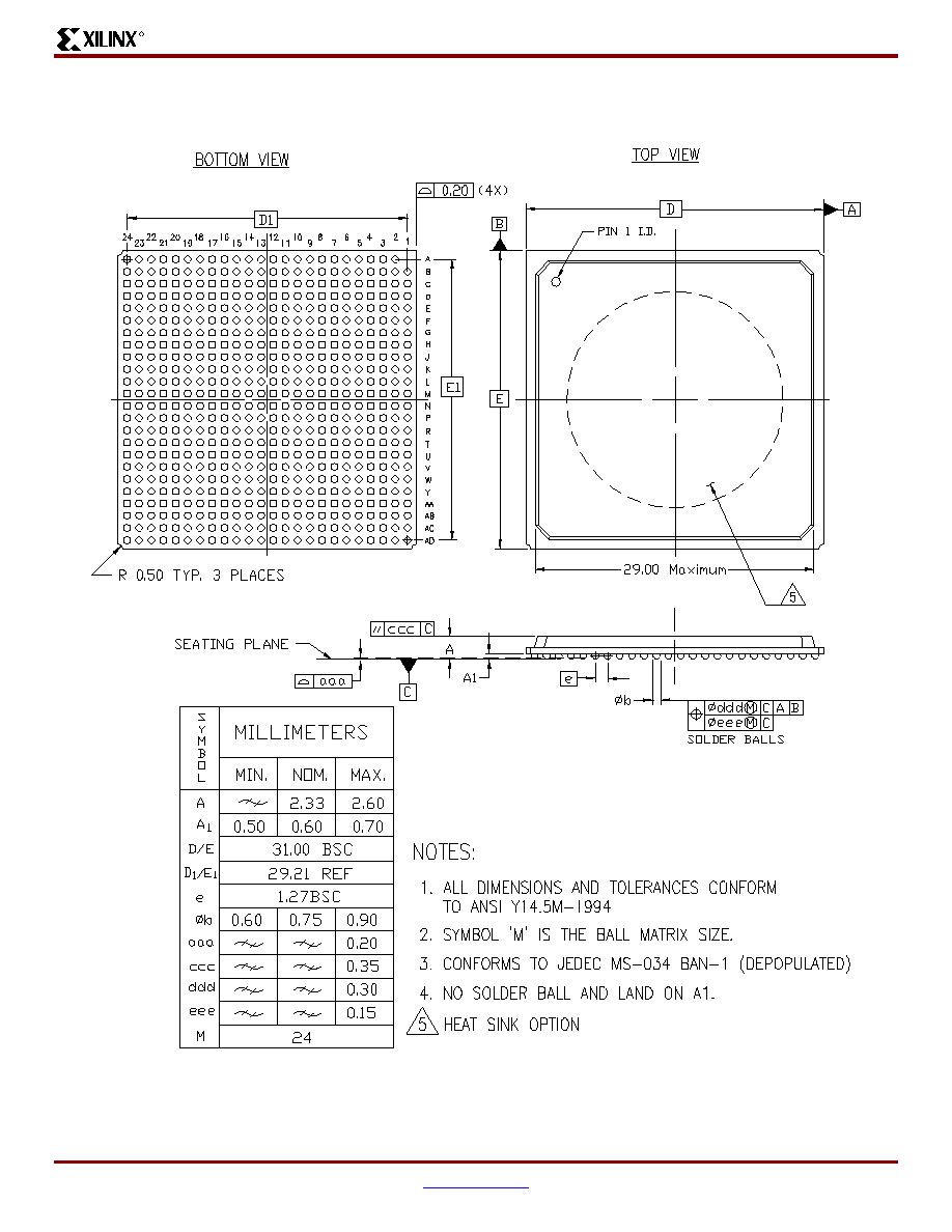
VirtexTM-II Platform FPGAs: Pinout Information
R
DS031-4 (v2.0) August 1, 2003
www.xilinx.com
Module 4 of 4
Product Specification
1-800-255-7778
71
BG575 Standard BGA Package Specifications (1.27mm pitch)
Figure 5: BG575 Standard BGA Package Specifications
VirtexTM-II Platform FPGAs: Pinout Information
R
DS031-4 (v2.0) August 1, 2003
www.xilinx.com
Module 4 of 4
Product Specification
1-800-255-7778
72
BG728 Standard BGA Package
As shown in
Table 10
, XC2V3000 Virtex-II devices are available in the BG728 BGA package. Following this table are the
BG728 Standard BGA Package Specifications (1.27mm pitch)
.
Table 10: BG728 BGA -- XC2V3000
Bank
Pin Description
Pin Number
0
IO_L01N_0
B3
0
IO_L01P_0
A3
0
IO_L02N_0
B4
0
IO_L02P_0
A4
0
IO_L03N_0/VRP_0
C5
0
IO_L03P_0/VRN_0
C6
0
IO_L04N_0/VREF_0
B5
0
IO_L04P_0
A5
0
IO_L05N_0
E6
0
IO_L05P_0
D6
0
IO_L06N_0
B6
0
IO_L06P_0
A6
0
IO_L19N_0
E7
0
IO_L19P_0
D8
0
IO_L21N_0
F8
0
IO_L21P_0/VREF_0
E8
0
IO_L22N_0
C7
0
IO_L22P_0
C8
0
IO_L24N_0
B7
0
IO_L24P_0
A7
0
IO_L25N_0
H9
0
IO_L25P_0
J9
0
IO_L27N_0
F9
0
IO_L27P_0/VREF_0
G9
0
IO_L28N_0
E9
0
IO_L28P_0
D9
0
IO_L30N_0
C9
0
IO_L30P_0
B9
0
IO_L49N_0
A8
0
IO_L49P_0
A9
0
IO_L51N_0
G10
0
IO_L51P_0/VREF_0
H10
0
IO_L52N_0
F10
VirtexTM-II Platform FPGAs: Pinout Information
R
DS031-4 (v2.0) August 1, 2003
www.xilinx.com
Module 4 of 4
Product Specification
1-800-255-7778
73
0
IO_L52P_0
E10
0
IO_L54N_0
D10
0
IO_L54P_0
C10
0
IO_L67N_0
B10
0
IO_L67P_0
A10
0
IO_L69N_0
G11
0
IO_L69P_0/VREF_0
H11
0
IO_L70N_0
F11
0
IO_L70P_0
F12
0
IO_L72N_0
D11
0
IO_L72P_0
C11
0
IO_L73N_0
B11
0
IO_L73P_0
A11
0
IO_L75N_0
H12
0
IO_L75P_0/VREF_0
J12
0
IO_L76N_0
E12
0
IO_L76P_0
D12
0
IO_L78N_0
B12
0
IO_L78P_0
A12
0
IO_L91N_0/VREF_0
J13
0
IO_L91P_0
H13
0
IO_L92N_0
G13
0
IO_L92P_0
F13
0
IO_L93N_0
E13
0
IO_L93P_0
D13
0
IO_L94N_0/VREF_0
B13
0
IO_L94P_0
A13
0
IO_L95N_0/GCLK7P
C13
0
IO_L95P_0/GCLK6S
C14
0
IO_L96N_0/GCLK5P
F14
0
IO_L96P_0/GCLK4S
E14
1
IO_L96N_1/GCLK3P
G14
1
IO_L96P_1/GCLK2S
H14
1
IO_L95N_1/GCLK1P
A15
1
IO_L95P_1/GCLK0S
B15
Table 10: BG728 BGA -- XC2V3000
Bank
Pin Description
Pin Number

VirtexTM-II Platform FPGAs: Pinout Information
R
DS031-4 (v2.0) August 1, 2003
www.xilinx.com
Module 4 of 4
Product Specification
1-800-255-7778
74
1
IO_L94N_1
C15
1
IO_L94P_1/VREF_1
D15
1
IO_L93N_1
E15
1
IO_L93P_1
F15
1
IO_L92N_1
G15
1
IO_L92P_1
H15
1
IO_L91N_1
J15
1
IO_L91P_1/VREF_1
J16
1
IO_L78N_1
A16
1
IO_L78P_1
B16
1
IO_L76N_1
D16
1
IO_L76P_1
E16
1
IO_L75N_1/VREF_1
F16
1
IO_L75P_1
F17
1
IO_L73N_1
H16
1
IO_L73P_1
H17
1
IO_L72N_1
A17
1
IO_L72P_1
B17
1
IO_L70N_1
C17
1
IO_L70P_1
D17
1
IO_L69N_1/VREF_1
G18
1
IO_L69P_1
G17
1
IO_L67N_1
A18
1
IO_L67P_1
B18
1
IO_L54N_1
C18
1
IO_L54P_1
D18
1
IO_L52N_1
E18
1
IO_L52P_1
F18
1
IO_L51N_1/VREF_1
H19
1
IO_L51P_1
H18
1
IO_L49N_1
A19
1
IO_L49P_1
A20
1
IO_L30N_1
B19
1
IO_L30P_1
C19
1
IO_L28N_1
D19
1
IO_L28P_1
E19
Table 10: BG728 BGA -- XC2V3000
Bank
Pin Description
Pin Number
VirtexTM-II Platform FPGAs: Pinout Information
R
DS031-4 (v2.0) August 1, 2003
www.xilinx.com
Module 4 of 4
Product Specification
1-800-255-7778
75
1
IO_L27N_1/VREF_1
F19
1
IO_L27P_1
G19
1
IO_L25N_1
J19
1
IO_L25P_1
J20
1
IO_L24N_1
C20
1
IO_L24P_1
C21
1
IO_L22N_1
D20
1
IO_L22P_1
E21
1
IO_L21N_1/VREF_1
E20
1
IO_L21P_1
F20
1
IO_L19N_1
A21
1
IO_L19P_1
B21
1
IO_L06N_1
A22
1
IO_L06P_1
B22
1
IO_L05N_1
C22
1
IO_L05P_1
C23
1
IO_L04N_1
D22
1
IO_L04P_1/VREF_1
E22
1
IO_L03N_1/VRP_1
A23
1
IO_L03P_1/VRN_1
B23
1
IO_L02N_1
A24
1
IO_L02P_1
B24
1
IO_L01N_1
A25
1
IO_L01P_1
B25
2
IO_L01N_2
C27
2
IO_L01P_2
D27
2
IO_L02N_2/VRP_2
D25
2
IO_L02P_2/VRN_2
D26
2
IO_L03N_2
E24
2
IO_L03P_2/VREF_2
E25
2
IO_L04N_2
E26
2
IO_L04P_2
E27
2
IO_L06N_2
F23
2
IO_L06P_2
F24
2
IO_L19N_2
F25
Table 10: BG728 BGA -- XC2V3000
Bank
Pin Description
Pin Number

VirtexTM-II Platform FPGAs: Pinout Information
R
DS031-4 (v2.0) August 1, 2003
www.xilinx.com
Module 4 of 4
Product Specification
1-800-255-7778
76
2
IO_L19P_2
F26
2
IO_L21N_2
F27
2
IO_L21P_2/VREF_2
G27
2
IO_L22N_2
G23
2
IO_L22P_2
H23
2
IO_L24N_2
G25
2
IO_L24P_2
G26
2
IO_L25N_2
H21
2
IO_L25P_2
J21
2
IO_L27N_2
H22
2
IO_L27P_2/VREF_2
J22
2
IO_L28N_2
H24
2
IO_L28P_2
H25
2
IO_L30N_2
H27
2
IO_L30P_2
J27
2
IO_L43N_2
J23
2
IO_L43P_2
J24
2
IO_L45N_2
J25
2
IO_L45P_2/VREF_2
J26
2
IO_L46N_2
K20
2
IO_L46P_2
K21
2
IO_L48N_2
K22
2
IO_L48P_2
K23
2
IO_L49N_2
K24
2
IO_L49P_2
K25
2
IO_L51N_2
K26
2
IO_L51P_2/VREF_2
K27
2
IO_L52N_2
L20
2
IO_L52P_2
M20
2
IO_L54N_2
L21
2
IO_L54P_2
L22
2
IO_L67N_2
L24
2
IO_L67P_2
L25
2
IO_L69N_2
L26
2
IO_L69P_2/VREF_2
L27
2
IO_L70N_2
M19
Table 10: BG728 BGA -- XC2V3000
Bank
Pin Description
Pin Number
VirtexTM-II Platform FPGAs: Pinout Information
R
DS031-4 (v2.0) August 1, 2003
www.xilinx.com
Module 4 of 4
Product Specification
1-800-255-7778
77
2
IO_L70P_2
N19
2
IO_L72N_2
M22
2
IO_L72P_2
M23
2
IO_L73N_2
M24
2
IO_L73P_2
N24
2
IO_L75N_2
M26
2
IO_L75P_2/VREF_2
M27
2
IO_L76N_2
N20
2
IO_L76P_2
N21
2
IO_L78N_2
N22
2
IO_L78P_2
N23
2
IO_L91N_2
N25
2
IO_L91P_2
P25
2
IO_L93N_2
N26
2
IO_L93P_2/VREF_2
N27
2
IO_L94N_2
P20
2
IO_L94P_2
P21
2
IO_L96N_2
P22
2
IO_L96P_2
P23
3
IO_L96N_3
R27
3
IO_L96P_3
R26
3
IO_L94N_3
R25
3
IO_L94P_3
R24
3
IO_L93N_3/VREF_3
R23
3
IO_L93P_3
T23
3
IO_L91N_3
R22
3
IO_L91P_3
R21
3
IO_L78N_3
R20
3
IO_L78P_3
R19
3
IO_L76N_3
T27
3
IO_L76P_3
T26
3
IO_L75N_3/VREF_3
T24
3
IO_L75P_3
U24
3
IO_L73N_3
T22
3
IO_L73P_3
U22
Table 10: BG728 BGA -- XC2V3000
Bank
Pin Description
Pin Number

VirtexTM-II Platform FPGAs: Pinout Information
R
DS031-4 (v2.0) August 1, 2003
www.xilinx.com
Module 4 of 4
Product Specification
1-800-255-7778
78
3
IO_L72N_3
T20
3
IO_L72P_3
T19
3
IO_L70N_3
U27
3
IO_L70P_3
U26
3
IO_L69N_3/VREF_3
U25
3
IO_L69P_3
V25
3
IO_L67N_3
U21
3
IO_L67P_3
U20
3
IO_L54N_3
V27
3
IO_L54P_3
V26
3
IO_L52N_3
V24
3
IO_L52P_3
V23
3
IO_L51N_3/VREF_3
V22
3
IO_L51P_3
W22
3
IO_L49N_3
V21
3
IO_L49P_3
V20
3
IO_L48N_3
W27
3
IO_L48P_3
Y27
3
IO_L46N_3
W26
3
IO_L46P_3
W25
3
IO_L45N_3/VREF_3
W24
3
IO_L45P_3
W23
3
IO_L43N_3
W21
3
IO_L43P_3
W20
3
IO_L28N_3
W19
3
IO_L28P_3
Y19
3
IO_L27N_3/VREF_3
Y25
3
IO_L27P_3
Y24
3
IO_L25N_3
Y23
3
IO_L25P_3
AA23
3
IO_L24N_3
Y22
3
IO_L24P_3
Y21
3
IO_L22N_3
AA27
3
IO_L22P_3
AB27
3
IO_L21N_3/VREF_3
AA26
3
IO_L21P_3
AA25
Table 10: BG728 BGA -- XC2V3000
Bank
Pin Description
Pin Number

VirtexTM-II Platform FPGAs: Pinout Information
R
DS031-4 (v2.0) August 1, 2003
www.xilinx.com
Module 4 of 4
Product Specification
1-800-255-7778
79
3
IO_L19N_3
AB26
3
IO_L19P_3
AB25
3
IO_L06N_3
AB24
3
IO_L06P_3
AB23
3
IO_L04N_3
AC27
3
IO_L04P_3
AC26
3
IO_L03N_3/VREF_3
AC25
3
IO_L03P_3
AC24
3
IO_L02N_3/VRP_3
AD27
3
IO_L02P_3/VRN_3
AE27
3
IO_L01N_3
AD26
3
IO_L01P_3
AD25
4
IO_L01N_4/BUSY/DOUT
(1)
AF25
4
IO_L01P_4/INIT_B
AG25
4
IO_L02N_4/D0/DIN
(1)
AF24
4
IO_L02P_4/D1
AG24
4
IO_L03N_4/D2/ALT_VRP_4
AD23
4
IO_L03P_4/D3/ALT_VRN_4
AE23
4
IO_L04N_4/VREF_4
AF23
4
IO_L04P_4
AG23
4
IO_L05N_4/VRP_4
AD22
4
IO_L05P_4/VRN_4
AE22
4
IO_L06N_4
AF22
4
IO_L06P_4
AG22
4
IO_L19N_4
AC21
4
IO_L19P_4
AB21
4
IO_L21N_4
AE21
4
IO_L21P_4/VREF_4
AE20
4
IO_L22N_4
AF21
4
IO_L22P_4
AG21
4
IO_L24N_4
AB20
4
IO_L24P_4
AA20
4
IO_L25N_4
AC20
4
IO_L25P_4
AD20
4
IO_L27N_4
AG20
Table 10: BG728 BGA -- XC2V3000
Bank
Pin Description
Pin Number

VirtexTM-II Platform FPGAs: Pinout Information
R
DS031-4 (v2.0) August 1, 2003
www.xilinx.com
Module 4 of 4
Product Specification
1-800-255-7778
80
4
IO_L27P_4/VREF_4
AG19
4
IO_L28N_4
AB19
4
IO_L28P_4
AA19
4
IO_L30N_4
AC19
4
IO_L30P_4
AD19
4
IO_L49N_4
AE19
4
IO_L49P_4
AF19
4
IO_L51N_4
AA18
4
IO_L51P_4/VREF_4
Y18
4
IO_L52N_4
AB18
4
IO_L52P_4
AC18
4
IO_L54N_4
AD18
4
IO_L54P_4
AE18
4
IO_L67N_4
AF18
4
IO_L67P_4
AG18
4
IO_L69N_4
AA17
4
IO_L69P_4/VREF_4
Y17
4
IO_L70N_4
AB17
4
IO_L70P_4
AB16
4
IO_L72N_4
AD17
4
IO_L72P_4
AE17
4
IO_L73N_4
AF17
4
IO_L73P_4
AG17
4
IO_L75N_4
Y16
4
IO_L75P_4/VREF_4
W16
4
IO_L76N_4
AC16
4
IO_L76P_4
AD16
4
IO_L78N_4
AF16
4
IO_L78P_4
AG16
4
IO_L91N_4/VREF_4
W15
4
IO_L91P_4
Y15
4
IO_L92N_4
AB15
4
IO_L92P_4
AA15
4
IO_L93N_4
AC15
4
IO_L93P_4
AD15
4
IO_L94N_4/VREF_4
AE15
Table 10: BG728 BGA -- XC2V3000
Bank
Pin Description
Pin Number
VirtexTM-II Platform FPGAs: Pinout Information
R
DS031-4 (v2.0) August 1, 2003
www.xilinx.com
Module 4 of 4
Product Specification
1-800-255-7778
81
4
IO_L94P_4
AE14
4
IO_L95N_4/GCLK3S
AF15
4
IO_L95P_4/GCLK2P
AG15
4
IO_L96N_4/GCLK1S
Y14
4
IO_L96P_4/GCLK0P
AA14
5
IO_L96N_5/GCLK7S
AC14
5
IO_L96P_5/GCLK6P
AB14
5
IO_L95N_5/GCLK5S
AG13
5
IO_L95P_5/GCLK4P
AF13
5
IO_L94N_5
AE13
5
IO_L94P_5/VREF_5
AD13
5
IO_L93N_5
AC13
5
IO_L93P_5
AB13
5
IO_L92N_5
AA13
5
IO_L92P_5
Y13
5
IO_L91N_5
W13
5
IO_L91P_5/VREF_5
W12
5
IO_L78N_5
AG12
5
IO_L78P_5
AF12
5
IO_L76N_5
AD12
5
IO_L76P_5
AC12
5
IO_L75N_5/VREF_5
AB12
5
IO_L75P_5
AB11
5
IO_L73N_5
Y12
5
IO_L73P_5
Y11
5
IO_L72N_5
AG11
5
IO_L72P_5
AF11
5
IO_L70N_5
AE11
5
IO_L70P_5
AD11
5
IO_L69N_5/VREF_5
AA10
5
IO_L69P_5
AA11
5
IO_L67N_5
AG10
5
IO_L67P_5
AF10
5
IO_L54N_5
AE10
5
IO_L54P_5
AD10
Table 10: BG728 BGA -- XC2V3000
Bank
Pin Description
Pin Number

VirtexTM-II Platform FPGAs: Pinout Information
R
DS031-4 (v2.0) August 1, 2003
www.xilinx.com
Module 4 of 4
Product Specification
1-800-255-7778
82
5
IO_L52N_5
AC10
5
IO_L52P_5
AB10
5
IO_L51N_5/VREF_5
Y9
5
IO_L51P_5
Y10
5
IO_L49N_5
AG9
5
IO_L49P_5
AG8
5
IO_L30N_5
AF9
5
IO_L30P_5
AE9
5
IO_L28N_5
AD9
5
IO_L28P_5
AC9
5
IO_L27N_5/VREF_5
AB9
5
IO_L27P_5
AA9
5
IO_L25N_5
AE8
5
IO_L25P_5
AE7
5
IO_L24N_5
AD8
5
IO_L24P_5
AC8
5
IO_L22N_5
AB8
5
IO_L22P_5
AA8
5
IO_L21N_5/VREF_5
AG7
5
IO_L21P_5
AF7
5
IO_L19N_5
AC7
5
IO_L19P_5
AB7
5
IO_L06N_5
AG6
5
IO_L06P_5
AF6
5
IO_L05N_5/VRP_5
AE6
5
IO_L05P_5/VRN_5
AD6
5
IO_L04N_5
AG5
5
IO_L04P_5/VREF_5
AF5
5
IO_L03N_5/D4/ALT_VRP_5
AE5
5
IO_L03P_5/D5/ALT_VRN_5
AD5
5
IO_L02N_5/D6
AG4
5
IO_L02P_5/D7
AF4
5
IO_L01N_5/RDWR_B
AG3
5
IO_L01P_5/CS_B
AF3
6
IO_L01P_6
AE1
Table 10: BG728 BGA -- XC2V3000
Bank
Pin Description
Pin Number

VirtexTM-II Platform FPGAs: Pinout Information
R
DS031-4 (v2.0) August 1, 2003
www.xilinx.com
Module 4 of 4
Product Specification
1-800-255-7778
83
6
IO_L01N_6
AD1
6
IO_L02P_6/VRN_6
AD3
6
IO_L02N_6/VRP_6
AD2
6
IO_L03P_6
AC4
6
IO_L03N_6/VREF_6
AC3
6
IO_L04P_6
AC2
6
IO_L04N_6
AC1
6
IO_L06P_6
AB5
6
IO_L06N_6
AB4
6
IO_L19P_6
AB3
6
IO_L19N_6
AB2
6
IO_L21P_6
AB1
6
IO_L21N_6/VREF_6
AA1
6
IO_L22P_6
AA5
6
IO_L22N_6
AA6
6
IO_L24P_6
AA3
6
IO_L24N_6
AA2
6
IO_L25P_6
Y5
6
IO_L25N_6
Y6
6
IO_L27P_6
Y4
6
IO_L27N_6/VREF_6
Y3
6
IO_L28P_6
Y1
6
IO_L28N_6
W1
6
IO_L43P_6
W8
6
IO_L43N_6
W9
6
IO_L45P_6
W6
6
IO_L45N_6/VREF_6
W7
6
IO_L46P_6
W5
6
IO_L46N_6
W4
6
IO_L48P_6
W3
6
IO_L48N_6
W2
6
IO_L49P_6
V7
6
IO_L49N_6
V8
6
IO_L51P_6
V5
6
IO_L51N_6/VREF_6
V6
6
IO_L52P_6
V4
Table 10: BG728 BGA -- XC2V3000
Bank
Pin Description
Pin Number
VirtexTM-II Platform FPGAs: Pinout Information
R
DS031-4 (v2.0) August 1, 2003
www.xilinx.com
Module 4 of 4
Product Specification
1-800-255-7778
84
6
IO_L52N_6
V3
6
IO_L54P_6
V2
6
IO_L54N_6
V1
6
IO_L67P_6
U8
6
IO_L67N_6
T8
6
IO_L69P_6
U6
6
IO_L69N_6/VREF_6
U7
6
IO_L70P_6
U4
6
IO_L70N_6
U3
6
IO_L72P_6
U2
6
IO_L72N_6
U1
6
IO_L73P_6
T9
6
IO_L73N_6
R9
6
IO_L75P_6
T5
6
IO_L75N_6/VREF_6
T6
6
IO_L76P_6
T4
6
IO_L76N_6
R4
6
IO_L78P_6
T2
6
IO_L78N_6
T1
6
IO_L91P_6
R7
6
IO_L91N_6
R8
6
IO_L93P_6
R5
6
IO_L93N_6/VREF_6
R6
6
IO_L94P_6
R3
6
IO_L94N_6
P3
6
IO_L96P_6
R2
6
IO_L96N_6
R1
7
IO_L96P_7
P5
7
IO_L96N_7
P6
7
IO_L94P_7
P7
7
IO_L94N_7
P8
7
IO_L93P_7/VREF_7
N1
7
IO_L93N_7
N2
7
IO_L91P_7
N3
7
IO_L91N_7
N4
Table 10: BG728 BGA -- XC2V3000
Bank
Pin Description
Pin Number
VirtexTM-II Platform FPGAs: Pinout Information
R
DS031-4 (v2.0) August 1, 2003
www.xilinx.com
Module 4 of 4
Product Specification
1-800-255-7778
85
7
IO_L78P_7
N6
7
IO_L78N_7
N7
7
IO_L76P_7
N9
7
IO_L76N_7
N8
7
IO_L75P_7/VREF_7
N5
7
IO_L75N_7
M6
7
IO_L73P_7
M1
7
IO_L73N_7
M2
7
IO_L72P_7
M4
7
IO_L72N_7
M5
7
IO_L70P_7
M8
7
IO_L70N_7
M9
7
IO_L69P_7/VREF_7
L1
7
IO_L69N_7
L2
7
IO_L67P_7
L3
7
IO_L67N_7
L4
7
IO_L54P_7
K1
7
IO_L54N_7
K2
7
IO_L52P_7
K4
7
IO_L52N_7
K5
7
IO_L51P_7/VREF_7
L6
7
IO_L51N_7
L7
7
IO_L49P_7
K6
7
IO_L49N_7
K7
7
IO_L48P_7
L8
7
IO_L48N_7
K8
7
IO_L46P_7
J1
7
IO_L46N_7
H1
7
IO_L45P_7/VREF_7
J2
7
IO_L45N_7
J3
7
IO_L43P_7
K3
7
IO_L43N_7
J4
7
IO_L30P_7
H3
7
IO_L30N_7
H4
7
IO_L28P_7
J5
7
IO_L28N_7
J6
Table 10: BG728 BGA -- XC2V3000
Bank
Pin Description
Pin Number
VirtexTM-II Platform FPGAs: Pinout Information
R
DS031-4 (v2.0) August 1, 2003
www.xilinx.com
Module 4 of 4
Product Specification
1-800-255-7778
86
7
IO_L27P_7/VREF_7
H5
7
IO_L27N_7
H6
7
IO_L25P_7
J7
7
IO_L25N_7
J8
7
IO_L24P_7
G1
7
IO_L24N_7
F1
7
IO_L22P_7
G2
7
IO_L22N_7
G3
7
IO_L21P_7/VREF_7
F2
7
IO_L21N_7
F3
7
IO_L19P_7
G5
7
IO_L19N_7
G6
7
IO_L06P_7
F4
7
IO_L06N_7
F5
7
IO_L04P_7
E1
7
IO_L04N_7
E2
7
IO_L03P_7/VREF_7
D1
7
IO_L03N_7
C1
7
IO_L02P_7/VRN_7
E3
7
IO_L02N_7/VRP_7
E4
7
IO_L01P_7
D2
7
IO_L01N_7
D3
0
VCCO_0
K13
0
VCCO_0
K12
0
VCCO_0
K11
0
VCCO_0
J11
0
VCCO_0
J10
0
VCCO_0
G12
0
VCCO_0
D7
0
VCCO_0
C12
1
VCCO_1
K17
1
VCCO_1
K16
1
VCCO_1
K15
1
VCCO_1
J18
1
VCCO_1
J17
Table 10: BG728 BGA -- XC2V3000
Bank
Pin Description
Pin Number

VirtexTM-II Platform FPGAs: Pinout Information
R
DS031-4 (v2.0) August 1, 2003
www.xilinx.com
Module 4 of 4
Product Specification
1-800-255-7778
87
1
VCCO_1
G16
1
VCCO_1
D21
1
VCCO_1
C16
2
VCCO_2
N18
2
VCCO_2
M25
2
VCCO_2
M21
2
VCCO_2
M18
2
VCCO_2
L19
2
VCCO_2
L18
2
VCCO_2
K19
2
VCCO_2
G24
3
VCCO_3
AA24
3
VCCO_3
V19
3
VCCO_3
U19
3
VCCO_3
U18
3
VCCO_3
T25
3
VCCO_3
T21
3
VCCO_3
T18
3
VCCO_3
R18
4
VCCO_4
AE16
4
VCCO_4
AD21
4
VCCO_4
AA16
4
VCCO_4
W18
4
VCCO_4
W17
4
VCCO_4
V17
4
VCCO_4
V16
4
VCCO_4
V15
5
VCCO_5
AE12
5
VCCO_5
AD7
5
VCCO_5
AA12
5
VCCO_5
W11
5
VCCO_5
W10
5
VCCO_5
V13
5
VCCO_5
V12
5
VCCO_5
V11
6
VCCO_6
AA4
Table 10: BG728 BGA -- XC2V3000
Bank
Pin Description
Pin Number
VirtexTM-II Platform FPGAs: Pinout Information
R
DS031-4 (v2.0) August 1, 2003
www.xilinx.com
Module 4 of 4
Product Specification
1-800-255-7778
88
6
VCCO_6
V9
6
VCCO_6
U10
6
VCCO_6
U9
6
VCCO_6
T10
6
VCCO_6
T7
6
VCCO_6
T3
6
VCCO_6
R10
7
VCCO_7
M10
7
VCCO_7
M7
7
VCCO_7
M3
7
VCCO_7
L10
7
VCCO_7
L9
7
VCCO_7
K9
7
VCCO_7
G4
7
VCCO_7
N10
NA
CCLK
AA22
NA
PROG_B
C4
NA
DONE
AC22
NA
M0
AC6
NA
M1
Y7
NA
M2
AE4
NA
HSWAP_EN
D5
NA
TCK
G20
NA
TDI
H7
NA
TDO
G22
NA
TMS
F21
NA
PWRDWN_B
AE24
NA
DXN
G8
NA
DXP
F7
NA
VBATT
D23
NA
RSVD
C24
NA
VCCAUX
AF14
NA
VCCAUX
AE26
NA
VCCAUX
AE2
Table 10: BG728 BGA -- XC2V3000
Bank
Pin Description
Pin Number

VirtexTM-II Platform FPGAs: Pinout Information
R
DS031-4 (v2.0) August 1, 2003
www.xilinx.com
Module 4 of 4
Product Specification
1-800-255-7778
89
NA
VCCAUX
P26
NA
VCCAUX
P2
NA
VCCAUX
C26
NA
VCCAUX
C2
NA
VCCAUX
B14
NA
VCCINT
V18
NA
VCCINT
V14
NA
VCCINT
V10
NA
VCCINT
U17
NA
VCCINT
U16
NA
VCCINT
U15
NA
VCCINT
U14
NA
VCCINT
U13
NA
VCCINT
U12
NA
VCCINT
U11
NA
VCCINT
T17
NA
VCCINT
T11
NA
VCCINT
R17
NA
VCCINT
R11
NA
VCCINT
P18
NA
VCCINT
P17
NA
VCCINT
P11
NA
VCCINT
P10
NA
VCCINT
N17
NA
VCCINT
N11
NA
VCCINT
M17
NA
VCCINT
M11
NA
VCCINT
L17
NA
VCCINT
L16
NA
VCCINT
L15
NA
VCCINT
L14
NA
VCCINT
L13
NA
VCCINT
L12
NA
VCCINT
L11
NA
VCCINT
K18
NA
VCCINT
K14
Table 10: BG728 BGA -- XC2V3000
Bank
Pin Description
Pin Number

VirtexTM-II Platform FPGAs: Pinout Information
R
DS031-4 (v2.0) August 1, 2003
www.xilinx.com
Module 4 of 4
Product Specification
1-800-255-7778
90
NA
VCCINT
K10
NA
GND
AG27
NA
GND
AG26
NA
GND
AG14
NA
GND
AG2
NA
GND
AG1
NA
GND
AF27
NA
GND
AF26
NA
GND
AF20
NA
GND
AF8
NA
GND
AF2
NA
GND
AF1
NA
GND
AE25
NA
GND
AE3
NA
GND
AD24
NA
GND
AD14
NA
GND
AD4
NA
GND
AC23
NA
GND
AC17
NA
GND
AC11
NA
GND
AC5
NA
GND
AB22
NA
GND
AB6
NA
GND
AA21
NA
GND
AA7
NA
GND
Y26
NA
GND
Y20
NA
GND
Y8
NA
GND
Y2
NA
GND
W14
NA
GND
U23
NA
GND
U5
NA
GND
T16
NA
GND
T15
NA
GND
T14
NA
GND
T13
Table 10: BG728 BGA -- XC2V3000
Bank
Pin Description
Pin Number

VirtexTM-II Platform FPGAs: Pinout Information
R
DS031-4 (v2.0) August 1, 2003
www.xilinx.com
Module 4 of 4
Product Specification
1-800-255-7778
91
NA
GND
T12
NA
GND
R16
NA
GND
R15
NA
GND
R14
NA
GND
R13
NA
GND
R12
NA
GND
P27
NA
GND
P24
NA
GND
P19
NA
GND
P16
NA
GND
P15
NA
GND
P14
NA
GND
P13
NA
GND
P12
NA
GND
P9
NA
GND
P4
NA
GND
P1
NA
GND
N16
NA
GND
N15
NA
GND
N14
NA
GND
N13
NA
GND
N12
NA
GND
M16
NA
GND
M15
NA
GND
M14
NA
GND
M13
NA
GND
M12
NA
GND
L23
NA
GND
L5
NA
GND
J14
NA
GND
H26
NA
GND
H20
NA
GND
H8
NA
GND
H2
NA
GND
G21
NA
GND
G7
Table 10: BG728 BGA -- XC2V3000
Bank
Pin Description
Pin Number

VirtexTM-II Platform FPGAs: Pinout Information
R
DS031-4 (v2.0) August 1, 2003
www.xilinx.com
Module 4 of 4
Product Specification
1-800-255-7778
92
NA
GND
F22
NA
GND
F6
NA
GND
E23
NA
GND
E17
NA
GND
E11
NA
GND
E5
NA
GND
D24
NA
GND
D14
NA
GND
D4
NA
GND
C25
NA
GND
C3
NA
GND
B27
NA
GND
B26
NA
GND
B20
NA
GND
B8
NA
GND
B2
NA
GND
B1
NA
GND
A27
NA
GND
A26
NA
GND
A14
NA
GND
A2
Notes:
1.
See
Table 4
for an explanation of the signals available on this pin.
Table 10: BG728 BGA -- XC2V3000
Bank
Pin Description
Pin Number
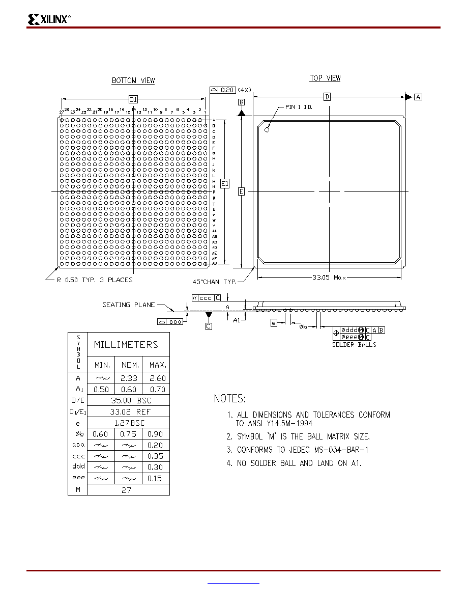
VirtexTM-II Platform FPGAs: Pinout Information
R
DS031-4 (v2.0) August 1, 2003
www.xilinx.com
Module 4 of 4
Product Specification
1-800-255-7778
93
BG728 Standard BGA Package Specifications (1.27mm pitch)
Figure 6: BG728 Standard BGA Package Specifications
VirtexTM-II Platform FPGAs: Pinout Information
R
DS031-4 (v2.0) August 1, 2003
www.xilinx.com
Module 4 of 4
Product Specification
1-800-255-7778
94
FF896 Flip-Chip Fine-Pitch BGA Package
As shown in
Table 11
, XC2V1000, XC2V1500, and XC2V2000 Virtex-II devices are available in the FF896 flip-chip fine-pitch
BGA package. Pins in the XC2V1000, XC2V1500, and XC2V2000 devices are the same, except for the pin differences in the
XC2V1000 and XC2V1500 devices shown in the No Connect columns. Following this table are the
FF896 Flip-Chip
Fine-Pitch BGA Package Specifications (1.00mm pitch)
.
Table 11: FF896 BGA -- XC2V1000, XC2V1500, and XC2V2000
Bank
Pin Description
Pin Number
No Connect in the XC2V1000
No Connect in the XC2V1500
0
IO_L01N_0
B27
0
IO_L01P_0
A27
0
IO_L02N_0
F24
0
IO_L02P_0
E24
0
IO_L03N_0/VRP_0
C26
0
IO_L03P_0/VRN_0
C25
0
IO_L04N_0/VREF_0
A26
0
IO_L04P_0
A25
0
IO_L05N_0
F23
0
IO_L05P_0
F22
0
IO_L06N_0
C24
0
IO_L06P_0
D25
0
IO_L19N_0
A24
0
IO_L19P_0
B25
0
IO_L20N_0
G22
0
IO_L20P_0
G21
0
IO_L21N_0
D24
0
IO_L21P_0/VREF_0
D23
0
IO_L22N_0
B23
0
IO_L22P_0
B24
0
IO_L23N_0
H21
0
IO_L23P_0
H20
0
IO_L24N_0
E22
0
IO_L24P_0
E23
0
IO_L49N_0
A22
0
IO_L49P_0
B22
0
IO_L50N_0
F21
0
IO_L50P_0
F20
0
IO_L51N_0
C23
0
IO_L51P_0/VREF_0
C22
0
IO_L52N_0
B20
0
IO_L52P_0
B21

VirtexTM-II Platform FPGAs: Pinout Information
R
DS031-4 (v2.0) August 1, 2003
www.xilinx.com
Module 4 of 4
Product Specification
1-800-255-7778
95
0
IO_L53N_0
G20
0
IO_L53P_0
G19
0
IO_L54N_0
D21
0
IO_L54P_0
D22
0
IO_L67N_0
E20
NC
0
IO_L67P_0
E21
NC
0
IO_L68N_0
H19
NC
0
IO_L68P_0
H18
NC
0
IO_L69N_0
D20
NC
0
IO_L69P_0/VREF_0
D19
NC
0
IO_L70N_0
A20
NC
0
IO_L70P_0
A21
NC
0
IO_L71N_0
F19
NC
0
IO_L71P_0
F18
NC
0
IO_L72N_0
C19
NC
0
IO_L72P_0
C20
NC
0
IO_L73N_0
B18
NC
NC
0
IO_L73P_0
B19
NC
NC
0
IO_L74N_0
G18
NC
NC
0
IO_L74P_0
H17
NC
NC
0
IO_L75N_0
E18
NC
NC
0
IO_L75P_0/VREF_0
D18
NC
NC
0
IO_L76N_0
A18
NC
NC
0
IO_L76P_0
A19
NC
NC
0
IO_L77N_0
J17
NC
NC
0
IO_L77P_0
J16
NC
NC
0
IO_L78N_0
E16
NC
NC
0
IO_L78P_0
E17
NC
NC
0
IO_L91N_0/VREF_0
B17
0
IO_L91P_0
B16
0
IO_L92N_0
F17
0
IO_L92P_0
F16
0
IO_L93N_0
D16
0
IO_L93P_0
D17
0
IO_L94N_0/VREF_0
A17
0
IO_L94P_0
A16
0
IO_L95N_0/GCLK7P
H16
Table 11: FF896 BGA -- XC2V1000, XC2V1500, and XC2V2000
Bank
Pin Description
Pin Number
No Connect in the XC2V1000
No Connect in the XC2V1500

VirtexTM-II Platform FPGAs: Pinout Information
R
DS031-4 (v2.0) August 1, 2003
www.xilinx.com
Module 4 of 4
Product Specification
1-800-255-7778
96
0
IO_L95P_0/GCLK6S
G16
0
IO_L96N_0/GCLK5P
C17
0
IO_L96P_0/GCLK4S
C16
1
IO_L96N_1/GCLK3P
C15
1
IO_L96P_1/GCLK2S
C14
1
IO_L95N_1/GCLK1P
F15
1
IO_L95P_1/GCLK0S
F14
1
IO_L94N_1
B15
1
IO_L94P_1/VREF_1
B14
1
IO_L93N_1
D14
1
IO_L93P_1
D15
1
IO_L92N_1
G15
1
IO_L92P_1
H15
1
IO_L91N_1
A14
1
IO_L91P_1/VREF_1
A13
1
IO_L78N_1
E14
NC
NC
1
IO_L78P_1
E15
NC
NC
1
IO_L77N_1
J15
NC
NC
1
IO_L77P_1
J14
NC
NC
1
IO_L76N_1
B12
NC
NC
1
IO_L76P_1
B13
NC
NC
1
IO_L75N_1/VREF_1
D13
NC
NC
1
IO_L75P_1
E13
NC
NC
1
IO_L74N_1
H14
NC
NC
1
IO_L74P_1
H13
NC
NC
1
IO_L73N_1
A11
NC
NC
1
IO_L73P_1
A12
NC
NC
1
IO_L72N_1
C11
NC
1
IO_L72P_1
C12
NC
1
IO_L71N_1
F13
NC
1
IO_L71P_1
F12
NC
1
IO_L70N_1
B10
NC
1
IO_L70P_1
B11
NC
1
IO_L69N_1/VREF_1
D12
NC
1
IO_L69P_1
D11
NC
1
IO_L68N_1
G13
NC
Table 11: FF896 BGA -- XC2V1000, XC2V1500, and XC2V2000
Bank
Pin Description
Pin Number
No Connect in the XC2V1000
No Connect in the XC2V1500

VirtexTM-II Platform FPGAs: Pinout Information
R
DS031-4 (v2.0) August 1, 2003
www.xilinx.com
Module 4 of 4
Product Specification
1-800-255-7778
97
1
IO_L68P_1
G12
NC
1
IO_L67N_1
A9
NC
1
IO_L67P_1
A10
NC
1
IO_L54N_1
E10
1
IO_L54P_1
E11
1
IO_L53N_1
H12
1
IO_L53P_1
H11
1
IO_L52N_1
D9
1
IO_L52P_1
D10
1
IO_L51N_1/VREF_1
C9
1
IO_L51P_1
C8
1
IO_L50N_1
F11
1
IO_L50P_1
F10
1
IO_L49N_1
B8
1
IO_L49P_1
B9
1
IO_L24N_1
E8
1
IO_L24P_1
E9
1
IO_L23N_1
G11
1
IO_L23P_1
H10
1
IO_L22N_1
B7
1
IO_L22P_1
A7
1
IO_L21N_1/VREF_1
D8
1
IO_L21P_1
E7
1
IO_L20N_1
G10
1
IO_L20P_1
G9
1
IO_L19N_1
A5
1
IO_L19P_1
A6
1
IO_L06N_1
C6
1
IO_L06P_1
C7
1
IO_L05N_1
F9
1
IO_L05P_1
G8
1
IO_L04N_1
B6
1
IO_L04P_1/VREF_1
C5
1
IO_L03N_1/VRP_1
D7
1
IO_L03P_1/VRN_1
D6
1
IO_L02N_1
F8
1
IO_L02P_1
F7
Table 11: FF896 BGA -- XC2V1000, XC2V1500, and XC2V2000
Bank
Pin Description
Pin Number
No Connect in the XC2V1000
No Connect in the XC2V1500

VirtexTM-II Platform FPGAs: Pinout Information
R
DS031-4 (v2.0) August 1, 2003
www.xilinx.com
Module 4 of 4
Product Specification
1-800-255-7778
98
1
IO_L01N_1
B4
1
IO_L01P_1
A4
2
IO_L01N_2
C1
2
IO_L01P_2
B1
2
IO_L02N_2/VRP_2
H9
2
IO_L02P_2/VRN_2
H8
2
IO_L03N_2
D3
2
IO_L03P_2/VREF_2
E3
2
IO_L04N_2
D2
2
IO_L04P_2
C2
2
IO_L05N_2
G7
2
IO_L05P_2
H7
2
IO_L06N_2
F4
2
IO_L06P_2
E4
2
IO_L19N_2
E1
2
IO_L19P_2
D1
2
IO_L20N_2
G6
2
IO_L20P_2
H6
2
IO_L21N_2
F5
2
IO_L21P_2/VREF_2
G5
2
IO_L22N_2
G2
2
IO_L22P_2
F2
2
IO_L23N_2
J8
2
IO_L23P_2
J7
2
IO_L24N_2
G3
2
IO_L24P_2
F3
2
IO_L43N_2
G1
2
IO_L43P_2
F1
2
IO_L44N_2
K8
2
IO_L44P_2
L8
2
IO_L45N_2
G4
2
IO_L45P_2/VREF_2
H4
2
IO_L46N_2
J2
2
IO_L46P_2
H2
2
IO_L47N_2
J6
2
IO_L47P_2
K6
Table 11: FF896 BGA -- XC2V1000, XC2V1500, and XC2V2000
Bank
Pin Description
Pin Number
No Connect in the XC2V1000
No Connect in the XC2V1500

VirtexTM-II Platform FPGAs: Pinout Information
R
DS031-4 (v2.0) August 1, 2003
www.xilinx.com
Module 4 of 4
Product Specification
1-800-255-7778
99
2
IO_L48N_2
J5
2
IO_L48P_2
H5
2
IO_L49N_2
J3
2
IO_L49P_2
H3
2
IO_L50N_2
K7
2
IO_L50P_2
L7
2
IO_L51N_2
J4
2
IO_L51P_2/VREF_2
K4
2
IO_L52N_2
K1
2
IO_L52P_2
J1
2
IO_L53N_2
L6
2
IO_L53P_2
M6
2
IO_L54N_2
L5
2
IO_L54P_2
K5
2
IO_L67N_2
L2
NC
2
IO_L67P_2
K2
NC
2
IO_L68N_2
M8
NC
2
IO_L68P_2
N8
NC
2
IO_L69N_2
L4
NC
2
IO_L69P_2/VREF_2
M4
NC
2
IO_L70N_2
M1
NC
2
IO_L70P_2
L1
NC
2
IO_L71N_2
M7
NC
2
IO_L71P_2
N7
NC
2
IO_L72N_2
M3
NC
2
IO_L72P_2
L3
NC
2
IO_L73N_2
N2
NC
NC
2
IO_L73P_2
M2
NC
NC
2
IO_L74N_2
N6
NC
NC
2
IO_L74P_2
P6
NC
NC
2
IO_L75N_2
N5
NC
NC
2
IO_L75P_2/VREF_2
N4
NC
NC
2
IO_L76N_2
P1
NC
NC
2
IO_L76P_2
N1
NC
NC
2
IO_L77N_2
P9
NC
NC
2
IO_L77P_2
R9
NC
NC
2
IO_L78N_2
R5
NC
NC
Table 11: FF896 BGA -- XC2V1000, XC2V1500, and XC2V2000
Bank
Pin Description
Pin Number
No Connect in the XC2V1000
No Connect in the XC2V1500

VirtexTM-II Platform FPGAs: Pinout Information
R
DS031-4 (v2.0) August 1, 2003
www.xilinx.com
Module 4 of 4
Product Specification
1-800-255-7778
100
2
IO_L78P_2
P5
NC
NC
2
IO_L91N_2
R2
2
IO_L91P_2
P2
2
IO_L92N_2
P8
2
IO_L92P_2
R8
2
IO_L93N_2
P4
2
IO_L93P_2/VREF_2
R4
2
IO_L94N_2
R1
2
IO_L94P_2
T2
2
IO_L95N_2
R7
2
IO_L95P_2
R6
2
IO_L96N_2
R3
2
IO_L96P_2
P3
3
IO_L96N_3
T7
3
IO_L96P_3
T6
3
IO_L95N_3
U1
3
IO_L95P_3
V1
3
IO_L94N_3
T3
3
IO_L94P_3
U3
3
IO_L93N_3/VREF_3
T8
3
IO_L93P_3
U8
3
IO_L92N_3
U2
3
IO_L92P_3
V2
3
IO_L91N_3
T4
3
IO_L91P_3
U4
3
IO_L78N_3
U9
NC
NC
3
IO_L78P_3
T9
NC
NC
3
IO_L77N_3
W1
NC
NC
3
IO_L77P_3
Y1
NC
NC
3
IO_L76N_3
T5
NC
NC
3
IO_L76P_3
U5
NC
NC
3
IO_L75N_3/VREF_3
U6
NC
NC
3
IO_L75P_3
V6
NC
NC
3
IO_L74N_3
W2
NC
NC
3
IO_L74P_3
Y2
NC
NC
3
IO_L73N_3
V4
NC
NC
Table 11: FF896 BGA -- XC2V1000, XC2V1500, and XC2V2000
Bank
Pin Description
Pin Number
No Connect in the XC2V1000
No Connect in the XC2V1500

VirtexTM-II Platform FPGAs: Pinout Information
R
DS031-4 (v2.0) August 1, 2003
www.xilinx.com
Module 4 of 4
Product Specification
1-800-255-7778
101
3
IO_L73P_3
W4
NC
NC
3
IO_L72N_3
W7
NC
3
IO_L72P_3
V7
NC
3
IO_L71N_3
V5
NC
3
IO_L71P_3
W6
NC
3
IO_L70N_3
W3
NC
3
IO_L70P_3
Y3
NC
3
IO_L69N_3/VREF_3
V8
NC
3
IO_L69P_3
W8
NC
3
IO_L68N_3
AA1
NC
3
IO_L68P_3
AB1
NC
3
IO_L67N_3
Y4
NC
3
IO_L67P_3
AA4
NC
3
IO_L54N_3
AA6
3
IO_L54P_3
Y6
3
IO_L53N_3
AA2
3
IO_L53P_3
AB2
3
IO_L52N_3
Y5
3
IO_L52P_3
AA5
3
IO_L51N_3/VREF_3
Y8
3
IO_L51P_3
AA8
3
IO_L50N_3
AC2
3
IO_L50P_3
AD2
3
IO_L49N_3
Y7
3
IO_L49P_3
AA7
3
IO_L48N_3
AC6
3
IO_L48P_3
AB6
3
IO_L47N_3
AD1
3
IO_L47P_3
AE1
3
IO_L46N_3
AB3
3
IO_L46P_3
AC3
3
IO_L45N_3/VREF_3
AB7
3
IO_L45P_3
AC7
3
IO_L44N_3
AB4
3
IO_L44P_3
AC4
3
IO_L43N_3
AB5
3
IO_L43P_3
AC5
Table 11: FF896 BGA -- XC2V1000, XC2V1500, and XC2V2000
Bank
Pin Description
Pin Number
No Connect in the XC2V1000
No Connect in the XC2V1500

VirtexTM-II Platform FPGAs: Pinout Information
R
DS031-4 (v2.0) August 1, 2003
www.xilinx.com
Module 4 of 4
Product Specification
1-800-255-7778
102
3
IO_L24N_3
AC8
3
IO_L24P_3
AB8
3
IO_L23N_3
AE2
3
IO_L23P_3
AF3
3
IO_L22N_3
AD3
3
IO_L22P_3
AE3
3
IO_L21N_3/VREF_3
AD6
3
IO_L21P_3
AD7
3
IO_L20N_3
AF1
3
IO_L20P_3
AG1
3
IO_L19N_3
AD4
3
IO_L19P_3
AE4
3
IO_L06N_3
AD8
3
IO_L06P_3
AE7
3
IO_L05N_3
AG2
3
IO_L05P_3
AH2
3
IO_L04N_3
AD5
3
IO_L04P_3
AE5
3
IO_L03N_3/VREF_3
AC9
3
IO_L03P_3
AD9
3
IO_L02N_3/VRP_3
AH1
3
IO_L02P_3/VRN_3
AJ1
3
IO_L01N_3
AF4
3
IO_L01P_3
AG3
4
IO_L01N_4/BUSY/DOUT
(1)
AK2
4
IO_L01P_4/INIT_B
AJ3
4
IO_L02N_4/D0/DIN
(1)
AE8
4
IO_L02P_4/D1
AF9
4
IO_L03N_4/D2/ALT_VRP_4
AH5
4
IO_L03P_4/D3/ALT_VRN_4
AH6
4
IO_L04N_4/VREF_4
AJ4
4
IO_L04P_4
AK4
4
IO_L05N_4/VRP_4
AC10
4
IO_L05P_4/VRN_4
AC11
4
IO_L06N_4
AH7
4
IO_L06P_4
AG6
Table 11: FF896 BGA -- XC2V1000, XC2V1500, and XC2V2000
Bank
Pin Description
Pin Number
No Connect in the XC2V1000
No Connect in the XC2V1500

VirtexTM-II Platform FPGAs: Pinout Information
R
DS031-4 (v2.0) August 1, 2003
www.xilinx.com
Module 4 of 4
Product Specification
1-800-255-7778
103
4
IO_L19N_4
AK6
4
IO_L19P_4
AK5
4
IO_L20N_4
AE9
4
IO_L20P_4
AE10
4
IO_L21N_4
AF7
4
IO_L21P_4/VREF_4
AF8
4
IO_L22N_4
AK7
4
IO_L22P_4
AJ6
4
IO_L23N_4
AD10
4
IO_L23P_4
AD11
4
IO_L24N_4
AG8
4
IO_L24P_4
AG7
4
IO_L49N_4
AJ8
4
IO_L49P_4
AJ7
4
IO_L50N_4
AE11
4
IO_L50P_4
AE12
4
IO_L51N_4
AG9
4
IO_L51P_4/VREF_4
AG10
4
IO_L52N_4
AK9
4
IO_L52P_4
AJ9
4
IO_L53N_4
AH8
4
IO_L53P_4
AH9
4
IO_L54N_4
AF11
4
IO_L54P_4
AF10
4
IO_L67N_4
AJ11
NC
4
IO_L67P_4
AJ10
NC
4
IO_L68N_4
AC12
NC
4
IO_L68P_4
AC13
NC
4
IO_L69N_4
AG11
NC
4
IO_L69P_4/VREF_4
AG12
NC
4
IO_L70N_4
AK11
NC
4
IO_L70P_4
AK10
NC
4
IO_L71N_4
AD12
NC
4
IO_L71P_4
AD13
NC
4
IO_L72N_4
AH12
NC
4
IO_L72P_4
AH11
NC
4
IO_L73N_4
AJ13
NC
NC
Table 11: FF896 BGA -- XC2V1000, XC2V1500, and XC2V2000
Bank
Pin Description
Pin Number
No Connect in the XC2V1000
No Connect in the XC2V1500
VirtexTM-II Platform FPGAs: Pinout Information
R
DS031-4 (v2.0) August 1, 2003
www.xilinx.com
Module 4 of 4
Product Specification
1-800-255-7778
104
4
IO_L73P_4
AJ12
NC
NC
4
IO_L74N_4
AE13
NC
NC
4
IO_L74P_4
AE14
NC
NC
4
IO_L75N_4
AF13
NC
NC
4
IO_L75P_4/VREF_4
AG13
NC
NC
4
IO_L76N_4
AK13
NC
NC
4
IO_L76P_4
AK12
NC
NC
4
IO_L77N_4
AB14
NC
NC
4
IO_L77P_4
AB15
NC
NC
4
IO_L78N_4
AF15
NC
NC
4
IO_L78P_4
AF14
NC
NC
4
IO_L91N_4/VREF_4
AJ14
4
IO_L91P_4
AJ15
4
IO_L92N_4
AC14
4
IO_L92P_4
AC15
4
IO_L93N_4
AG15
4
IO_L93P_4
AG14
4
IO_L94N_4/VREF_4
AK14
4
IO_L94P_4
AK15
4
IO_L95N_4/GCLK3S
AD15
4
IO_L95P_4/GCLK2P
AE15
4
IO_L96N_4/GCLK1S
AH14
4
IO_L96P_4/GCLK0P
AH15
5
IO_L96N_5/GCLK7S
AH16
5
IO_L96P_5/GCLK6P
AH17
5
IO_L95N_5/GCLK5S
AE16
5
IO_L95P_5/GCLK4P
AD16
5
IO_L94N_5
AJ16
5
IO_L94P_5/VREF_5
AJ17
5
IO_L93N_5
AG17
5
IO_L93P_5
AG16
5
IO_L92N_5
AC16
5
IO_L92P_5
AC17
5
IO_L91N_5
AK17
5
IO_L91P_5/VREF_5
AK18
5
IO_L78N_5
AF17
NC
NC
Table 11: FF896 BGA -- XC2V1000, XC2V1500, and XC2V2000
Bank
Pin Description
Pin Number
No Connect in the XC2V1000
No Connect in the XC2V1500

VirtexTM-II Platform FPGAs: Pinout Information
R
DS031-4 (v2.0) August 1, 2003
www.xilinx.com
Module 4 of 4
Product Specification
1-800-255-7778
105
5
IO_L78P_5
AF16
NC
NC
5
IO_L77N_5
AB16
NC
NC
5
IO_L77P_5
AB17
NC
NC
5
IO_L76N_5
AJ19
NC
NC
5
IO_L76P_5
AJ18
NC
NC
5
IO_L75N_5/VREF_5
AG18
NC
NC
5
IO_L75P_5
AF18
NC
NC
5
IO_L74N_5
AE17
NC
NC
5
IO_L74P_5
AE18
NC
NC
5
IO_L73N_5
AK20
NC
NC
5
IO_L73P_5
AK19
NC
NC
5
IO_L72N_5
AH20
NC
5
IO_L72P_5
AH19
NC
5
IO_L71N_5
AD18
NC
5
IO_L71P_5
AD19
NC
5
IO_L70N_5
AJ21
NC
5
IO_L70P_5
AJ20
NC
5
IO_L69N_5/VREF_5
AG19
NC
5
IO_L69P_5
AG20
NC
5
IO_L68N_5
AC18
NC
5
IO_L68P_5
AC19
NC
5
IO_L67N_5
AK22
NC
5
IO_L67P_5
AK21
NC
5
IO_L54N_5
AF21
5
IO_L54P_5
AF20
5
IO_L53N_5
AH22
5
IO_L53P_5
AH23
5
IO_L52N_5
AG22
5
IO_L52P_5
AG21
5
IO_L51N_5/VREF_5
AF22
5
IO_L51P_5
AF23
5
IO_L50N_5
AE19
5
IO_L50P_5
AE20
5
IO_L49N_5
AJ23
5
IO_L49P_5
AJ22
5
IO_L24N_5
AF24
5
IO_L24P_5
AG23
Table 11: FF896 BGA -- XC2V1000, XC2V1500, and XC2V2000
Bank
Pin Description
Pin Number
No Connect in the XC2V1000
No Connect in the XC2V1500
VirtexTM-II Platform FPGAs: Pinout Information
R
DS031-4 (v2.0) August 1, 2003
www.xilinx.com
Module 4 of 4
Product Specification
1-800-255-7778
106
5
IO_L23N_5
AD20
5
IO_L23P_5
AD21
5
IO_L22N_5
AK25
5
IO_L22P_5
AK24
5
IO_L21N_5/VREF_5
AH24
5
IO_L21P_5
AH25
5
IO_L20N_5
AE21
5
IO_L20P_5
AD22
5
IO_L19N_5
AJ25
5
IO_L19P_5
AJ24
5
IO_L06N_5
AG25
5
IO_L06P_5
AG24
5
IO_L05N_5/VRP_5
AC20
5
IO_L05P_5/VRN_5
AC21
5
IO_L04N_5
AK26
5
IO_L04P_5/VREF_5
AK27
5
IO_L03N_5/D4/ALT_VRP_5
AH26
5
IO_L03P_5/D5/ALT_VRN_5
AJ27
5
IO_L02N_5/D6
AE22
5
IO_L02P_5/D7
AE23
5
IO_L01N_5/RDWR_B
AJ28
5
IO_L01P_5/CS_B
AK29
6
IO_L01P_6
AC22
6
IO_L01N_6
AB23
6
IO_L02P_6/VRN_6
AG28
6
IO_L02N_6/VRP_6
AF28
6
IO_L03P_6
AJ30
6
IO_L03N_6/VREF_6
AH30
6
IO_L04P_6
AD23
6
IO_L04N_6
AC23
6
IO_L05P_6
AF27
6
IO_L05N_6
AE27
6
IO_L06P_6
AG29
6
IO_L06N_6
AH29
6
IO_L19P_6
AE24
6
IO_L19N_6
AD24
Table 11: FF896 BGA -- XC2V1000, XC2V1500, and XC2V2000
Bank
Pin Description
Pin Number
No Connect in the XC2V1000
No Connect in the XC2V1500

VirtexTM-II Platform FPGAs: Pinout Information
R
DS031-4 (v2.0) August 1, 2003
www.xilinx.com
Module 4 of 4
Product Specification
1-800-255-7778
107
6
IO_L20P_6
AE26
6
IO_L20N_6
AD26
6
IO_L21P_6
AG30
6
IO_L21N_6/VREF_6
AF30
6
IO_L22P_6
AD25
6
IO_L22N_6
AC25
6
IO_L23P_6
AE28
6
IO_L23N_6
AD28
6
IO_L24P_6
AD29
6
IO_L24N_6
AE29
6
IO_L43P_6
AC24
6
IO_L43N_6
AB24
6
IO_L44P_6
AD27
6
IO_L44N_6
AC27
6
IO_L45P_6
AC26
6
IO_L45N_6/VREF_6
AB26
6
IO_L46P_6
AA23
6
IO_L46N_6
Y23
6
IO_L47P_6
AC28
6
IO_L47N_6
AB28
6
IO_L48P_6
AD30
6
IO_L48N_6
AE30
6
IO_L49P_6
AB25
6
IO_L49N_6
AA25
6
IO_L50P_6
AA24
6
IO_L50N_6
Y24
6
IO_L51P_6
AC29
6
IO_L51N_6/VREF_6
AB30
6
IO_L52P_6
Y25
6
IO_L52N_6
W25
6
IO_L53P_6
AB27
6
IO_L53N_6
AA27
6
IO_L54P_6
AA29
6
IO_L54N_6
AB29
6
IO_L67P_6
W23
NC
6
IO_L67N_6
V23
NC
6
IO_L68P_6
AA26
NC
Table 11: FF896 BGA -- XC2V1000, XC2V1500, and XC2V2000
Bank
Pin Description
Pin Number
No Connect in the XC2V1000
No Connect in the XC2V1500
VirtexTM-II Platform FPGAs: Pinout Information
R
DS031-4 (v2.0) August 1, 2003
www.xilinx.com
Module 4 of 4
Product Specification
1-800-255-7778
108
6
IO_L68N_6
Y26
NC
6
IO_L69P_6
AA30
NC
6
IO_L69N_6/VREF_6
Y30
NC
6
IO_L70P_6
W24
NC
6
IO_L70N_6
V24
NC
6
IO_L71P_6
Y27
NC
6
IO_L71N_6
W27
NC
6
IO_L72P_6
W28
NC
6
IO_L72N_6
Y28
NC
6
IO_L73P_6
V25
NC
NC
6
IO_L73N_6
U25
NC
NC
6
IO_L74P_6
V26
NC
NC
6
IO_L74N_6
V27
NC
NC
6
IO_L75P_6
Y29
NC
NC
6
IO_L75N_6/VREF_6
W29
NC
NC
6
IO_L76P_6
U22
NC
NC
6
IO_L76N_6
T22
NC
NC
6
IO_L77P_6
U26
NC
NC
6
IO_L77N_6
T26
NC
NC
6
IO_L78P_6
V30
NC
NC
6
IO_L78N_6
W30
NC
NC
6
IO_L91P_6
U23
6
IO_L91N_6
T23
6
IO_L92P_6
U27
6
IO_L92N_6
T27
6
IO_L93P_6
V29
6
IO_L93N_6/VREF_6
U29
6
IO_L94P_6
T24
6
IO_L94N_6
T25
6
IO_L95P_6
U28
6
IO_L95N_6
T28
6
IO_L96P_6
T30
6
IO_L96N_6
U30
7
IO_L96P_7
P28
7
IO_L96N_7
R28
7
IO_L95P_7
R25
Table 11: FF896 BGA -- XC2V1000, XC2V1500, and XC2V2000
Bank
Pin Description
Pin Number
No Connect in the XC2V1000
No Connect in the XC2V1500

VirtexTM-II Platform FPGAs: Pinout Information
R
DS031-4 (v2.0) August 1, 2003
www.xilinx.com
Module 4 of 4
Product Specification
1-800-255-7778
109
7
IO_L95N_7
R24
7
IO_L94P_7
R29
7
IO_L94N_7
T29
7
IO_L93P_7/VREF_7
R27
7
IO_L93N_7
P27
7
IO_L92P_7
R23
7
IO_L92N_7
P23
7
IO_L91P_7
N30
7
IO_L91N_7
P30
7
IO_L78P_7
P26
NC
NC
7
IO_L78N_7
R26
NC
NC
7
IO_L77P_7
R22
NC
NC
7
IO_L77N_7
P22
NC
NC
7
IO_L76P_7
N29
NC
NC
7
IO_L76N_7
P29
NC
NC
7
IO_L75P_7/VREF_7
N27
NC
NC
7
IO_L75N_7
N26
NC
NC
7
IO_L74P_7
P25
NC
NC
7
IO_L74N_7
N25
NC
NC
7
IO_L73P_7
L30
NC
NC
7
IO_L73N_7
M30
NC
NC
7
IO_L72P_7
L28
NC
7
IO_L72N_7
M28
NC
7
IO_L71P_7
N24
NC
7
IO_L71N_7
M24
NC
7
IO_L70P_7
L29
NC
7
IO_L70N_7
M29
NC
7
IO_L69P_7/VREF_7
M27
NC
7
IO_L69N_7
L27
NC
7
IO_L68P_7
N23
NC
7
IO_L68N_7
M23
NC
7
IO_L67P_7
J30
NC
7
IO_L67N_7
K30
NC
7
IO_L54P_7
K26
7
IO_L54N_7
L26
7
IO_L53P_7
M25
7
IO_L53N_7
L25
Table 11: FF896 BGA -- XC2V1000, XC2V1500, and XC2V2000
Bank
Pin Description
Pin Number
No Connect in the XC2V1000
No Connect in the XC2V1500

VirtexTM-II Platform FPGAs: Pinout Information
R
DS031-4 (v2.0) August 1, 2003
www.xilinx.com
Module 4 of 4
Product Specification
1-800-255-7778
110
7
IO_L52P_7
J29
7
IO_L52N_7
K29
7
IO_L51P_7/VREF_7
K27
7
IO_L51N_7
J27
7
IO_L50P_7
L24
7
IO_L50N_7
K24
7
IO_L49P_7
H27
7
IO_L49N_7
J28
7
IO_L48P_7
H26
7
IO_L48N_7
J26
7
IO_L47P_7
K25
7
IO_L47N_7
J25
7
IO_L46P_7
H28
7
IO_L46N_7
H29
7
IO_L45P_7/VREF_7
G28
7
IO_L45N_7
F28
7
IO_L44P_7
L23
7
IO_L44N_7
K23
7
IO_L43P_7
F30
7
IO_L43N_7
G30
7
IO_L24P_7
F26
7
IO_L24N_7
G27
7
IO_L23P_7
J24
7
IO_L23N_7
H24
7
IO_L22P_7
F29
7
IO_L22N_7
G29
7
IO_L21P_7/VREF_7
G26
7
IO_L21N_7
G25
7
IO_L20P_7
H25
7
IO_L20N_7
G24
7
IO_L19P_7
D30
7
IO_L19N_7
E30
7
IO_L06P_7
E27
7
IO_L06N_7
F27
7
IO_L05P_7
J23
7
IO_L05N_7
H22
7
IO_L04P_7
C29
Table 11: FF896 BGA -- XC2V1000, XC2V1500, and XC2V2000
Bank
Pin Description
Pin Number
No Connect in the XC2V1000
No Connect in the XC2V1500
VirtexTM-II Platform FPGAs: Pinout Information
R
DS031-4 (v2.0) August 1, 2003
www.xilinx.com
Module 4 of 4
Product Specification
1-800-255-7778
111
7
IO_L04N_7
D29
7
IO_L03P_7/VREF_7
E28
7
IO_L03N_7
D28
7
IO_L02P_7/VRN_7
H23
7
IO_L02N_7/VRP_7
G23
7
IO_L01P_7
B30
7
IO_L01N_7
C30
0
VCCO_0
K20
0
VCCO_0
K19
0
VCCO_0
K18
0
VCCO_0
K17
0
VCCO_0
K16
0
VCCO_0
J21
0
VCCO_0
J20
0
VCCO_0
J19
0
VCCO_0
J18
0
VCCO_0
C18
0
VCCO_0
B26
1
VCCO_1
K15
1
VCCO_1
K14
1
VCCO_1
K13
1
VCCO_1
K12
1
VCCO_1
K11
1
VCCO_1
J13
1
VCCO_1
J12
1
VCCO_1
J11
1
VCCO_1
J10
1
VCCO_1
C13
1
VCCO_1
B5
2
VCCO_2
R10
2
VCCO_2
P10
2
VCCO_2
N10
2
VCCO_2
N9
2
VCCO_2
N3
2
VCCO_2
M10
2
VCCO_2
M9
Table 11: FF896 BGA -- XC2V1000, XC2V1500, and XC2V2000
Bank
Pin Description
Pin Number
No Connect in the XC2V1000
No Connect in the XC2V1500

VirtexTM-II Platform FPGAs: Pinout Information
R
DS031-4 (v2.0) August 1, 2003
www.xilinx.com
Module 4 of 4
Product Specification
1-800-255-7778
112
2
VCCO_2
L10
2
VCCO_2
L9
2
VCCO_2
K9
2
VCCO_2
E2
3
VCCO_3
AF2
3
VCCO_3
AA9
3
VCCO_3
Y10
3
VCCO_3
Y9
3
VCCO_3
W10
3
VCCO_3
W9
3
VCCO_3
V10
3
VCCO_3
V9
3
VCCO_3
V3
3
VCCO_3
U10
3
VCCO_3
T10
4
VCCO_4
AJ5
4
VCCO_4
AH13
4
VCCO_4
AB13
4
VCCO_4
AB12
4
VCCO_4
AB11
4
VCCO_4
AB10
4
VCCO_4
AA15
4
VCCO_4
AA14
4
VCCO_4
AA13
4
VCCO_4
AA12
4
VCCO_4
AA11
5
VCCO_5
AJ26
5
VCCO_5
AH18
5
VCCO_5
AB21
5
VCCO_5
AB20
5
VCCO_5
AB19
5
VCCO_5
AB18
5
VCCO_5
AA20
5
VCCO_5
AA19
5
VCCO_5
AA18
5
VCCO_5
AA17
5
VCCO_5
AA16
Table 11: FF896 BGA -- XC2V1000, XC2V1500, and XC2V2000
Bank
Pin Description
Pin Number
No Connect in the XC2V1000
No Connect in the XC2V1500
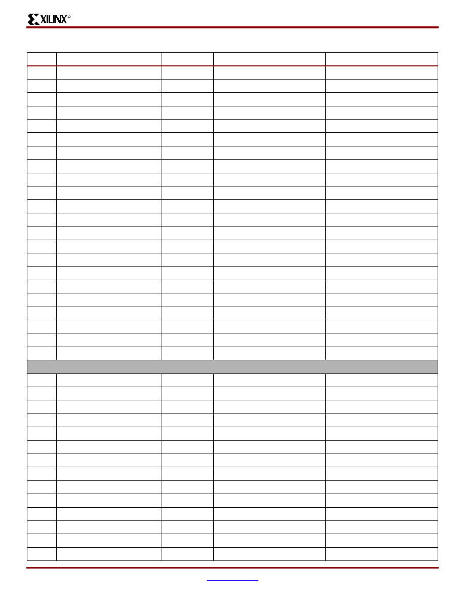
VirtexTM-II Platform FPGAs: Pinout Information
R
DS031-4 (v2.0) August 1, 2003
www.xilinx.com
Module 4 of 4
Product Specification
1-800-255-7778
113
6
VCCO_6
AF29
6
VCCO_6
AA22
6
VCCO_6
Y22
6
VCCO_6
Y21
6
VCCO_6
W22
6
VCCO_6
W21
6
VCCO_6
V28
6
VCCO_6
V22
6
VCCO_6
V21
6
VCCO_6
U21
6
VCCO_6
T21
7
VCCO_7
R21
7
VCCO_7
P21
7
VCCO_7
N28
7
VCCO_7
N22
7
VCCO_7
N21
7
VCCO_7
M22
7
VCCO_7
M21
7
VCCO_7
L22
7
VCCO_7
L21
7
VCCO_7
K22
7
VCCO_7
E29
NA
CCLK
AF6
NA
PROG_B
B28
NA
DONE
AG5
NA
M0
AF25
NA
M1
AG26
NA
M2
AH27
NA
HSWAP_EN
C27
NA
TCK
D5
NA
TDI
A29
NA
TDO
B3
NA
TMS
C4
NA
PWRDWN_B
AH4
NA
DXN
D26
NA
DXP
E25
Table 11: FF896 BGA -- XC2V1000, XC2V1500, and XC2V2000
Bank
Pin Description
Pin Number
No Connect in the XC2V1000
No Connect in the XC2V1500

VirtexTM-II Platform FPGAs: Pinout Information
R
DS031-4 (v2.0) August 1, 2003
www.xilinx.com
Module 4 of 4
Product Specification
1-800-255-7778
114
NA
VBATT
A2
NA
RSVD
E6
NA
VCCAUX
AK28
NA
VCCAUX
AK16
NA
VCCAUX
AK3
NA
VCCAUX
T1
NA
VCCAUX
R30
NA
VCCAUX
A28
NA
VCCAUX
A15
NA
VCCAUX
A3
NA
VCCINT
AB22
NA
VCCINT
AB9
NA
VCCINT
AA21
NA
VCCINT
AA10
NA
VCCINT
Y20
NA
VCCINT
Y19
NA
VCCINT
Y18
NA
VCCINT
Y17
NA
VCCINT
Y16
NA
VCCINT
Y15
NA
VCCINT
Y14
NA
VCCINT
Y13
NA
VCCINT
Y12
NA
VCCINT
Y11
NA
VCCINT
W20
NA
VCCINT
W11
NA
VCCINT
V20
NA
VCCINT
V11
NA
VCCINT
U20
NA
VCCINT
U11
NA
VCCINT
T20
NA
VCCINT
T11
NA
VCCINT
R20
NA
VCCINT
R11
NA
VCCINT
P20
NA
VCCINT
P11
Table 11: FF896 BGA -- XC2V1000, XC2V1500, and XC2V2000
Bank
Pin Description
Pin Number
No Connect in the XC2V1000
No Connect in the XC2V1500

VirtexTM-II Platform FPGAs: Pinout Information
R
DS031-4 (v2.0) August 1, 2003
www.xilinx.com
Module 4 of 4
Product Specification
1-800-255-7778
115
NA
VCCINT
N20
NA
VCCINT
N11
NA
VCCINT
M20
NA
VCCINT
M11
NA
VCCINT
L20
NA
VCCINT
L19
NA
VCCINT
L18
NA
VCCINT
L17
NA
VCCINT
L16
NA
VCCINT
L15
NA
VCCINT
L14
NA
VCCINT
L13
NA
VCCINT
L12
NA
VCCINT
L11
NA
VCCINT
K21
NA
VCCINT
K10
NA
VCCINT
J22
NA
VCCINT
J9
NA
GND
AK23
NA
GND
AK8
NA
GND
AJ29
NA
GND
AJ2
NA
GND
AH28
NA
GND
AH21
NA
GND
AH10
NA
GND
AH3
NA
GND
AG27
NA
GND
AG4
NA
GND
AF26
NA
GND
AF19
NA
GND
AF12
NA
GND
AF5
NA
GND
AE25
NA
GND
AE6
NA
GND
AD17
NA
GND
AD14
NA
GND
AC30
Table 11: FF896 BGA -- XC2V1000, XC2V1500, and XC2V2000
Bank
Pin Description
Pin Number
No Connect in the XC2V1000
No Connect in the XC2V1500
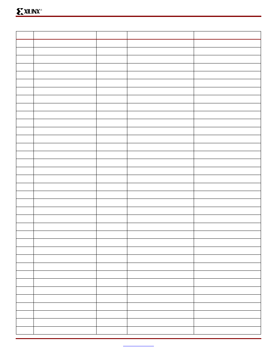
VirtexTM-II Platform FPGAs: Pinout Information
R
DS031-4 (v2.0) August 1, 2003
www.xilinx.com
Module 4 of 4
Product Specification
1-800-255-7778
116
NA
GND
AC1
NA
GND
AA28
NA
GND
AA3
NA
GND
W26
NA
GND
W19
NA
GND
W18
NA
GND
W17
NA
GND
W16
NA
GND
W15
NA
GND
W14
NA
GND
W13
NA
GND
W12
NA
GND
W5
NA
GND
V19
NA
GND
V18
NA
GND
V17
NA
GND
V16
NA
GND
V15
NA
GND
V14
NA
GND
V13
NA
GND
V12
NA
GND
U24
NA
GND
U19
NA
GND
U18
NA
GND
U17
NA
GND
U16
NA
GND
U15
NA
GND
U14
NA
GND
U13
NA
GND
U12
NA
GND
U7
NA
GND
T19
NA
GND
T18
NA
GND
T17
NA
GND
T16
NA
GND
T15
NA
GND
T14
Table 11: FF896 BGA -- XC2V1000, XC2V1500, and XC2V2000
Bank
Pin Description
Pin Number
No Connect in the XC2V1000
No Connect in the XC2V1500

VirtexTM-II Platform FPGAs: Pinout Information
R
DS031-4 (v2.0) August 1, 2003
www.xilinx.com
Module 4 of 4
Product Specification
1-800-255-7778
117
NA
GND
T13
NA
GND
T12
NA
GND
R19
NA
GND
R18
NA
GND
R17
NA
GND
R16
NA
GND
R15
NA
GND
R14
NA
GND
R13
NA
GND
R12
NA
GND
P24
NA
GND
P19
NA
GND
P18
NA
GND
P17
NA
GND
P16
NA
GND
P15
NA
GND
P14
NA
GND
P13
NA
GND
P12
NA
GND
P7
NA
GND
N19
NA
GND
N18
NA
GND
N17
NA
GND
N16
NA
GND
N15
NA
GND
N14
NA
GND
N13
NA
GND
N12
NA
GND
M26
NA
GND
M19
NA
GND
M18
NA
GND
M17
NA
GND
M16
NA
GND
M15
NA
GND
M14
NA
GND
M13
NA
GND
M12
Table 11: FF896 BGA -- XC2V1000, XC2V1500, and XC2V2000
Bank
Pin Description
Pin Number
No Connect in the XC2V1000
No Connect in the XC2V1500
VirtexTM-II Platform FPGAs: Pinout Information
R
DS031-4 (v2.0) August 1, 2003
www.xilinx.com
Module 4 of 4
Product Specification
1-800-255-7778
118
NA
GND
M5
NA
GND
K28
NA
GND
K3
NA
GND
H30
NA
GND
H1
NA
GND
G17
NA
GND
G14
NA
GND
F25
NA
GND
F6
NA
GND
E26
NA
GND
E19
NA
GND
E12
NA
GND
E5
NA
GND
D27
NA
GND
D4
NA
GND
C28
NA
GND
C21
NA
GND
C10
NA
GND
C3
NA
GND
B29
NA
GND
B2
NA
GND
A23
NA
GND
A8
Notes:
1.
See
Table 4
for an explanation of the signals available on this pin.
Table 11: FF896 BGA -- XC2V1000, XC2V1500, and XC2V2000
Bank
Pin Description
Pin Number
No Connect in the XC2V1000
No Connect in the XC2V1500

VirtexTM-II Platform FPGAs: Pinout Information
R
DS031-4 (v2.0) August 1, 2003
www.xilinx.com
Module 4 of 4
Product Specification
1-800-255-7778
119
FF896 Flip-Chip Fine-Pitch BGA Package Specifications (1.00mm pitch)
Figure 7: FF896 Flip-Chip Fine-Pitch BGA Package Specifications

VirtexTM-II Platform FPGAs: Pinout Information
R
DS031-4 (v2.0) August 1, 2003
www.xilinx.com
Module 4 of 4
Product Specification
1-800-255-7778
120
FF1152 Flip-Chip Fine-Pitch BGA Package
As shown in
Table 12
, XC2V3000, XC2V4000, XC2V6000, and XC2V8000 Virtex-II devices are available in the FF1152
flip-chip fine-pitch BGA package. Pins in each of these devices are the same, except for the pin differences in the XC2V3000
device shown in the No Connect column. Following this table are the
FF1152 Flip-Chip Fine-Pitch BGA Package
Specifications (1.00mm pitch)
.
Table 12: FF1152 BGA -- XC2V3000, XC2V4000, XC2V6000, and XC2V8000
Bank
Pin Description
Pin Number
No Connect in the XC2V3000
0
IO_L01N_0
D29
0
IO_L01P_0
C29
0
IO_L02N_0
H26
0
IO_L02P_0
G26
0
IO_L03N_0/VRP_0
E28
0
IO_L03P_0/VRN_0
E27
0
IO_L04N_0/VREF_0
F25
0
IO_L04P_0
F26
0
IO_L05N_0
H25
0
IO_L05P_0
H24
0
IO_L06N_0
E26
0
IO_L06P_0
F27
0
IO_L19N_0
B32
0
IO_L19P_0
C33
0
IO_L20N_0
J24
0
IO_L20P_0
J23
0
IO_L21N_0
C27
0
IO_L21P_0/VREF_0
C28
0
IO_L22N_0
B30
0
IO_L22P_0
B31
0
IO_L23N_0
K23
0
IO_L23P_0
K22
0
IO_L24N_0
C26
0
IO_L24P_0
D27
0
IO_L25N_0
A30
0
IO_L25P_0
A31
0
IO_L26N_0
G24
0
IO_L26P_0
G25
0
IO_L27N_0
E25
0
IO_L27P_0/VREF_0
E24
0
IO_L28N_0
D25

VirtexTM-II Platform FPGAs: Pinout Information
R
DS031-4 (v2.0) August 1, 2003
www.xilinx.com
Module 4 of 4
Product Specification
1-800-255-7778
121
0
IO_L28P_0
D26
0
IO_L29N_0
H23
0
IO_L29P_0
H22
0
IO_L30N_0
F23
0
IO_L30P_0
F24
0
IO_L49N_0
B28
0
IO_L49P_0
B29
0
IO_L50N_0
J22
0
IO_L50P_0
J21
0
IO_L51N_0
A28
0
IO_L51P_0/VREF_0
A29
0
IO_L52N_0
A26
0
IO_L52P_0
B27
0
IO_L53N_0
C24
0
IO_L53P_0
D24
0
IO_L54N_0
D22
0
IO_L54P_0
D23
0
IO_L60N_0
B25
NC
0
IO_L60P_0
B26
NC
0
IO_L67N_0
B23
0
IO_L67P_0
B24
0
IO_L68N_0
G22
0
IO_L68P_0
G23
0
IO_L69N_0
F22
0
IO_L69P_0/VREF_0
F21
0
IO_L70N_0
A23
0
IO_L70P_0
A24
0
IO_L71N_0
K21
0
IO_L71P_0
K20
0
IO_L72N_0
C22
0
IO_L72P_0
C23
0
IO_L73N_0
E21
0
IO_L73P_0
E22
0
IO_L74N_0
H21
0
IO_L74P_0
H20
0
IO_L75N_0
G20
Table 12: FF1152 BGA -- XC2V3000, XC2V4000, XC2V6000, and XC2V8000
Bank
Pin Description
Pin Number
No Connect in the XC2V3000

VirtexTM-II Platform FPGAs: Pinout Information
R
DS031-4 (v2.0) August 1, 2003
www.xilinx.com
Module 4 of 4
Product Specification
1-800-255-7778
122
0
IO_L75P_0/VREF_0
F20
0
IO_L76N_0
B21
0
IO_L76P_0
B22
0
IO_L77N_0
J20
0
IO_L77P_0
K19
0
IO_L78N_0
D20
0
IO_L78P_0
D21
0
IO_L79N_0
A21
NC
0
IO_L79P_0
A22
NC
0
IO_L80N_0
L19
NC
0
IO_L80P_0
L18
NC
0
IO_L81N_0
B19
NC
0
IO_L81P_0/VREF_0
A20
NC
0
IO_L82N_0
A18
NC
0
IO_L82P_0
B18
NC
0
IO_L83N_0
H19
NC
0
IO_L83P_0
H18
NC
0
IO_L84N_0
C20
NC
0
IO_L84P_0
C21
NC
0
IO_L91N_0/VREF_0
D19
0
IO_L91P_0
D18
0
IO_L92N_0
G18
0
IO_L92P_0
G19
0
IO_L93N_0
F18
0
IO_L93P_0
F19
0
IO_L94N_0/VREF_0
C19
0
IO_L94P_0
C18
0
IO_L95N_0/GCLK7P
K18
0
IO_L95P_0/GCLK6S
J18
0
IO_L96N_0/GCLK5P
E19
0
IO_L96P_0/GCLK4S
E18
1
IO_L96N_1/GCLK3P
E17
1
IO_L96P_1/GCLK2S
E16
1
IO_L95N_1/GCLK1P
H17
1
IO_L95P_1/GCLK0S
H16
Table 12: FF1152 BGA -- XC2V3000, XC2V4000, XC2V6000, and XC2V8000
Bank
Pin Description
Pin Number
No Connect in the XC2V3000

VirtexTM-II Platform FPGAs: Pinout Information
R
DS031-4 (v2.0) August 1, 2003
www.xilinx.com
Module 4 of 4
Product Specification
1-800-255-7778
123
1
IO_L94N_1
D17
1
IO_L94P_1/VREF_1
D16
1
IO_L93N_1
F16
1
IO_L93P_1
F17
1
IO_L92N_1
G16
1
IO_L92P_1
G17
1
IO_L91N_1
C16
1
IO_L91P_1/VREF_1
C15
1
IO_L84N_1
D14
NC
1
IO_L84P_1
D15
NC
1
IO_L83N_1
J17
NC
1
IO_L83P_1
K17
NC
1
IO_L82N_1
B17
NC
1
IO_L82P_1
A17
NC
1
IO_L81N_1/VREF_1
A15
NC
1
IO_L81P_1
B16
NC
1
IO_L80N_1
L17
NC
1
IO_L80P_1
L16
NC
1
IO_L79N_1
A13
NC
1
IO_L79P_1
A14
NC
1
IO_L78N_1
C13
1
IO_L78P_1
C14
1
IO_L77N_1
K16
1
IO_L77P_1
K15
1
IO_L76N_1
B13
1
IO_L76P_1
B14
1
IO_L75N_1/VREF_1
F15
1
IO_L75P_1
G15
1
IO_L74N_1
H15
1
IO_L74P_1
H14
1
IO_L73N_1
A11
1
IO_L73P_1
A12
1
IO_L72N_1
E13
1
IO_L72P_1
E14
1
IO_L71N_1
J15
1
IO_L71P_1
J14
Table 12: FF1152 BGA -- XC2V3000, XC2V4000, XC2V6000, and XC2V8000
Bank
Pin Description
Pin Number
No Connect in the XC2V3000

VirtexTM-II Platform FPGAs: Pinout Information
R
DS031-4 (v2.0) August 1, 2003
www.xilinx.com
Module 4 of 4
Product Specification
1-800-255-7778
124
1
IO_L70N_1
D12
1
IO_L70P_1
D13
1
IO_L69N_1/VREF_1
F14
1
IO_L69P_1
F13
1
IO_L68N_1
C11
1
IO_L68P_1
C12
1
IO_L67N_1
B11
1
IO_L67P_1
B12
1
IO_L60N_1
F11
NC
1
IO_L60P_1
F12
NC
1
IO_L54N_1
D10
1
IO_L54P_1
D11
1
IO_L53N_1
G12
1
IO_L53P_1
G13
1
IO_L52N_1
B9
1
IO_L52P_1
B10
1
IO_L51N_1/VREF_1
B8
1
IO_L51P_1
A9
1
IO_L50N_1
K14
1
IO_L50P_1
K13
1
IO_L49N_1
A6
1
IO_L49P_1
A7
1
IO_L30N_1
D9
1
IO_L30P_1
C9
1
IO_L29N_1
H13
1
IO_L29P_1
H12
1
IO_L28N_1
C7
1
IO_L28P_1
C8
1
IO_L27N_1/VREF_1
E11
1
IO_L27P_1
E10
1
IO_L26N_1
J13
1
IO_L26P_1
K12
1
IO_L25N_1
B6
1
IO_L25P_1
B7
1
IO_L24N_1
E8
1
IO_L24P_1
E9
Table 12: FF1152 BGA -- XC2V3000, XC2V4000, XC2V6000, and XC2V8000
Bank
Pin Description
Pin Number
No Connect in the XC2V3000
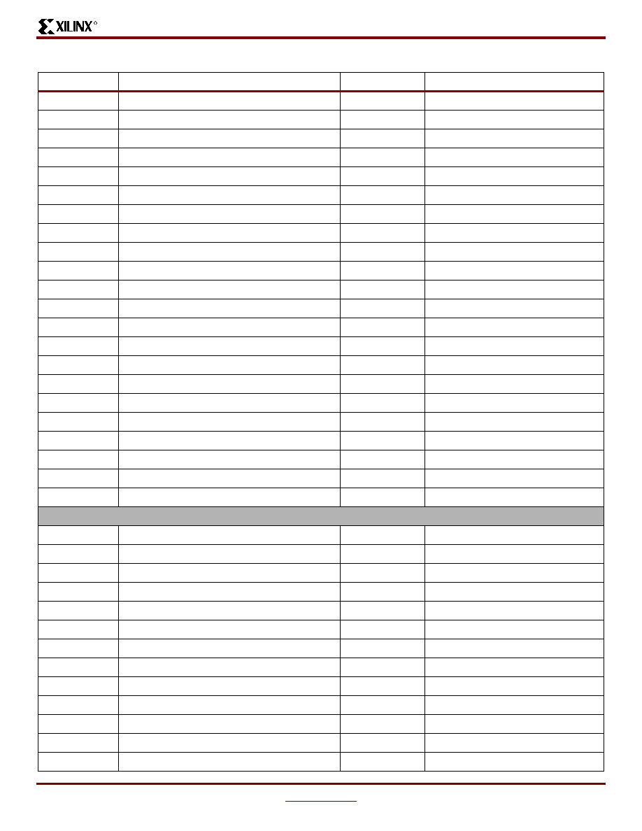
VirtexTM-II Platform FPGAs: Pinout Information
R
DS031-4 (v2.0) August 1, 2003
www.xilinx.com
Module 4 of 4
Product Specification
1-800-255-7778
125
1
IO_L23N_1
G10
1
IO_L23P_1
G11
1
IO_L22N_1
A4
1
IO_L22P_1
A5
1
IO_L21N_1/VREF_1
F10
1
IO_L21P_1
G9
1
IO_L20N_1
J12
1
IO_L20P_1
J11
1
IO_L19N_1
B4
1
IO_L19P_1
B5
1
IO_L06N_1
D6
1
IO_L06P_1
C6
1
IO_L05N_1
H11
1
IO_L05P_1
J10
1
IO_L04N_1
D8
1
IO_L04P_1/VREF_1
E7
1
IO_L03N_1/VRP_1
F9
1
IO_L03P_1/VRN_1
F8
1
IO_L02N_1
H10
1
IO_L02P_1
H9
1
IO_L01N_1
C2
1
IO_L01P_1
B3
2
IO_L01N_2
E2
2
IO_L01P_2
D2
2
IO_L02N_2/VRP_2
K11
2
IO_L02P_2/VRN_2
K10
2
IO_L03N_2
F5
2
IO_L03P_2/VREF_2
G5
2
IO_L04N_2
E3
2
IO_L04P_2
D3
2
IO_L05N_2
J9
2
IO_L05P_2
K9
2
IO_L06N_2
F4
2
IO_L06P_2
E4
2
IO_L19N_2
E1
Table 12: FF1152 BGA -- XC2V3000, XC2V4000, XC2V6000, and XC2V8000
Bank
Pin Description
Pin Number
No Connect in the XC2V3000

VirtexTM-II Platform FPGAs: Pinout Information
R
DS031-4 (v2.0) August 1, 2003
www.xilinx.com
Module 4 of 4
Product Specification
1-800-255-7778
126
2
IO_L19P_2
D1
2
IO_L20N_2
J8
2
IO_L20P_2
K8
2
IO_L21N_2
H7
2
IO_L21P_2/VREF_2
J7
2
IO_L22N_2
H6
2
IO_L22P_2
G6
2
IO_L23N_2
L10
2
IO_L23P_2
L9
2
IO_L24N_2
G3
2
IO_L24P_2
F3
2
IO_L25N_2
G2
2
IO_L25P_2
F2
2
IO_L26N_2
M10
2
IO_L26P_2
N10
2
IO_L27N_2
J6
2
IO_L27P_2/VREF_2
K6
2
IO_L28N_2
J5
2
IO_L28P_2
H5
2
IO_L29N_2
L7
2
IO_L29P_2
K7
2
IO_L30N_2
J4
2
IO_L30P_2
H4
2
IO_L43N_2
G1
2
IO_L43P_2
F1
2
IO_L44N_2
L8
2
IO_L44P_2
M8
2
IO_L45N_2
J1
2
IO_L45P_2/VREF_2
H2
2
IO_L46N_2
J3
2
IO_L46P_2
H3
2
IO_L47N_2
M9
2
IO_L47P_2
N9
2
IO_L48N_2
L5
2
IO_L48P_2
K5
2
IO_L49N_2
K2
Table 12: FF1152 BGA -- XC2V3000, XC2V4000, XC2V6000, and XC2V8000
Bank
Pin Description
Pin Number
No Connect in the XC2V3000

VirtexTM-II Platform FPGAs: Pinout Information
R
DS031-4 (v2.0) August 1, 2003
www.xilinx.com
Module 4 of 4
Product Specification
1-800-255-7778
127
2
IO_L49P_2
J2
2
IO_L50N_2
N7
2
IO_L50P_2
M7
2
IO_L51N_2
L6
2
IO_L51P_2/VREF_2
M6
2
IO_L52N_2
M3
2
IO_L52P_2
L3
2
IO_L53N_2
L4
2
IO_L53P_2
K4
2
IO_L54N_2
N4
2
IO_L54P_2
M4
2
IO_L67N_2
M2
2
IO_L67P_2
L2
2
IO_L68N_2
N8
2
IO_L68P_2
P8
2
IO_L69N_2
N6
2
IO_L69P_2/VREF_2
P6
2
IO_L70N_2
P5
2
IO_L70P_2
N5
2
IO_L71N_2
P10
2
IO_L71P_2
R10
2
IO_L72N_2
P3
2
IO_L72P_2
N3
2
IO_L73N_2
M1
2
IO_L73P_2
L1
2
IO_L74N_2
P9
2
IO_L74P_2
R9
2
IO_L75N_2
P2
2
IO_L75P_2/VREF_2
N2
2
IO_L76N_2
R4
2
IO_L76P_2
P4
2
IO_L77N_2
R8
2
IO_L77P_2
T8
2
IO_L78N_2
T3
2
IO_L78P_2
R3
2
IO_L79N_2
P1
NC
Table 12: FF1152 BGA -- XC2V3000, XC2V4000, XC2V6000, and XC2V8000
Bank
Pin Description
Pin Number
No Connect in the XC2V3000
VirtexTM-II Platform FPGAs: Pinout Information
R
DS031-4 (v2.0) August 1, 2003
www.xilinx.com
Module 4 of 4
Product Specification
1-800-255-7778
128
2
IO_L79P_2
N1
NC
2
IO_L80N_2
T11
NC
2
IO_L80P_2
U11
NC
2
IO_L81N_2
R7
NC
2
IO_L81P_2/VREF_2
R6
NC
2
IO_L82N_2
U5
NC
2
IO_L82P_2
T5
NC
2
IO_L83N_2
T10
NC
2
IO_L83P_2
U10
NC
2
IO_L84N_2
U4
NC
2
IO_L84P_2
T4
NC
2
IO_L91N_2
T2
2
IO_L91P_2
R1
2
IO_L92N_2
U7
2
IO_L92P_2
T7
2
IO_L93N_2
T6
2
IO_L93P_2/VREF_2
U6
2
IO_L94N_2
U1
2
IO_L94P_2
U2
2
IO_L95N_2
U9
2
IO_L95P_2
U8
2
IO_L96N_2
U3
2
IO_L96P_2
V4
3
IO_L96N_3
V6
3
IO_L96P_3
W6
3
IO_L95N_3
V5
3
IO_L95P_3
W5
3
IO_L94N_3
V7
3
IO_L94P_3
W7
3
IO_L93N_3/VREF_3
V10
3
IO_L93P_3
W10
3
IO_L92N_3
V1
3
IO_L92P_3
V2
3
IO_L91N_3
W3
3
IO_L91P_3
Y3
Table 12: FF1152 BGA -- XC2V3000, XC2V4000, XC2V6000, and XC2V8000
Bank
Pin Description
Pin Number
No Connect in the XC2V3000

VirtexTM-II Platform FPGAs: Pinout Information
R
DS031-4 (v2.0) August 1, 2003
www.xilinx.com
Module 4 of 4
Product Specification
1-800-255-7778
129
3
IO_L84N_3
V9
NC
3
IO_L84P_3
V8
NC
3
IO_L83N_3
W4
NC
3
IO_L83P_3
Y4
NC
3
IO_L82N_3
W11
NC
3
IO_L82P_3
V11
NC
3
IO_L81N_3/VREF_3
W8
NC
3
IO_L81P_3
Y8
NC
3
IO_L80N_3
W2
NC
3
IO_L80P_3
Y1
NC
3
IO_L79N_3
AA3
NC
3
IO_L79P_3
AB3
NC
3
IO_L78N_3
Y6
3
IO_L78P_3
AA6
3
IO_L77N_3
AA4
3
IO_L77P_3
AB4
3
IO_L76N_3
Y7
3
IO_L76P_3
AA8
3
IO_L75N_3/VREF_3
Y10
3
IO_L75P_3
AA10
3
IO_L74N_3
AA1
3
IO_L74P_3
AB1
3
IO_L73N_3
AA5
3
IO_L73P_3
AB5
3
IO_L72N_3
AA9
3
IO_L72P_3
Y9
3
IO_L71N_3
AA2
3
IO_L71P_3
AB2
3
IO_L70N_3
AB6
3
IO_L70P_3
AC6
3
IO_L69N_3/VREF_3
AD1
3
IO_L69P_3
AC1
3
IO_L68N_3
AC3
3
IO_L68P_3
AD3
3
IO_L67N_3
AC4
3
IO_L67P_3
AD4
Table 12: FF1152 BGA -- XC2V3000, XC2V4000, XC2V6000, and XC2V8000
Bank
Pin Description
Pin Number
No Connect in the XC2V3000

VirtexTM-II Platform FPGAs: Pinout Information
R
DS031-4 (v2.0) August 1, 2003
www.xilinx.com
Module 4 of 4
Product Specification
1-800-255-7778
130
3
IO_L54N_3
AB7
3
IO_L54P_3
AC7
3
IO_L53N_3
AC2
3
IO_L53P_3
AD2
3
IO_L52N_3
AC8
3
IO_L52P_3
AB8
3
IO_L51N_3/VREF_3
AB10
3
IO_L51P_3
AC10
3
IO_L50N_3
AD5
3
IO_L50P_3
AE5
3
IO_L49N_3
AE4
3
IO_L49P_3
AF4
3
IO_L48N_3
AB9
3
IO_L48P_3
AC9
3
IO_L47N_3
AE2
3
IO_L47P_3
AF1
3
IO_L46N_3
AD6
3
IO_L46P_3
AE6
3
IO_L45N_3/VREF_3
AD9
3
IO_L45P_3
AE9
3
IO_L44N_3
AF2
3
IO_L44P_3
AG2
3
IO_L43N_3
AF3
3
IO_L43P_3
AG3
3
IO_L30N_3
AD7
3
IO_L30P_3
AE7
3
IO_L29N_3
AF5
3
IO_L29P_3
AG5
3
IO_L28N_3
AE8
3
IO_L28P_3
AD8
3
IO_L27N_3/VREF_3
AF8
3
IO_L27P_3
AF9
3
IO_L26N_3
AH1
3
IO_L26P_3
AJ1
3
IO_L25N_3
AG4
3
IO_L25P_3
AH5
Table 12: FF1152 BGA -- XC2V3000, XC2V4000, XC2V6000, and XC2V8000
Bank
Pin Description
Pin Number
No Connect in the XC2V3000

VirtexTM-II Platform FPGAs: Pinout Information
R
DS031-4 (v2.0) August 1, 2003
www.xilinx.com
Module 4 of 4
Product Specification
1-800-255-7778
131
3
IO_L24N_3
AF6
3
IO_L24P_3
AG6
3
IO_L23N_3
AH3
3
IO_L23P_3
AJ3
3
IO_L22N_3
AF7
3
IO_L22P_3
AG7
3
IO_L21N_3/VREF_3
AL1
3
IO_L21P_3
AK1
3
IO_L20N_3
AH2
3
IO_L20P_3
AJ2
3
IO_L19N_3
AJ4
3
IO_L19P_3
AK4
3
IO_L06N_3
AE10
3
IO_L06P_3
AD10
3
IO_L05N_3
AK2
3
IO_L05P_3
AL2
3
IO_L04N_3
AH6
3
IO_L04P_3
AJ5
3
IO_L03N_3/VREF_3
AE11
3
IO_L03P_3
AF11
3
IO_L02N_3/VRP_3
AK3
3
IO_L02P_3/VRN_3
AL3
3
IO_L01N_3
AF10
3
IO_L01P_3
AG9
4
IO_L01N_4/BUSY/DOUT
(1)
AM4
4
IO_L01P_4/INIT_B
AL5
4
IO_L02N_4/D0/DIN
(1)
AG10
4
IO_L02P_4/D1
AH11
4
IO_L03N_4/D2/ALT_VRP_4
AK7
4
IO_L03P_4/D3/ALT_VRN_4
AK8
4
IO_L04N_4/VREF_4
AL6
4
IO_L04P_4
AM6
4
IO_L05N_4/VRP_4
AK9
4
IO_L05P_4/VRN_4
AJ8
4
IO_L06N_4
AM8
Table 12: FF1152 BGA -- XC2V3000, XC2V4000, XC2V6000, and XC2V8000
Bank
Pin Description
Pin Number
No Connect in the XC2V3000

VirtexTM-II Platform FPGAs: Pinout Information
R
DS031-4 (v2.0) August 1, 2003
www.xilinx.com
Module 4 of 4
Product Specification
1-800-255-7778
132
4
IO_L06P_4
AM7
4
IO_L19N_4
AN3
4
IO_L19P_4
AM2
4
IO_L20N_4
AJ10
4
IO_L20P_4
AJ9
4
IO_L21N_4
AH9
4
IO_L21P_4/VREF_4
AH10
4
IO_L22N_4
AN5
4
IO_L22P_4
AN4
4
IO_L23N_4
AE12
4
IO_L23P_4
AE13
4
IO_L24N_4
AM9
4
IO_L24P_4
AL8
4
IO_L25N_4
AP5
4
IO_L25P_4
AP4
4
IO_L26N_4
AG11
4
IO_L26P_4
AG12
4
IO_L27N_4
AN7
4
IO_L27P_4/VREF_4
AN6
4
IO_L28N_4
AL10
4
IO_L28P_4
AL9
4
IO_L29N_4
AF12
4
IO_L29P_4
AF13
4
IO_L30N_4
AK10
4
IO_L30P_4
AK11
4
IO_L49N_4
AP7
4
IO_L49P_4
AP6
4
IO_L50N_4
AH13
4
IO_L50P_4
AH12
4
IO_L51N_4
AJ11
4
IO_L51P_4/VREF_4
AJ12
4
IO_L52N_4
AP9
4
IO_L52P_4
AN8
4
IO_L53N_4
AG13
4
IO_L53P_4
AG14
4
IO_L54N_4
AM11
Table 12: FF1152 BGA -- XC2V3000, XC2V4000, XC2V6000, and XC2V8000
Bank
Pin Description
Pin Number
No Connect in the XC2V3000

VirtexTM-II Platform FPGAs: Pinout Information
R
DS031-4 (v2.0) August 1, 2003
www.xilinx.com
Module 4 of 4
Product Specification
1-800-255-7778
133
4
IO_L54P_4
AL11
4
IO_L60N_4
AN10
NC
4
IO_L60P_4
AN9
NC
4
IO_L67N_4
AN12
4
IO_L67P_4
AN11
4
IO_L68N_4
AE14
4
IO_L68P_4
AE15
4
IO_L69N_4
AJ13
4
IO_L69P_4/VREF_4
AJ14
4
IO_L70N_4
AL13
4
IO_L70P_4
AL12
4
IO_L71N_4
AF14
4
IO_L71P_4
AF15
4
IO_L72N_4
AM13
4
IO_L72P_4
AM12
4
IO_L73N_4
AP12
4
IO_L73P_4
AP11
4
IO_L74N_4
AG15
4
IO_L74P_4
AG16
4
IO_L75N_4
AN14
4
IO_L75P_4/VREF_4
AN13
4
IO_L76N_4
AP14
4
IO_L76P_4
AP13
4
IO_L77N_4
AD16
4
IO_L77P_4
AD17
4
IO_L78N_4
AK14
4
IO_L78P_4
AK13
4
IO_L79N_4
AN16
NC
4
IO_L79P_4
AP15
NC
4
IO_L80N_4
AE16
NC
4
IO_L80P_4
AE17
NC
4
IO_L81N_4
AH15
NC
4
IO_L81P_4/VREF_4
AJ15
NC
4
IO_L82N_4
AP17
NC
4
IO_L82P_4
AN17
NC
4
IO_L83N_4
AH17
NC
Table 12: FF1152 BGA -- XC2V3000, XC2V4000, XC2V6000, and XC2V8000
Bank
Pin Description
Pin Number
No Connect in the XC2V3000
VirtexTM-II Platform FPGAs: Pinout Information
R
DS031-4 (v2.0) August 1, 2003
www.xilinx.com
Module 4 of 4
Product Specification
1-800-255-7778
134
4
IO_L83P_4
AH16
NC
4
IO_L84N_4
AL15
NC
4
IO_L84P_4
AL14
NC
4
IO_L91N_4/VREF_4
AL16
4
IO_L91P_4
AL17
4
IO_L92N_4
AJ17
4
IO_L92P_4
AJ16
4
IO_L93N_4
AM15
4
IO_L93P_4
AM14
4
IO_L94N_4/VREF_4
AM16
4
IO_L94P_4
AM17
4
IO_L95N_4/GCLK3S
AF17
4
IO_L95P_4/GCLK2P
AG17
4
IO_L96N_4/GCLK1S
AK16
4
IO_L96P_4/GCLK0P
AK17
5
IO_L96N_5/GCLK7S
AK18
5
IO_L96P_5/GCLK6P
AK19
5
IO_L95N_5/GCLK5S
AG18
5
IO_L95P_5/GCLK4P
AF18
5
IO_L94N_5
AL18
5
IO_L94P_5/VREF_5
AL19
5
IO_L93N_5
AJ19
5
IO_L93P_5
AJ18
5
IO_L92N_5
AH19
5
IO_L92P_5
AH18
5
IO_L91N_5
AM19
5
IO_L91P_5/VREF_5
AM20
5
IO_L84N_5
AL21
NC
5
IO_L84P_5
AL20
NC
5
IO_L83N_5
AM22
NC
5
IO_L83P_5
AM21
NC
5
IO_L82N_5
AN18
NC
5
IO_L82P_5
AP18
NC
5
IO_L81N_5/VREF_5
AP20
NC
5
IO_L81P_5
AN19
NC
Table 12: FF1152 BGA -- XC2V3000, XC2V4000, XC2V6000, and XC2V8000
Bank
Pin Description
Pin Number
No Connect in the XC2V3000

VirtexTM-II Platform FPGAs: Pinout Information
R
DS031-4 (v2.0) August 1, 2003
www.xilinx.com
Module 4 of 4
Product Specification
1-800-255-7778
135
5
IO_L80N_5
AE18
NC
5
IO_L80P_5
AE19
NC
5
IO_L79N_5
AP22
NC
5
IO_L79P_5
AP21
NC
5
IO_L78N_5
AK22
5
IO_L78P_5
AK21
5
IO_L77N_5
AD18
5
IO_L77P_5
AD19
5
IO_L76N_5
AN22
5
IO_L76P_5
AN21
5
IO_L75N_5/VREF_5
AJ20
5
IO_L75P_5
AH20
5
IO_L74N_5
AG19
5
IO_L74P_5
AG20
5
IO_L73N_5
AP24
5
IO_L73P_5
AP23
5
IO_L72N_5
AL23
5
IO_L72P_5
AL22
5
IO_L71N_5
AF20
5
IO_L71P_5
AF21
5
IO_L70N_5
AM24
5
IO_L70P_5
AM23
5
IO_L69N_5/VREF_5
AJ21
5
IO_L69P_5
AJ22
5
IO_L68N_5
AJ24
5
IO_L68P_5
AJ23
5
IO_L67N_5
AN24
5
IO_L67P_5
AN23
5
IO_L60N_5
AN26
NC
5
IO_L60P_5
AN25
NC
5
IO_L54N_5
AL25
5
IO_L54P_5
AL24
5
IO_L53N_5
AE20
5
IO_L53P_5
AE21
5
IO_L52N_5
AN27
5
IO_L52P_5
AP26
Table 12: FF1152 BGA -- XC2V3000, XC2V4000, XC2V6000, and XC2V8000
Bank
Pin Description
Pin Number
No Connect in the XC2V3000

VirtexTM-II Platform FPGAs: Pinout Information
R
DS031-4 (v2.0) August 1, 2003
www.xilinx.com
Module 4 of 4
Product Specification
1-800-255-7778
136
5
IO_L51N_5/VREF_5
AP29
5
IO_L51P_5
AP28
5
IO_L50N_5
AG21
5
IO_L50P_5
AG22
5
IO_L49N_5
AN29
5
IO_L49P_5
AN28
5
IO_L30N_5
AK24
5
IO_L30P_5
AK25
5
IO_L29N_5
AH23
5
IO_L29P_5
AH22
5
IO_L28N_5
AP31
5
IO_L28P_5
AP30
5
IO_L27N_5/VREF_5
AH24
5
IO_L27P_5
AH25
5
IO_L26N_5
AF22
5
IO_L26P_5
AF23
5
IO_L25N_5
AM27
5
IO_L25P_5
AM26
5
IO_L24N_5
AL27
5
IO_L24P_5
AL26
5
IO_L23N_5
AH26
5
IO_L23P_5
AJ25
5
IO_L22N_5
AN31
5
IO_L22P_5
AN30
5
IO_L21N_5/VREF_5
AK26
5
IO_L21P_5
AK27
5
IO_L20N_5
AG23
5
IO_L20P_5
AF24
5
IO_L19N_5
AM33
5
IO_L19P_5
AN32
5
IO_L06N_5
AJ27
5
IO_L06P_5
AJ26
5
IO_L05N_5/VRP_5
AE22
5
IO_L05P_5/VRN_5
AE23
5
IO_L04N_5
AM28
5
IO_L04P_5/VREF_5
AM29
Table 12: FF1152 BGA -- XC2V3000, XC2V4000, XC2V6000, and XC2V8000
Bank
Pin Description
Pin Number
No Connect in the XC2V3000
VirtexTM-II Platform FPGAs: Pinout Information
R
DS031-4 (v2.0) August 1, 2003
www.xilinx.com
Module 4 of 4
Product Specification
1-800-255-7778
137
5
IO_L03N_5/D4/ALT_VRP_5
AK28
5
IO_L03P_5/D5/ALT_VRN_5
AL29
5
IO_L02N_5/D6
AG24
5
IO_L02P_5/D7
AG25
5
IO_L01N_5/RDWR_B
AL30
5
IO_L01P_5/CS_B
AM31
6
IO_L01P_6
AE24
6
IO_L01N_6
AD25
6
IO_L02P_6/VRN_6
AJ30
6
IO_L02N_6/VRP_6
AH30
6
IO_L03P_6
AL32
6
IO_L03N_6/VREF_6
AK32
6
IO_L04P_6
AF25
6
IO_L04N_6
AE25
6
IO_L05P_6
AJ31
6
IO_L05N_6
AK31
6
IO_L06P_6
AH29
6
IO_L06N_6
AG29
6
IO_L19P_6
AG26
6
IO_L19N_6
AF26
6
IO_L20P_6
AL33
6
IO_L20N_6
AK33
6
IO_L21P_6
AJ32
6
IO_L21N_6/VREF_6
AH32
6
IO_L22P_6
AG28
6
IO_L22N_6
AF28
6
IO_L23P_6
AG30
6
IO_L23N_6
AF30
6
IO_L24P_6
AF29
6
IO_L24N_6
AE29
6
IO_L25P_6
AF27
6
IO_L25N_6
AE27
6
IO_L26P_6
AL34
6
IO_L26N_6
AK34
6
IO_L27P_6
AE28
Table 12: FF1152 BGA -- XC2V3000, XC2V4000, XC2V6000, and XC2V8000
Bank
Pin Description
Pin Number
No Connect in the XC2V3000

VirtexTM-II Platform FPGAs: Pinout Information
R
DS031-4 (v2.0) August 1, 2003
www.xilinx.com
Module 4 of 4
Product Specification
1-800-255-7778
138
6
IO_L27N_6/VREF_6
AD28
6
IO_L28P_6
AE26
6
IO_L28N_6
AD26
6
IO_L29P_6
AF31
6
IO_L29N_6
AG31
6
IO_L30P_6
AF32
6
IO_L30N_6
AG32
6
IO_L43P_6
AC25
6
IO_L43N_6
AB25
6
IO_L44P_6
AJ33
6
IO_L44N_6
AH33
6
IO_L45P_6
AE31
6
IO_L45N_6/VREF_6
AD32
6
IO_L46P_6
AD27
6
IO_L46N_6
AC27
6
IO_L47P_6
AJ34
6
IO_L47N_6
AH34
6
IO_L48P_6
AE30
6
IO_L48N_6
AD30
6
IO_L49P_6
AC26
6
IO_L49N_6
AB26
6
IO_L50P_6
AD29
6
IO_L50N_6
AC29
6
IO_L51P_6
AF33
6
IO_L51N_6/VREF_6
AG33
6
IO_L52P_6
AC28
6
IO_L52N_6
AB28
6
IO_L53P_6
AF34
6
IO_L53N_6
AE33
6
IO_L54P_6
AB27
6
IO_L54N_6
AA27
6
IO_L67P_6
AA25
6
IO_L67N_6
Y25
6
IO_L68P_6
AD33
6
IO_L68N_6
AC33
6
IO_L69P_6
AC32
Table 12: FF1152 BGA -- XC2V3000, XC2V4000, XC2V6000, and XC2V8000
Bank
Pin Description
Pin Number
No Connect in the XC2V3000

VirtexTM-II Platform FPGAs: Pinout Information
R
DS031-4 (v2.0) August 1, 2003
www.xilinx.com
Module 4 of 4
Product Specification
1-800-255-7778
139
6
IO_L69N_6/VREF_6
AB32
6
IO_L70P_6
AA26
6
IO_L70N_6
Y26
6
IO_L71P_6
AD34
6
IO_L71N_6
AC34
6
IO_L72P_6
AC31
6
IO_L72N_6
AD31
6
IO_L73P_6
Y27
6
IO_L73N_6
W27
6
IO_L74P_6
AB29
6
IO_L74N_6
AA29
6
IO_L75P_6
AB31
6
IO_L75N_6/VREF_6
AA31
6
IO_L76P_6
Y28
6
IO_L76N_6
Y29
6
IO_L77P_6
AB33
6
IO_L77N_6
AA33
6
IO_L78P_6
AA30
6
IO_L78N_6
AB30
6
IO_L79P_6
W24
NC
6
IO_L79N_6
V24
NC
6
IO_L80P_6
AB34
NC
6
IO_L80N_6
AA34
NC
6
IO_L81P_6
W33
NC
6
IO_L81N_6/VREF_6
Y34
NC
6
IO_L82P_6
W25
NC
6
IO_L82N_6
V25
NC
6
IO_L83P_6
Y32
NC
6
IO_L83N_6
AA32
NC
6
IO_L84P_6
W29
NC
6
IO_L84N_6
V29
NC
6
IO_L91P_6
W28
6
IO_L91N_6
V28
6
IO_L92P_6
V33
6
IO_L92N_6
V34
6
IO_L93P_6
Y31
Table 12: FF1152 BGA -- XC2V3000, XC2V4000, XC2V6000, and XC2V8000
Bank
Pin Description
Pin Number
No Connect in the XC2V3000
VirtexTM-II Platform FPGAs: Pinout Information
R
DS031-4 (v2.0) August 1, 2003
www.xilinx.com
Module 4 of 4
Product Specification
1-800-255-7778
140
6
IO_L93N_6/VREF_6
W31
6
IO_L94P_6
V26
6
IO_L94N_6
V27
6
IO_L95P_6
W30
6
IO_L95N_6
V30
6
IO_L96P_6
V32
6
IO_L96N_6
W32
7
IO_L96P_7
U31
7
IO_L96N_7
V31
7
IO_L95P_7
T28
7
IO_L95N_7
U28
7
IO_L94P_7
U33
7
IO_L94N_7
U34
7
IO_L93P_7/VREF_7
U29
7
IO_L93N_7
T29
7
IO_L92P_7
U27
7
IO_L92N_7
U26
7
IO_L91P_7
T30
7
IO_L91N_7
U30
7
IO_L84P_7
R32
NC
7
IO_L84N_7
T32
NC
7
IO_L83P_7
U25
NC
7
IO_L83N_7
T25
NC
7
IO_L82P_7
R34
NC
7
IO_L82N_7
T33
NC
7
IO_L81P_7/VREF_7
N34
NC
7
IO_L81N_7
P34
NC
7
IO_L80P_7
U24
NC
7
IO_L80N_7
T24
NC
7
IO_L79P_7
R31
NC
7
IO_L79N_7
T31
NC
7
IO_L78P_7
N32
7
IO_L78N_7
P32
7
IO_L77P_7
T27
7
IO_L77N_7
R27
Table 12: FF1152 BGA -- XC2V3000, XC2V4000, XC2V6000, and XC2V8000
Bank
Pin Description
Pin Number
No Connect in the XC2V3000

VirtexTM-II Platform FPGAs: Pinout Information
R
DS031-4 (v2.0) August 1, 2003
www.xilinx.com
Module 4 of 4
Product Specification
1-800-255-7778
141
7
IO_L76P_7
N33
7
IO_L76N_7
P33
7
IO_L75P_7/VREF_7
R29
7
IO_L75N_7
R28
7
IO_L74P_7
R26
7
IO_L74N_7
P26
7
IO_L73P_7
N31
7
IO_L73N_7
P31
7
IO_L72P_7
N30
7
IO_L72N_7
P30
7
IO_L71P_7
R25
7
IO_L71N_7
P25
7
IO_L70P_7
L34
7
IO_L70N_7
M34
7
IO_L69P_7/VREF_7
P29
7
IO_L69N_7
N29
7
IO_L68P_7
P27
7
IO_L68N_7
N27
7
IO_L67P_7
L32
7
IO_L67N_7
M32
7
IO_L54P_7
L31
7
IO_L54N_7
M31
7
IO_L53P_7
K29
7
IO_L53N_7
L30
7
IO_L52P_7
L33
7
IO_L52N_7
M33
7
IO_L51P_7/VREF_7
M29
7
IO_L51N_7
L29
7
IO_L50P_7
M28
7
IO_L50N_7
N28
7
IO_L49P_7
K30
7
IO_L49N_7
K31
7
IO_L48P_7
H32
7
IO_L48N_7
J32
7
IO_L47P_7
N26
7
IO_L47N_7
M26
Table 12: FF1152 BGA -- XC2V3000, XC2V4000, XC2V6000, and XC2V8000
Bank
Pin Description
Pin Number
No Connect in the XC2V3000

VirtexTM-II Platform FPGAs: Pinout Information
R
DS031-4 (v2.0) August 1, 2003
www.xilinx.com
Module 4 of 4
Product Specification
1-800-255-7778
142
7
IO_L46P_7
J33
7
IO_L46N_7
K33
7
IO_L45P_7/VREF_7
H33
7
IO_L45N_7
J34
7
IO_L44P_7
M27
7
IO_L44N_7
L27
7
IO_L43P_7
H31
7
IO_L43N_7
J31
7
IO_L30P_7
F32
7
IO_L30N_7
G32
7
IO_L29P_7
N25
7
IO_L29N_7
M25
7
IO_L28P_7
F34
7
IO_L28N_7
G34
7
IO_L27P_7/VREF_7
J30
7
IO_L27N_7
H30
7
IO_L26P_7
K28
7
IO_L26N_7
L28
7
IO_L25P_7
H28
7
IO_L25N_7
J29
7
IO_L24P_7
G29
7
IO_L24N_7
H29
7
IO_L23P_7
L26
7
IO_L23N_7
K26
7
IO_L22P_7
F33
7
IO_L22N_7
G33
7
IO_L21P_7/VREF_7
J28
7
IO_L21N_7
J27
7
IO_L20P_7
K27
7
IO_L20N_7
J26
7
IO_L19P_7
E31
7
IO_L19N_7
F31
7
IO_L06P_7
D32
7
IO_L06N_7
E32
7
IO_L05P_7
L25
7
IO_L05N_7
K24
Table 12: FF1152 BGA -- XC2V3000, XC2V4000, XC2V6000, and XC2V8000
Bank
Pin Description
Pin Number
No Connect in the XC2V3000

VirtexTM-II Platform FPGAs: Pinout Information
R
DS031-4 (v2.0) August 1, 2003
www.xilinx.com
Module 4 of 4
Product Specification
1-800-255-7778
143
7
IO_L04P_7
D34
7
IO_L04N_7
E34
7
IO_L03P_7/VREF_7
G30
7
IO_L03N_7
F30
7
IO_L02P_7/VRN_7
K25
7
IO_L02N_7/VRP_7
J25
7
IO_L01P_7
D33
7
IO_L01N_7
E33
0
VCCO_0
M22
0
VCCO_0
M21
0
VCCO_0
M20
0
VCCO_0
M19
0
VCCO_0
M18
0
VCCO_0
L23
0
VCCO_0
L22
0
VCCO_0
L21
0
VCCO_0
L20
0
VCCO_0
E20
0
VCCO_0
D28
0
VCCO_0
A25
0
VCCO_0
A19
1
VCCO_1
M17
1
VCCO_1
M16
1
VCCO_1
M15
1
VCCO_1
M14
1
VCCO_1
M13
1
VCCO_1
L15
1
VCCO_1
L14
1
VCCO_1
L13
1
VCCO_1
L12
1
VCCO_1
E15
1
VCCO_1
D7
1
VCCO_1
A16
1
VCCO_1
A10
2
VCCO_2
U12
Table 12: FF1152 BGA -- XC2V3000, XC2V4000, XC2V6000, and XC2V8000
Bank
Pin Description
Pin Number
No Connect in the XC2V3000
VirtexTM-II Platform FPGAs: Pinout Information
R
DS031-4 (v2.0) August 1, 2003
www.xilinx.com
Module 4 of 4
Product Specification
1-800-255-7778
144
2
VCCO_2
T12
2
VCCO_2
T1
2
VCCO_2
R12
2
VCCO_2
R11
2
VCCO_2
R5
2
VCCO_2
P12
2
VCCO_2
P11
2
VCCO_2
N12
2
VCCO_2
N11
2
VCCO_2
M11
2
VCCO_2
K1
2
VCCO_2
G4
3
VCCO_3
AH4
3
VCCO_3
AE1
3
VCCO_3
AC11
3
VCCO_3
AB12
3
VCCO_3
AB11
3
VCCO_3
AA12
3
VCCO_3
AA11
3
VCCO_3
Y12
3
VCCO_3
Y11
3
VCCO_3
Y5
3
VCCO_3
W12
3
VCCO_3
W1
3
VCCO_3
V12
4
VCCO_4
AP16
4
VCCO_4
AP10
4
VCCO_4
AL7
4
VCCO_4
AK15
4
VCCO_4
AD15
4
VCCO_4
AD14
4
VCCO_4
AD13
4
VCCO_4
AD12
4
VCCO_4
AC17
4
VCCO_4
AC16
4
VCCO_4
AC15
Table 12: FF1152 BGA -- XC2V3000, XC2V4000, XC2V6000, and XC2V8000
Bank
Pin Description
Pin Number
No Connect in the XC2V3000

VirtexTM-II Platform FPGAs: Pinout Information
R
DS031-4 (v2.0) August 1, 2003
www.xilinx.com
Module 4 of 4
Product Specification
1-800-255-7778
145
4
VCCO_4
AC14
4
VCCO_4
AC13
5
VCCO_5
AP25
5
VCCO_5
AP19
5
VCCO_5
AL28
5
VCCO_5
AK20
5
VCCO_5
AD23
5
VCCO_5
AD22
5
VCCO_5
AD21
5
VCCO_5
AD20
5
VCCO_5
AC22
5
VCCO_5
AC21
5
VCCO_5
AC20
5
VCCO_5
AC19
5
VCCO_5
AC18
6
VCCO_6
AH31
6
VCCO_6
AE34
6
VCCO_6
AC24
6
VCCO_6
AB24
6
VCCO_6
AB23
6
VCCO_6
AA24
6
VCCO_6
AA23
6
VCCO_6
Y30
6
VCCO_6
Y24
6
VCCO_6
Y23
6
VCCO_6
W34
6
VCCO_6
W23
6
VCCO_6
V23
7
VCCO_7
U23
7
VCCO_7
T34
7
VCCO_7
T23
7
VCCO_7
R30
7
VCCO_7
R24
7
VCCO_7
R23
7
VCCO_7
P24
7
VCCO_7
P23
Table 12: FF1152 BGA -- XC2V3000, XC2V4000, XC2V6000, and XC2V8000
Bank
Pin Description
Pin Number
No Connect in the XC2V3000
VirtexTM-II Platform FPGAs: Pinout Information
R
DS031-4 (v2.0) August 1, 2003
www.xilinx.com
Module 4 of 4
Product Specification
1-800-255-7778
146
7
VCCO_7
N24
7
VCCO_7
N23
7
VCCO_7
M24
7
VCCO_7
K34
7
VCCO_7
G31
NA
CCLK
AH8
NA
PROG_B
D30
NA
DONE
AJ7
NA
M0
AH27
NA
M1
AJ28
NA
M2
AK29
NA
HSWAP_EN
E29
NA
TCK
F7
NA
TDI
C31
NA
TDO
D5
NA
TMS
E6
NA
PWRDWN_B
AK6
NA
DXN
F28
NA
DXP
G27
NA
VBATT
C4
NA
RSVD
G8
NA
VCCAUX
AM30
NA
VCCAUX
AM18
NA
VCCAUX
AM5
NA
VCCAUX
V3
NA
VCCAUX
U32
NA
VCCAUX
C30
NA
VCCAUX
C17
NA
VCCAUX
C5
NA
VCCINT
AD24
NA
VCCINT
AD11
NA
VCCINT
AC23
NA
VCCINT
AC12
NA
VCCINT
AB22
NA
VCCINT
AB21
Table 12: FF1152 BGA -- XC2V3000, XC2V4000, XC2V6000, and XC2V8000
Bank
Pin Description
Pin Number
No Connect in the XC2V3000

VirtexTM-II Platform FPGAs: Pinout Information
R
DS031-4 (v2.0) August 1, 2003
www.xilinx.com
Module 4 of 4
Product Specification
1-800-255-7778
147
NA
VCCINT
AB20
NA
VCCINT
AB19
NA
VCCINT
AB18
NA
VCCINT
AB17
NA
VCCINT
AB16
NA
VCCINT
AB15
NA
VCCINT
AB14
NA
VCCINT
AB13
NA
VCCINT
AA22
NA
VCCINT
AA13
NA
VCCINT
Y22
NA
VCCINT
Y13
NA
VCCINT
W22
NA
VCCINT
W13
NA
VCCINT
V22
NA
VCCINT
V13
NA
VCCINT
U22
NA
VCCINT
U13
NA
VCCINT
T22
NA
VCCINT
T13
NA
VCCINT
R22
NA
VCCINT
R13
NA
VCCINT
P22
NA
VCCINT
P13
NA
VCCINT
N22
NA
VCCINT
N21
NA
VCCINT
N20
NA
VCCINT
N19
NA
VCCINT
N18
NA
VCCINT
N17
NA
VCCINT
N16
NA
VCCINT
N15
NA
VCCINT
N14
NA
VCCINT
N13
NA
VCCINT
M23
NA
VCCINT
M12
Table 12: FF1152 BGA -- XC2V3000, XC2V4000, XC2V6000, and XC2V8000
Bank
Pin Description
Pin Number
No Connect in the XC2V3000
VirtexTM-II Platform FPGAs: Pinout Information
R
DS031-4 (v2.0) August 1, 2003
www.xilinx.com
Module 4 of 4
Product Specification
1-800-255-7778
148
NA
VCCINT
L24
NA
VCCINT
L11
NA
GND
AP33
NA
GND
AP32
NA
GND
AP27
NA
GND
AP8
NA
GND
AP3
NA
GND
AP2
NA
GND
AN34
NA
GND
AN33
NA
GND
AN20
NA
GND
AN15
NA
GND
AN2
NA
GND
AN1
NA
GND
AM34
NA
GND
AM32
NA
GND
AM25
NA
GND
AM10
NA
GND
AM3
NA
GND
AM1
NA
GND
AL31
NA
GND
AL4
NA
GND
AK30
NA
GND
AK23
NA
GND
AK12
NA
GND
AK5
NA
GND
AJ29
NA
GND
AJ6
NA
GND
AH28
NA
GND
AH21
NA
GND
AH14
NA
GND
AH7
NA
GND
AG34
NA
GND
AG27
NA
GND
AG8
Table 12: FF1152 BGA -- XC2V3000, XC2V4000, XC2V6000, and XC2V8000
Bank
Pin Description
Pin Number
No Connect in the XC2V3000

VirtexTM-II Platform FPGAs: Pinout Information
R
DS031-4 (v2.0) August 1, 2003
www.xilinx.com
Module 4 of 4
Product Specification
1-800-255-7778
149
NA
GND
AG1
NA
GND
AF19
NA
GND
AF16
NA
GND
AE32
NA
GND
AE3
NA
GND
AC30
NA
GND
AC5
NA
GND
AA28
NA
GND
AA21
NA
GND
AA20
NA
GND
AA19
NA
GND
AA18
NA
GND
AA17
NA
GND
AA16
NA
GND
AA15
NA
GND
AA14
NA
GND
AA7
NA
GND
Y33
NA
GND
Y21
NA
GND
Y20
NA
GND
Y19
NA
GND
Y18
NA
GND
Y17
NA
GND
Y16
NA
GND
Y15
NA
GND
Y14
NA
GND
Y2
NA
GND
W26
NA
GND
W21
NA
GND
W20
NA
GND
W19
NA
GND
W18
NA
GND
W17
NA
GND
W16
NA
GND
W15
NA
GND
W14
Table 12: FF1152 BGA -- XC2V3000, XC2V4000, XC2V6000, and XC2V8000
Bank
Pin Description
Pin Number
No Connect in the XC2V3000

VirtexTM-II Platform FPGAs: Pinout Information
R
DS031-4 (v2.0) August 1, 2003
www.xilinx.com
Module 4 of 4
Product Specification
1-800-255-7778
150
NA
GND
W9
NA
GND
V21
NA
GND
V20
NA
GND
V19
NA
GND
V18
NA
GND
V17
NA
GND
V16
NA
GND
V15
NA
GND
V14
NA
GND
U21
NA
GND
U20
NA
GND
U19
NA
GND
U18
NA
GND
U17
NA
GND
U16
NA
GND
U15
NA
GND
U14
NA
GND
T26
NA
GND
T21
NA
GND
T20
NA
GND
T19
NA
GND
T18
NA
GND
T17
NA
GND
T16
NA
GND
T15
NA
GND
T14
NA
GND
T9
NA
GND
R33
NA
GND
R21
NA
GND
R20
NA
GND
R19
NA
GND
R18
NA
GND
R17
NA
GND
R16
NA
GND
R15
NA
GND
R14
Table 12: FF1152 BGA -- XC2V3000, XC2V4000, XC2V6000, and XC2V8000
Bank
Pin Description
Pin Number
No Connect in the XC2V3000

VirtexTM-II Platform FPGAs: Pinout Information
R
DS031-4 (v2.0) August 1, 2003
www.xilinx.com
Module 4 of 4
Product Specification
1-800-255-7778
151
NA
GND
R2
NA
GND
P28
NA
GND
P21
NA
GND
P20
NA
GND
P19
NA
GND
P18
NA
GND
P17
NA
GND
P16
NA
GND
P15
NA
GND
P14
NA
GND
P7
NA
GND
M30
NA
GND
M5
NA
GND
K32
NA
GND
K3
NA
GND
J19
NA
GND
J16
NA
GND
H34
NA
GND
H27
NA
GND
H8
NA
GND
H1
NA
GND
G28
NA
GND
G21
NA
GND
G14
NA
GND
G7
NA
GND
F29
NA
GND
F6
NA
GND
E30
NA
GND
E23
NA
GND
E12
NA
GND
E5
NA
GND
D31
NA
GND
D4
NA
GND
C34
NA
GND
C32
NA
GND
C25
Table 12: FF1152 BGA -- XC2V3000, XC2V4000, XC2V6000, and XC2V8000
Bank
Pin Description
Pin Number
No Connect in the XC2V3000
VirtexTM-II Platform FPGAs: Pinout Information
R
DS031-4 (v2.0) August 1, 2003
www.xilinx.com
Module 4 of 4
Product Specification
1-800-255-7778
152
NA
GND
C10
NA
GND
C3
NA
GND
C1
NA
GND
B34
NA
GND
B33
NA
GND
B20
NA
GND
B15
NA
GND
B2
NA
GND
B1
NA
GND
A33
NA
GND
A32
NA
GND
A27
NA
GND
A8
NA
GND
A3
NA
GND
A2
Notes:
1.
See
Table 4
for an explanation of the signals available on this pin.
Table 12: FF1152 BGA -- XC2V3000, XC2V4000, XC2V6000, and XC2V8000
Bank
Pin Description
Pin Number
No Connect in the XC2V3000
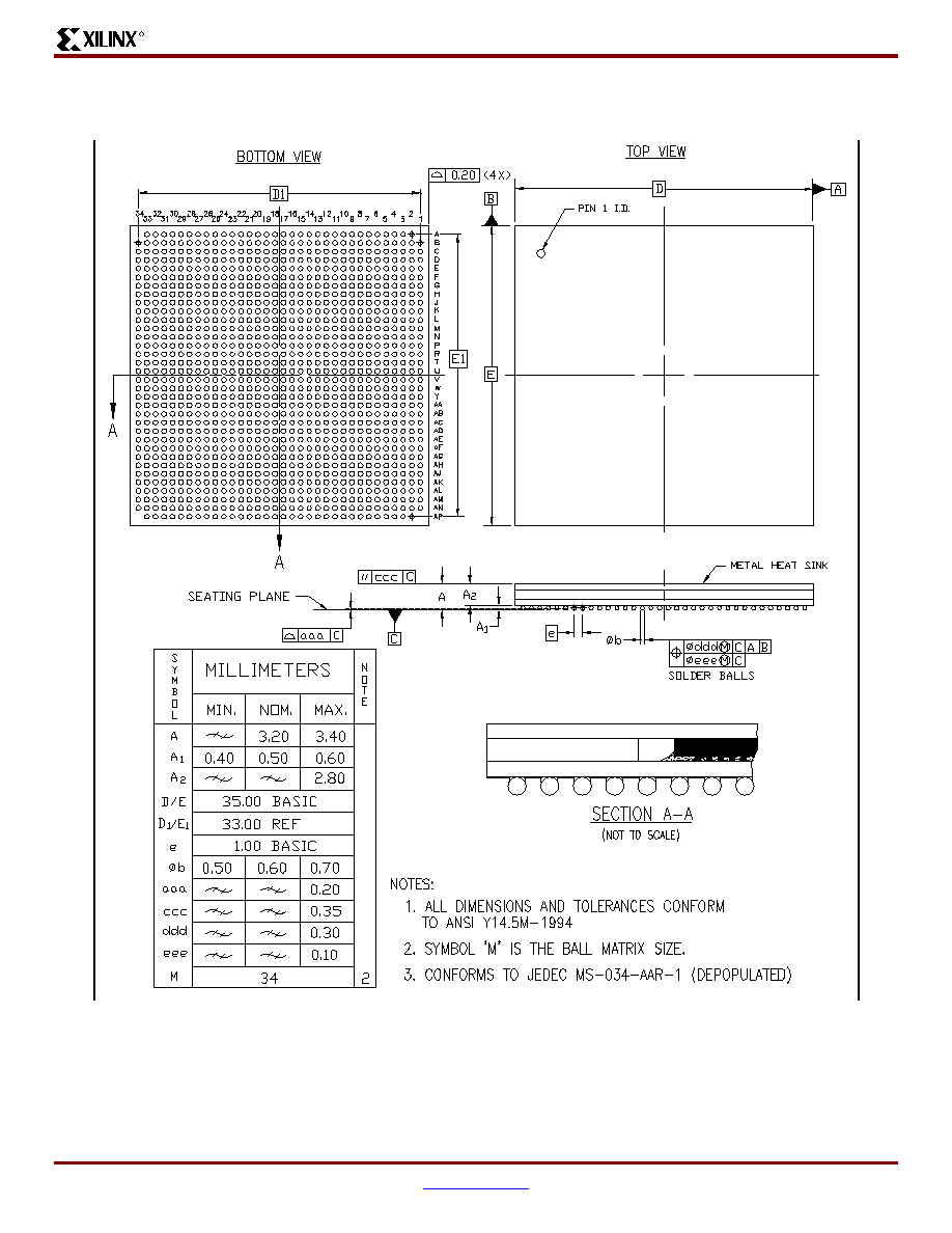
VirtexTM-II Platform FPGAs: Pinout Information
R
DS031-4 (v2.0) August 1, 2003
www.xilinx.com
Module 4 of 4
Product Specification
1-800-255-7778
153
FF1152 Flip-Chip Fine-Pitch BGA Package Specifications (1.00mm pitch)
Figure 8: FF1152 Flip-Chip Fine-Pitch BGA Package Specifications

VirtexTM-II Platform FPGAs: Pinout Information
R
DS031-4 (v2.0) August 1, 2003
www.xilinx.com
Module 4 of 4
Product Specification
1-800-255-7778
154
FF1517 Flip-Chip Fine-Pitch BGA Package
As shown in
Table 13
, XC2V4000, XC2V6000, and XC2V8000 Virtex-II devices are available in the FF1517 flip-chip
fine-pitch BGA package. Pins in each of these devices are the same, except for the pin differences in the XC2V4000 and
XC2V6000 devices shown in the No Connect columns. Following this table are the
FF1517 Flip-Chip Fine-Pitch BGA
Package Specifications (1.00mm pitch)
.
Table 13: FF1517 BGA -- XC2V4000, XC2V6000, and XC2V8000
Bank
Pin Description
Pin Number
No Connect in the XC2V4000
No Connect in the XC2V6000
0
IO_L01N_0
B36
0
IO_L01P_0
C36
0
IO_L02N_0
J30
0
IO_L02P_0
J29
0
IO_L03N_0/VRP_0
D33
0
IO_L03P_0/VRN_0
D34
0
IO_L04N_0/VREF_0
C34
0
IO_L04P_0
C35
0
IO_L05N_0
H30
0
IO_L05P_0
G30
0
IO_L06N_0
D32
0
IO_L06P_0
E33
0
IO_L07N_0
A35
NC
0
IO_L07P_0
A36
NC
0
IO_L08N_0
K28
NC
0
IO_L08P_0
J28
NC
0
IO_L09N_0
E32
NC
0
IO_L09P_0/VREF_0
F32
NC
0
IO_L10N_0
B34
NC
0
IO_L10P_0
B35
NC
0
IO_L11N_0
H29
NC
0
IO_L11P_0
H28
NC
0
IO_L12N_0
F31
NC
0
IO_L12P_0
G31
NC
0
IO_L19N_0
C32
0
IO_L19P_0
C33
0
IO_L20N_0
M26
0
IO_L20P_0
M25
0
IO_L21N_0
E30
0
IO_L21P_0/VREF_0
E31
0
IO_L22N_0
A33

VirtexTM-II Platform FPGAs: Pinout Information
R
DS031-4 (v2.0) August 1, 2003
www.xilinx.com
Module 4 of 4
Product Specification
1-800-255-7778
155
0
IO_L22P_0
A34
0
IO_L23N_0
K27
0
IO_L23P_0
K26
0
IO_L24N_0
F29
0
IO_L24P_0
F30
0
IO_L25N_0
B32
0
IO_L25P_0
B33
0
IO_L26N_0
L26
0
IO_L26P_0
L25
0
IO_L27N_0
G28
0
IO_L27P_0/VREF_0
G29
0
IO_L28N_0
C30
0
IO_L28P_0
C31
0
IO_L29N_0
J27
0
IO_L29P_0
J26
0
IO_L30N_0
D30
0
IO_L30P_0
D31
0
IO_L31N_0
A31
NC
0
IO_L31P_0
A32
NC
0
IO_L32N_0
H27
NC
0
IO_L32P_0
H26
NC
0
IO_L33N_0
F27
NC
0
IO_L33P_0/VREF_0
F28
NC
0
IO_L34N_0
B30
NC
0
IO_L34P_0
B31
NC
0
IO_L35N_0
M24
NC
0
IO_L35P_0
M23
NC
0
IO_L36N_0
D28
NC
0
IO_L36P_0
D29
NC
0
IO_L49N_0
C28
0
IO_L49P_0
C29
0
IO_L50N_0
K25
0
IO_L50P_0
L24
0
IO_L51N_0
E27
0
IO_L51P_0/VREF_0
E28
0
IO_L52N_0
A29
Table 13: FF1517 BGA -- XC2V4000, XC2V6000, and XC2V8000
Bank
Pin Description
Pin Number
No Connect in the XC2V4000
No Connect in the XC2V6000

VirtexTM-II Platform FPGAs: Pinout Information
R
DS031-4 (v2.0) August 1, 2003
www.xilinx.com
Module 4 of 4
Product Specification
1-800-255-7778
156
0
IO_L52P_0
A30
0
IO_L53N_0
G26
0
IO_L53P_0
G25
0
IO_L54N_0
D26
0
IO_L54P_0
D27
0
IO_L55N_0
B27
0
IO_L55P_0
B28
0
IO_L56N_0
H25
0
IO_L56P_0
H24
0
IO_L57N_0
F25
0
IO_L57P_0/VREF_0
F26
0
IO_L58N_0
A27
0
IO_L58P_0
A28
0
IO_L59N_0
K24
0
IO_L59P_0
K23
0
IO_L60N_0
E24
0
IO_L60P_0
E25
0
IO_L67N_0
C26
0
IO_L67P_0
C27
0
IO_L68N_0
J24
0
IO_L68P_0
J23
0
IO_L69N_0
D24
0
IO_L69P_0/VREF_0
D25
0
IO_L70N_0
A25
0
IO_L70P_0
A26
0
IO_L71N_0
M22
0
IO_L71P_0
M21
0
IO_L72N_0
G23
0
IO_L72P_0
G24
0
IO_L73N_0
B25
0
IO_L73P_0
C25
0
IO_L74N_0
L22
0
IO_L74P_0
L21
0
IO_L75N_0
F23
0
IO_L75P_0/VREF_0
F24
0
IO_L76N_0
C23
Table 13: FF1517 BGA -- XC2V4000, XC2V6000, and XC2V8000
Bank
Pin Description
Pin Number
No Connect in the XC2V4000
No Connect in the XC2V6000

VirtexTM-II Platform FPGAs: Pinout Information
R
DS031-4 (v2.0) August 1, 2003
www.xilinx.com
Module 4 of 4
Product Specification
1-800-255-7778
157
0
IO_L76P_0
C24
0
IO_L77N_0
K22
0
IO_L77P_0
K21
0
IO_L78N_0
E22
0
IO_L78P_0
E23
0
IO_L79N_0
B23
0
IO_L79P_0
B24
0
IO_L80N_0
J22
0
IO_L80P_0
J21
0
IO_L81N_0
G21
0
IO_L81P_0/VREF_0
G22
0
IO_L82N_0
A23
0
IO_L82P_0
A24
0
IO_L83N_0
H22
0
IO_L83P_0
H21
0
IO_L84N_0
F21
0
IO_L84P_0
F22
0
IO_L91N_0/VREF_0
B21
0
IO_L91P_0
B22
0
IO_L92N_0
L20
0
IO_L92P_0
M20
0
IO_L93N_0
E21
0
IO_L93P_0
D22
0
IO_L94N_0/VREF_0
A21
0
IO_L94P_0
A22
0
IO_L95N_0/GCLK7P
H20
0
IO_L95P_0/GCLK6S
J20
0
IO_L96N_0/GCLK5P
C21
0
IO_L96P_0/GCLK4S
D21
1
IO_L96N_1/GCLK3P
F19
1
IO_L96P_1/GCLK2S
F20
1
IO_L95N_1/GCLK1P
H19
1
IO_L95P_1/GCLK0S
H18
1
IO_L94N_1
C19
1
IO_L94P_1/VREF_1
C20
Table 13: FF1517 BGA -- XC2V4000, XC2V6000, and XC2V8000
Bank
Pin Description
Pin Number
No Connect in the XC2V4000
No Connect in the XC2V6000

VirtexTM-II Platform FPGAs: Pinout Information
R
DS031-4 (v2.0) August 1, 2003
www.xilinx.com
Module 4 of 4
Product Specification
1-800-255-7778
158
1
IO_L93N_1
E19
1
IO_L93P_1
E20
1
IO_L92N_1
J19
1
IO_L92P_1
J18
1
IO_L91N_1
A18
1
IO_L91P_1/VREF_1
A19
1
IO_L84N_1
D18
1
IO_L84P_1
D19
1
IO_L83N_1
K19
1
IO_L83P_1
K18
1
IO_L82N_1
B18
1
IO_L82P_1
B19
1
IO_L81N_1/VREF_1
G18
1
IO_L81P_1
G19
1
IO_L80N_1
E18
1
IO_L80P_1
E17
1
IO_L79N_1
A16
1
IO_L79P_1
A17
1
IO_L78N_1
F17
1
IO_L78P_1
F18
1
IO_L77N_1
L19
1
IO_L77P_1
L18
1
IO_L76N_1
B16
1
IO_L76P_1
B17
1
IO_L75N_1/VREF_1
G16
1
IO_L75P_1
G17
1
IO_L74N_1
M19
1
IO_L74P_1
M18
1
IO_L73N_1
C16
1
IO_L73P_1
C17
1
IO_L72N_1
D15
1
IO_L72P_1
D16
1
IO_L71N_1
J17
1
IO_L71P_1
J16
1
IO_L70N_1
A14
1
IO_L70P_1
A15
Table 13: FF1517 BGA -- XC2V4000, XC2V6000, and XC2V8000
Bank
Pin Description
Pin Number
No Connect in the XC2V4000
No Connect in the XC2V6000

VirtexTM-II Platform FPGAs: Pinout Information
R
DS031-4 (v2.0) August 1, 2003
www.xilinx.com
Module 4 of 4
Product Specification
1-800-255-7778
159
1
IO_L69N_1/VREF_1
E15
1
IO_L69P_1
E16
1
IO_L68N_1
K17
1
IO_L68P_1
K16
1
IO_L67N_1
C15
1
IO_L67P_1
B15
1
IO_L60N_1
F15
1
IO_L60P_1
F16
1
IO_L59N_1
H16
1
IO_L59P_1
H15
1
IO_L58N_1
C13
1
IO_L58P_1
C14
1
IO_L57N_1/VREF_1
D13
1
IO_L57P_1
D14
1
IO_L56N_1
M17
1
IO_L56P_1
M16
1
IO_L55N_1
A12
1
IO_L55P_1
A13
1
IO_L54N_1
B12
1
IO_L54P_1
B13
1
IO_L53N_1
G15
1
IO_L53P_1
G14
1
IO_L52N_1
C11
1
IO_L52P_1
C12
1
IO_L51N_1/VREF_1
F13
1
IO_L51P_1
F14
1
IO_L50N_1
L16
1
IO_L50P_1
L15
1
IO_L49N_1
A10
1
IO_L49P_1
A11
1
IO_L36N_1
E12
NC
1
IO_L36P_1
E13
NC
1
IO_L35N_1
K15
NC
1
IO_L35P_1
J14
NC
1
IO_L34N_1
B9
NC
1
IO_L34P_1
B10
NC
Table 13: FF1517 BGA -- XC2V4000, XC2V6000, and XC2V8000
Bank
Pin Description
Pin Number
No Connect in the XC2V4000
No Connect in the XC2V6000

VirtexTM-II Platform FPGAs: Pinout Information
R
DS031-4 (v2.0) August 1, 2003
www.xilinx.com
Module 4 of 4
Product Specification
1-800-255-7778
160
1
IO_L33N_1/VREF_1
D11
NC
1
IO_L33P_1
D12
NC
1
IO_L32N_1
H14
NC
1
IO_L32P_1
H13
NC
1
IO_L31N_1
A8
NC
1
IO_L31P_1
A9
NC
1
IO_L30N_1
F11
1
IO_L30P_1
F12
1
IO_L29N_1
K14
1
IO_L29P_1
L14
1
IO_L28N_1
C9
1
IO_L28P_1
C10
1
IO_L27N_1/VREF_1
G11
1
IO_L27P_1
G12
1
IO_L26N_1
M15
1
IO_L26P_1
M14
1
IO_L25N_1
B7
1
IO_L25P_1
B8
1
IO_L24N_1
D9
1
IO_L24P_1
D10
1
IO_L23N_1
J13
1
IO_L23P_1
J12
1
IO_L22N_1
A6
1
IO_L22P_1
A7
1
IO_L21N_1/VREF_1
E9
1
IO_L21P_1
E10
1
IO_L20N_1
D8
1
IO_L20P_1
E7
1
IO_L19N_1
C7
1
IO_L19P_1
C8
1
IO_L12N_1
F9
NC
1
IO_L12P_1
F10
NC
1
IO_L11N_1
H12
NC
1
IO_L11P_1
H11
NC
1
IO_L10N_1
B5
NC
1
IO_L10P_1
B6
NC
Table 13: FF1517 BGA -- XC2V4000, XC2V6000, and XC2V8000
Bank
Pin Description
Pin Number
No Connect in the XC2V4000
No Connect in the XC2V6000
VirtexTM-II Platform FPGAs: Pinout Information
R
DS031-4 (v2.0) August 1, 2003
www.xilinx.com
Module 4 of 4
Product Specification
1-800-255-7778
161
1
IO_L09N_1/VREF_1
G9
NC
1
IO_L09P_1
G10
NC
1
IO_L08N_1
K13
NC
1
IO_L08P_1
K12
NC
1
IO_L07N_1
A4
NC
1
IO_L07P_1
A5
NC
1
IO_L06N_1
F8
1
IO_L06P_1
E8
1
IO_L05N_1
J11
1
IO_L05P_1
K11
1
IO_L04N_1
C5
1
IO_L04P_1/VREF_1
C6
1
IO_L03N_1/VRP_1
D6
1
IO_L03P_1/VRN_1
D7
1
IO_L02N_1
H10
1
IO_L02P_1
J10
1
IO_L01N_1
C4
1
IO_L01P_1
B4
2
IO_L01N_2
E3
2
IO_L01P_2
D2
2
IO_L02N_2/VRP_2
L13
2
IO_L02P_2/VRN_2
M13
2
IO_L03N_2
F4
2
IO_L03P_2/VREF_2
E4
2
IO_L04N_2
E1
2
IO_L04P_2
D1
2
IO_L05N_2
L12
2
IO_L05P_2
M11
2
IO_L06N_2
G6
2
IO_L06P_2
F5
2
IO_L07N_2
F2
NC
2
IO_L07P_2
E2
NC
2
IO_L08N_2
M12
NC
2
IO_L08P_2
N12
NC
2
IO_L09N_2
H6
NC
Table 13: FF1517 BGA -- XC2V4000, XC2V6000, and XC2V8000
Bank
Pin Description
Pin Number
No Connect in the XC2V4000
No Connect in the XC2V6000

VirtexTM-II Platform FPGAs: Pinout Information
R
DS031-4 (v2.0) August 1, 2003
www.xilinx.com
Module 4 of 4
Product Specification
1-800-255-7778
162
2
IO_L09P_2/VREF_2
H7
NC
2
IO_L10N_2
G3
NC
2
IO_L10P_2
F3
NC
2
IO_L11N_2
J8
NC
2
IO_L11P_2
K8
NC
2
IO_L12N_2
H5
NC
2
IO_L12P_2
G5
NC
2
IO_L19N_2
G1
2
IO_L19P_2
F1
2
IO_L20N_2
K9
2
IO_L20P_2
L10
2
IO_L21N_2
K7
2
IO_L21P_2/VREF_2
J7
2
IO_L22N_2
H2
2
IO_L22P_2
G2
2
IO_L23N_2
L9
2
IO_L23P_2
M9
2
IO_L24N_2
H4
2
IO_L24P_2
G4
2
IO_L25N_2
J3
2
IO_L25P_2
H3
2
IO_L26N_2
M10
2
IO_L26P_2
N10
2
IO_L27N_2
K6
2
IO_L27P_2/VREF_2
J6
2
IO_L28N_2
K5
2
IO_L28P_2
J5
2
IO_L29N_2
N11
2
IO_L29P_2
P11
2
IO_L30N_2
M7
2
IO_L30P_2
L7
2
IO_L31N_2
J1
NC
2
IO_L31P_2
H1
NC
2
IO_L32N_2
L8
NC
2
IO_L32P_2
M8
NC
2
IO_L33N_2
K4
NC
Table 13: FF1517 BGA -- XC2V4000, XC2V6000, and XC2V8000
Bank
Pin Description
Pin Number
No Connect in the XC2V4000
No Connect in the XC2V6000

VirtexTM-II Platform FPGAs: Pinout Information
R
DS031-4 (v2.0) August 1, 2003
www.xilinx.com
Module 4 of 4
Product Specification
1-800-255-7778
163
2
IO_L33P_2/VREF_2
J4
NC
2
IO_L34N_2
K2
NC
2
IO_L34P_2
J2
NC
2
IO_L35N_2
P12
NC
2
IO_L35P_2
R12
NC
2
IO_L36N_2
M6
NC
2
IO_L36P_2
L6
NC
2
IO_L43N_2
L3
2
IO_L43P_2
K3
2
IO_L44N_2
N9
2
IO_L44P_2
P9
2
IO_L45N_2
M4
2
IO_L45P_2/VREF_2
L4
2
IO_L46N_2
L1
2
IO_L46P_2
K1
2
IO_L47N_2
P10
2
IO_L47P_2
R10
2
IO_L48N_2
N5
2
IO_L48P_2
M5
2
IO_L49N_2
N3
2
IO_L49P_2
M3
2
IO_L50N_2
N8
2
IO_L50P_2
P8
2
IO_L51N_2
T11
2
IO_L51P_2/VREF_2
R11
2
IO_L52N_2
N2
2
IO_L52P_2
M2
2
IO_L53N_2
T12
2
IO_L53P_2
U12
2
IO_L54N_2
P6
2
IO_L54P_2
N6
2
IO_L55N_2
N1
2
IO_L55P_2
M1
2
IO_L56N_2
R8
2
IO_L56P_2
T8
2
IO_L57N_2
R7
Table 13: FF1517 BGA -- XC2V4000, XC2V6000, and XC2V8000
Bank
Pin Description
Pin Number
No Connect in the XC2V4000
No Connect in the XC2V6000

VirtexTM-II Platform FPGAs: Pinout Information
R
DS031-4 (v2.0) August 1, 2003
www.xilinx.com
Module 4 of 4
Product Specification
1-800-255-7778
164
2
IO_L57P_2/VREF_2
P7
2
IO_L58N_2
R3
2
IO_L58P_2
P3
2
IO_L59N_2
T10
2
IO_L59P_2
U10
2
IO_L60N_2
P4
2
IO_L60P_2
N4
2
IO_L67N_2
T6
2
IO_L67P_2
R6
2
IO_L68N_2
T9
2
IO_L68P_2
U9
2
IO_L69N_2
T5
2
IO_L69P_2/VREF_2
R5
2
IO_L70N_2
R1
2
IO_L70P_2
P1
2
IO_L71N_2
V12
2
IO_L71P_2
W12
2
IO_L72N_2
T4
2
IO_L72P_2
R4
2
IO_L73N_2
T2
2
IO_L73P_2
R2
2
IO_L74N_2
V11
2
IO_L74P_2
W11
2
IO_L75N_2
U7
2
IO_L75P_2/VREF_2
T7
2
IO_L76N_2
U3
2
IO_L76P_2
T3
2
IO_L77N_2
V10
2
IO_L77P_2
W10
2
IO_L78N_2
V6
2
IO_L78P_2
U6
2
IO_L79N_2
U1
2
IO_L79P_2
T1
2
IO_L80N_2
V9
2
IO_L80P_2
W9
2
IO_L81N_2
V5
Table 13: FF1517 BGA -- XC2V4000, XC2V6000, and XC2V8000
Bank
Pin Description
Pin Number
No Connect in the XC2V4000
No Connect in the XC2V6000

VirtexTM-II Platform FPGAs: Pinout Information
R
DS031-4 (v2.0) August 1, 2003
www.xilinx.com
Module 4 of 4
Product Specification
1-800-255-7778
165
2
IO_L81P_2/VREF_2
U5
2
IO_L82N_2
V2
2
IO_L82P_2
U2
2
IO_L83N_2
V8
2
IO_L83P_2
W8
2
IO_L84N_2
W7
2
IO_L84P_2
V7
2
IO_L91N_2
W1
2
IO_L91P_2
V1
2
IO_L92N_2
Y11
2
IO_L92P_2
Y12
2
IO_L93N_2
W4
2
IO_L93P_2/VREF_2
V4
2
IO_L94N_2
W2
2
IO_L94P_2
W3
2
IO_L95N_2
Y8
2
IO_L95P_2
Y9
2
IO_L96N_2
W5
2
IO_L96P_2
W6
3
IO_L96N_3
AB8
3
IO_L96P_3
AA8
3
IO_L95N_3
Y3
3
IO_L95P_3
AA3
3
IO_L94N_3
Y6
3
IO_L94P_3
AA6
3
IO_L93N_3/VREF_3
AB9
3
IO_L93P_3
AA9
3
IO_L92N_3
AA1
3
IO_L92P_3
AB1
3
IO_L91N_3
Y5
3
IO_L91P_3
AA5
3
IO_L84N_3
AB10
3
IO_L84P_3
AA10
3
IO_L83N_3
AA2
3
IO_L83P_3
AB2
Table 13: FF1517 BGA -- XC2V4000, XC2V6000, and XC2V8000
Bank
Pin Description
Pin Number
No Connect in the XC2V4000
No Connect in the XC2V6000

VirtexTM-II Platform FPGAs: Pinout Information
R
DS031-4 (v2.0) August 1, 2003
www.xilinx.com
Module 4 of 4
Product Specification
1-800-255-7778
166
3
IO_L82N_3
AA4
3
IO_L82P_3
AB4
3
IO_L81N_3/VREF_3
AB11
3
IO_L81P_3
AA11
3
IO_L80N_3
AC1
3
IO_L80P_3
AD1
3
IO_L79N_3
AA7
3
IO_L79P_3
AB7
3
IO_L78N_3
AB12
3
IO_L78P_3
AA12
3
IO_L77N_3
AC2
3
IO_L77P_3
AC3
3
IO_L76N_3
AB5
3
IO_L76P_3
AC5
3
IO_L75N_3/VREF_3
AD9
3
IO_L75P_3
AC9
3
IO_L74N_3
AD2
3
IO_L74P_3
AE2
3
IO_L73N_3
AB6
3
IO_L73P_3
AC6
3
IO_L72N_3
AD10
3
IO_L72P_3
AC10
3
IO_L71N_3
AD3
3
IO_L71P_3
AE3
3
IO_L70N_3
AC7
3
IO_L70P_3
AD7
3
IO_L69N_3/VREF_3
AE8
3
IO_L69P_3
AD8
3
IO_L68N_3
AE1
3
IO_L68P_3
AF1
3
IO_L67N_3
AD4
3
IO_L67P_3
AE4
3
IO_L60N_3
AD12
3
IO_L60P_3
AC12
3
IO_L59N_3
AF3
3
IO_L59P_3
AG3
Table 13: FF1517 BGA -- XC2V4000, XC2V6000, and XC2V8000
Bank
Pin Description
Pin Number
No Connect in the XC2V4000
No Connect in the XC2V6000

VirtexTM-II Platform FPGAs: Pinout Information
R
DS031-4 (v2.0) August 1, 2003
www.xilinx.com
Module 4 of 4
Product Specification
1-800-255-7778
167
3
IO_L58N_3
AD5
3
IO_L58P_3
AE5
3
IO_L57N_3/VREF_3
AE11
3
IO_L57P_3
AD11
3
IO_L56N_3
AG1
3
IO_L56P_3
AH1
3
IO_L55N_3
AD6
3
IO_L55P_3
AE6
3
IO_L54N_3
AF10
3
IO_L54P_3
AE10
3
IO_L53N_3
AG2
3
IO_L53P_3
AH2
3
IO_L52N_3
AF4
3
IO_L52P_3
AG4
3
IO_L51N_3/VREF_3
AG8
3
IO_L51P_3
AF8
3
IO_L50N_3
AH3
3
IO_L50P_3
AJ3
3
IO_L49N_3
AE7
3
IO_L49P_3
AF7
3
IO_L48N_3
AG9
3
IO_L48P_3
AF9
3
IO_L47N_3
AF6
3
IO_L47P_3
AG6
3
IO_L46N_3
AG5
3
IO_L46P_3
AH5
3
IO_L45N_3/VREF_3
AF12
3
IO_L45P_3
AE12
3
IO_L44N_3
AJ1
3
IO_L44P_3
AK1
3
IO_L43N_3
AH4
3
IO_L43P_3
AJ4
3
IO_L36N_3
AG11
NC
3
IO_L36P_3
AF11
NC
3
IO_L35N_3
AK2
NC
3
IO_L35P_3
AL2
NC
Table 13: FF1517 BGA -- XC2V4000, XC2V6000, and XC2V8000
Bank
Pin Description
Pin Number
No Connect in the XC2V4000
No Connect in the XC2V6000

VirtexTM-II Platform FPGAs: Pinout Information
R
DS031-4 (v2.0) August 1, 2003
www.xilinx.com
Module 4 of 4
Product Specification
1-800-255-7778
168
3
IO_L34N_3
AH6
NC
3
IO_L34P_3
AJ6
NC
3
IO_L33N_3/VREF_3
AJ8
NC
3
IO_L33P_3
AH8
NC
3
IO_L32N_3
AL1
NC
3
IO_L32P_3
AM1
NC
3
IO_L31N_3
AH7
NC
3
IO_L31P_3
AJ7
NC
3
IO_L30N_3
AH10
3
IO_L30P_3
AG10
3
IO_L29N_3
AK3
3
IO_L29P_3
AL3
3
IO_L28N_3
AK4
3
IO_L28P_3
AL4
3
IO_L27N_3/VREF_3
AJ9
3
IO_L27P_3
AH9
3
IO_L26N_3
AM2
3
IO_L26P_3
AN2
3
IO_L25N_3
AK5
3
IO_L25P_3
AL5
3
IO_L24N_3
AK9
3
IO_L24P_3
AK8
3
IO_L23N_3
AN1
3
IO_L23P_3
AP1
3
IO_L22N_3
AK6
3
IO_L22P_3
AL6
3
IO_L21N_3/VREF_3
AH12
3
IO_L21P_3
AG12
3
IO_L20N_3
AM3
3
IO_L20P_3
AN3
3
IO_L19N_3
AM4
3
IO_L19P_3
AN4
3
IO_L12N_3
AJ12
NC
3
IO_L12P_3
AH11
NC
3
IO_L11N_3
AP2
NC
3
IO_L11P_3
AR2
NC
Table 13: FF1517 BGA -- XC2V4000, XC2V6000, and XC2V8000
Bank
Pin Description
Pin Number
No Connect in the XC2V4000
No Connect in the XC2V6000
VirtexTM-II Platform FPGAs: Pinout Information
R
DS031-4 (v2.0) August 1, 2003
www.xilinx.com
Module 4 of 4
Product Specification
1-800-255-7778
169
3
IO_L10N_3
AK7
NC
3
IO_L10P_3
AL7
NC
3
IO_L09N_3/VREF_3
AK11
NC
3
IO_L09P_3
AJ10
NC
3
IO_L08N_3
AR1
NC
3
IO_L08P_3
AT1
NC
3
IO_L07N_3
AM5
NC
3
IO_L07P_3
AN5
NC
3
IO_L06N_3
AM7
3
IO_L06P_3
AL8
3
IO_L05N_3
AP3
3
IO_L05P_3
AP4
3
IO_L04N_3
AM6
3
IO_L04P_3
AN6
3
IO_L03N_3/VREF_3
AJ13
3
IO_L03P_3
AH13
3
IO_L02N_3/VRP_3
AR3
3
IO_L02P_3/VRN_3
AT2
3
IO_L01N_3
AP5
3
IO_L01P_3
AR4
4
IO_L01N_4/BUSY/DOUT
(1)
AV4
4
IO_L01P_4/INIT_B
AU4
4
IO_L02N_4/D0/DIN
(1)
AM9
4
IO_L02P_4/D1
AM10
4
IO_L03N_4/D2/ALT_VRP_4
AT6
4
IO_L03P_4/D3/ALT_VRN_4
AR6
4
IO_L04N_4/VREF_4
AU6
4
IO_L04P_4
AU5
4
IO_L05N_4/VRP_4
AL10
4
IO_L05P_4/VRN_4
AL11
4
IO_L06N_4
AR8
4
IO_L06P_4
AR7
4
IO_L07N_4
AW5
NC
4
IO_L07P_4
AW4
NC
4
IO_L08N_4
AK12
NC
Table 13: FF1517 BGA -- XC2V4000, XC2V6000, and XC2V8000
Bank
Pin Description
Pin Number
No Connect in the XC2V4000
No Connect in the XC2V6000

VirtexTM-II Platform FPGAs: Pinout Information
R
DS031-4 (v2.0) August 1, 2003
www.xilinx.com
Module 4 of 4
Product Specification
1-800-255-7778
170
4
IO_L08P_4
AL12
NC
4
IO_L09N_4
AP9
NC
4
IO_L09P_4/VREF_4
AP8
NC
4
IO_L10N_4
AV6
NC
4
IO_L10P_4
AV5
NC
4
IO_L11N_4
AM11
NC
4
IO_L11P_4
AM12
NC
4
IO_L12N_4
AN10
NC
4
IO_L12P_4
AN9
NC
4
IO_L19N_4
AU8
4
IO_L19P_4
AU7
4
IO_L20N_4
AH14
4
IO_L20P_4
AH15
4
IO_L21N_4
AT8
4
IO_L21P_4/VREF_4
AT7
4
IO_L22N_4
AW7
4
IO_L22P_4
AW6
4
IO_L23N_4
AK13
4
IO_L23P_4
AK14
4
IO_L24N_4
AR10
4
IO_L24P_4
AR9
4
IO_L25N_4
AV8
4
IO_L25P_4
AV7
4
IO_L26N_4
AJ14
4
IO_L26P_4
AJ15
4
IO_L27N_4
AP11
4
IO_L27P_4/VREF_4
AP10
4
IO_L28N_4
AU10
4
IO_L28P_4
AU9
4
IO_L29N_4
AL13
4
IO_L29P_4
AL14
4
IO_L30N_4
AN12
4
IO_L30P_4
AN11
4
IO_L31N_4
AW9
NC
4
IO_L31P_4
AW8
NC
4
IO_L32N_4
AM13
NC
Table 13: FF1517 BGA -- XC2V4000, XC2V6000, and XC2V8000
Bank
Pin Description
Pin Number
No Connect in the XC2V4000
No Connect in the XC2V6000

VirtexTM-II Platform FPGAs: Pinout Information
R
DS031-4 (v2.0) August 1, 2003
www.xilinx.com
Module 4 of 4
Product Specification
1-800-255-7778
171
4
IO_L32P_4
AM14
NC
4
IO_L33N_4
AT10
NC
4
IO_L33P_4/VREF_4
AT9
NC
4
IO_L34N_4
AV10
NC
4
IO_L34P_4
AV9
NC
4
IO_L35N_4
AH16
NC
4
IO_L35P_4
AH17
NC
4
IO_L36N_4
AP13
NC
4
IO_L36P_4
AP12
NC
4
IO_L49N_4
AU12
4
IO_L49P_4
AU11
4
IO_L50N_4
AK15
4
IO_L50P_4
AJ16
4
IO_L51N_4
AT12
4
IO_L51P_4/VREF_4
AT11
4
IO_L52N_4
AN15
4
IO_L52P_4
AN14
4
IO_L53N_4
AR12
4
IO_L53P_4
AR13
4
IO_L54N_4
AT14
4
IO_L54P_4
AT13
4
IO_L55N_4
AW11
4
IO_L55P_4
AW10
4
IO_L56N_4
AM15
4
IO_L56P_4
AM16
4
IO_L57N_4
AP15
4
IO_L57P_4/VREF_4
AP14
4
IO_L58N_4
AV13
4
IO_L58P_4
AV12
4
IO_L59N_4
AK16
4
IO_L59P_4
AK17
4
IO_L60N_4
AR16
4
IO_L60P_4
AR15
4
IO_L67N_4
AW13
4
IO_L67P_4
AW12
4
IO_L68N_4
AL16
Table 13: FF1517 BGA -- XC2V4000, XC2V6000, and XC2V8000
Bank
Pin Description
Pin Number
No Connect in the XC2V4000
No Connect in the XC2V6000

VirtexTM-II Platform FPGAs: Pinout Information
R
DS031-4 (v2.0) August 1, 2003
www.xilinx.com
Module 4 of 4
Product Specification
1-800-255-7778
172
4
IO_L68P_4
AL17
4
IO_L69N_4
AT16
4
IO_L69P_4/VREF_4
AT15
4
IO_L70N_4
AU14
4
IO_L70P_4
AU13
4
IO_L71N_4
AH18
4
IO_L71P_4
AH19
4
IO_L72N_4
AN17
4
IO_L72P_4
AN16
4
IO_L73N_4
AW15
4
IO_L73P_4
AW14
4
IO_L74N_4
AJ18
4
IO_L74P_4
AJ19
4
IO_L75N_4
AP17
4
IO_L75P_4/VREF_4
AP16
4
IO_L76N_4
AV15
4
IO_L76P_4
AU15
4
IO_L77N_4
AK18
4
IO_L77P_4
AK19
4
IO_L78N_4
AR18
4
IO_L78P_4
AR17
4
IO_L79N_4
AU17
4
IO_L79P_4
AU16
4
IO_L80N_4
AL18
4
IO_L80P_4
AL19
4
IO_L81N_4
AN19
4
IO_L81P_4/VREF_4
AN18
4
IO_L82N_4
AV17
4
IO_L82P_4
AV16
4
IO_L83N_4
AM18
4
IO_L83P_4
AM19
4
IO_L84N_4
AP19
4
IO_L84P_4
AP18
4
IO_L85N_4
AW17
NC
NC
4
IO_L85P_4
AW16
NC
NC
4
IO_L91N_4/VREF_4
AV19
Table 13: FF1517 BGA -- XC2V4000, XC2V6000, and XC2V8000
Bank
Pin Description
Pin Number
No Connect in the XC2V4000
No Connect in the XC2V6000

VirtexTM-II Platform FPGAs: Pinout Information
R
DS031-4 (v2.0) August 1, 2003
www.xilinx.com
Module 4 of 4
Product Specification
1-800-255-7778
173
4
IO_L91P_4
AV18
4
IO_L92N_4
AH20
4
IO_L92P_4
AJ20
4
IO_L93N_4
AR19
4
IO_L93P_4
AT18
4
IO_L94N_4/VREF_4
AW19
4
IO_L94P_4
AW18
4
IO_L95N_4/GCLK3S
AL20
4
IO_L95P_4/GCLK2P
AM20
4
IO_L96N_4/GCLK1S
AU19
4
IO_L96P_4/GCLK0P
AT19
5
IO_L96N_5/GCLK7S
AP21
5
IO_L96P_5/GCLK6P
AP20
5
IO_L95N_5/GCLK5S
AN21
5
IO_L95P_5/GCLK4P
AN22
5
IO_L94N_5
AU21
5
IO_L94P_5/VREF_5
AU20
5
IO_L93N_5
AR21
5
IO_L93P_5
AR20
5
IO_L92N_5
AM21
5
IO_L92P_5
AM22
5
IO_L91N_5
AW22
5
IO_L91P_5/VREF_5
AW21
5
IO_L85N_5
AV22
NC
NC
5
IO_L85P_5
AV21
NC
NC
5
IO_L84N_5
AT22
5
IO_L84P_5
AT21
5
IO_L83N_5
AL21
5
IO_L83P_5
AL22
5
IO_L82N_5
AW24
5
IO_L82P_5
AW23
5
IO_L81N_5/VREF_5
AR23
5
IO_L81P_5
AR22
5
IO_L80N_5
AK21
5
IO_L80P_5
AK22
Table 13: FF1517 BGA -- XC2V4000, XC2V6000, and XC2V8000
Bank
Pin Description
Pin Number
No Connect in the XC2V4000
No Connect in the XC2V6000

VirtexTM-II Platform FPGAs: Pinout Information
R
DS031-4 (v2.0) August 1, 2003
www.xilinx.com
Module 4 of 4
Product Specification
1-800-255-7778
174
5
IO_L79N_5
AV24
5
IO_L79P_5
AV23
5
IO_L78N_5
AP23
5
IO_L78P_5
AP22
5
IO_L77N_5
AJ21
5
IO_L77P_5
AJ22
5
IO_L76N_5
AU24
5
IO_L76P_5
AU23
5
IO_L75N_5/VREF_5
AT25
5
IO_L75P_5
AT24
5
IO_L74N_5
AH21
5
IO_L74P_5
AH22
5
IO_L73N_5
AW26
5
IO_L73P_5
AW25
5
IO_L72N_5
AR25
5
IO_L72P_5
AR24
5
IO_L71N_5
AN23
5
IO_L71P_5
AN24
5
IO_L70N_5
AU25
5
IO_L70P_5
AV25
5
IO_L69N_5/VREF_5
AL24
5
IO_L69P_5
AL23
5
IO_L68N_5
AK23
5
IO_L68P_5
AK24
5
IO_L67N_5
AU27
5
IO_L67P_5
AU26
5
IO_L60N_5
AP25
5
IO_L60P_5
AP24
5
IO_L59N_5
AM24
5
IO_L59P_5
AM25
5
IO_L58N_5
AW28
5
IO_L58P_5
AW27
5
IO_L57N_5/VREF_5
AT27
5
IO_L57P_5
AT26
5
IO_L56N_5
AH23
5
IO_L56P_5
AH24
Table 13: FF1517 BGA -- XC2V4000, XC2V6000, and XC2V8000
Bank
Pin Description
Pin Number
No Connect in the XC2V4000
No Connect in the XC2V6000

VirtexTM-II Platform FPGAs: Pinout Information
R
DS031-4 (v2.0) August 1, 2003
www.xilinx.com
Module 4 of 4
Product Specification
1-800-255-7778
175
5
IO_L55N_5
AV28
5
IO_L55P_5
AV27
5
IO_L54N_5
AP27
5
IO_L54P_5
AP26
5
IO_L53N_5
AN25
5
IO_L53P_5
AN26
5
IO_L52N_5
AU29
5
IO_L52P_5
AU28
5
IO_L51N_5/VREF_5
AR28
5
IO_L51P_5
AR27
5
IO_L50N_5
AJ24
5
IO_L50P_5
AJ25
5
IO_L49N_5
AW30
5
IO_L49P_5
AW29
5
IO_L36N_5
AT29
NC
5
IO_L36P_5
AT28
NC
5
IO_L35N_5
AK25
NC
5
IO_L35P_5
AL26
NC
5
IO_L34N_5
AV31
NC
5
IO_L34P_5
AV30
NC
5
IO_L33N_5/VREF_5
AP29
NC
5
IO_L33P_5
AP28
NC
5
IO_L32N_5
AK26
NC
5
IO_L32P_5
AJ26
NC
5
IO_L31N_5
AW32
NC
5
IO_L31P_5
AW31
NC
5
IO_L30N_5
AM27
5
IO_L30P_5
AM26
5
IO_L29N_5
AN28
5
IO_L29P_5
AN29
5
IO_L28N_5
AU31
5
IO_L28P_5
AU30
5
IO_L27N_5/VREF_5
AT31
5
IO_L27P_5
AT30
5
IO_L26N_5
AH25
5
IO_L26P_5
AH26
Table 13: FF1517 BGA -- XC2V4000, XC2V6000, and XC2V8000
Bank
Pin Description
Pin Number
No Connect in the XC2V4000
No Connect in the XC2V6000

VirtexTM-II Platform FPGAs: Pinout Information
R
DS031-4 (v2.0) August 1, 2003
www.xilinx.com
Module 4 of 4
Product Specification
1-800-255-7778
176
5
IO_L25N_5
AV33
5
IO_L25P_5
AV32
5
IO_L24N_5
AR31
5
IO_L24P_5
AR30
5
IO_L23N_5
AL27
5
IO_L23P_5
AL28
5
IO_L22N_5
AW34
5
IO_L22P_5
AW33
5
IO_L21N_5/VREF_5
AN30
5
IO_L21P_5
AP30
5
IO_L20N_5
AM28
5
IO_L20P_5
AM29
5
IO_L19N_5
AU33
5
IO_L19P_5
AU32
5
IO_L12N_5
AT33
NC
5
IO_L12P_5
AT32
NC
5
IO_L11N_5
AK27
NC
5
IO_L11P_5
AK28
NC
5
IO_L10N_5
AV35
NC
5
IO_L10P_5
AV34
NC
5
IO_L09N_5/VREF_5
AP32
NC
5
IO_L09P_5
AP31
NC
5
IO_L08N_5
AL29
NC
5
IO_L08P_5
AK29
NC
5
IO_L07N_5
AW36
NC
5
IO_L07P_5
AW35
NC
5
IO_L06N_5
AR33
5
IO_L06P_5
AR32
5
IO_L05N_5/VRP_5
AM30
5
IO_L05P_5/VRN_5
AL30
5
IO_L04N_5
AU35
5
IO_L04P_5/VREF_5
AU34
5
IO_L03N_5/D4/ALT_VRP_5
AR34
5
IO_L03P_5/D5/ALT_VRN_5
AT34
5
IO_L02N_5/D6
AN31
5
IO_L02P_5/D7
AM31
Table 13: FF1517 BGA -- XC2V4000, XC2V6000, and XC2V8000
Bank
Pin Description
Pin Number
No Connect in the XC2V4000
No Connect in the XC2V6000

VirtexTM-II Platform FPGAs: Pinout Information
R
DS031-4 (v2.0) August 1, 2003
www.xilinx.com
Module 4 of 4
Product Specification
1-800-255-7778
177
5
IO_L01N_5/RDWR_B
AU36
5
IO_L01P_5/CS_B
AV36
6
IO_L01P_6
AJ27
6
IO_L01N_6
AH27
6
IO_L02P_6/VRN_6
AT38
6
IO_L02N_6/VRP_6
AR37
6
IO_L03P_6
AP36
6
IO_L03N_6/VREF_6
AR36
6
IO_L04P_6
AJ28
6
IO_L04N_6
AH29
6
IO_L05P_6
AT39
6
IO_L05N_6
AR39
6
IO_L06P_6
AN34
6
IO_L06N_6
AP35
6
IO_L07P_6
AH28
NC
6
IO_L07N_6
AG28
NC
6
IO_L08P_6
AR38
NC
6
IO_L08N_6
AP38
NC
6
IO_L09P_6
AM34
NC
6
IO_L09N_6/VREF_6
AM33
NC
6
IO_L10P_6
AL32
NC
6
IO_L10N_6
AK32
NC
6
IO_L11P_6
AP37
NC
6
IO_L11N_6
AN37
NC
6
IO_L12P_6
AM35
NC
6
IO_L12N_6
AN35
NC
6
IO_L19P_6
AK31
6
IO_L19N_6
AJ30
6
IO_L20P_6
AP39
6
IO_L20N_6
AN39
6
IO_L21P_6
AK33
6
IO_L21N_6/VREF_6
AL33
6
IO_L22P_6
AJ31
6
IO_L22N_6
AH31
6
IO_L23P_6
AN38
Table 13: FF1517 BGA -- XC2V4000, XC2V6000, and XC2V8000
Bank
Pin Description
Pin Number
No Connect in the XC2V4000
No Connect in the XC2V6000

VirtexTM-II Platform FPGAs: Pinout Information
R
DS031-4 (v2.0) August 1, 2003
www.xilinx.com
Module 4 of 4
Product Specification
1-800-255-7778
178
6
IO_L23N_6
AM38
6
IO_L24P_6
AM36
6
IO_L24N_6
AN36
6
IO_L25P_6
AH30
6
IO_L25N_6
AG30
6
IO_L26P_6
AM37
6
IO_L26N_6
AL37
6
IO_L27P_6
AK34
6
IO_L27N_6/VREF_6
AL34
6
IO_L28P_6
AG29
6
IO_L28N_6
AF29
6
IO_L29P_6
AL35
6
IO_L29N_6
AK35
6
IO_L30P_6
AH33
6
IO_L30N_6
AJ33
6
IO_L31P_6
AJ32
NC
6
IO_L31N_6
AH32
NC
6
IO_L32P_6
AM39
NC
6
IO_L32N_6
AL39
NC
6
IO_L33P_6
AK36
NC
6
IO_L33N_6/VREF_6
AL36
NC
6
IO_L34P_6
AF28
NC
6
IO_L34N_6
AE28
NC
6
IO_L35P_6
AL38
NC
6
IO_L35N_6
AK38
NC
6
IO_L36P_6
AH34
NC
6
IO_L36N_6
AJ34
NC
6
IO_L43P_6
AG31
6
IO_L43N_6
AF31
6
IO_L44P_6
AK37
6
IO_L44N_6
AJ37
6
IO_L45P_6
AH36
6
IO_L45N_6/VREF_6
AJ36
6
IO_L46P_6
AF30
6
IO_L46N_6
AE30
6
IO_L47P_6
AK39
Table 13: FF1517 BGA -- XC2V4000, XC2V6000, and XC2V8000
Bank
Pin Description
Pin Number
No Connect in the XC2V4000
No Connect in the XC2V6000

VirtexTM-II Platform FPGAs: Pinout Information
R
DS031-4 (v2.0) August 1, 2003
www.xilinx.com
Module 4 of 4
Product Specification
1-800-255-7778
179
6
IO_L47N_6
AJ39
6
IO_L48P_6
AG35
6
IO_L48N_6
AH35
6
IO_L49P_6
AG32
6
IO_L49N_6
AF32
6
IO_L50P_6
AH37
6
IO_L50N_6
AG37
6
IO_L51P_6
AD29
6
IO_L51N_6/VREF_6
AE29
6
IO_L52P_6
AD28
6
IO_L52N_6
AC28
6
IO_L53P_6
AH38
6
IO_L53N_6
AG38
6
IO_L54P_6
AF34
6
IO_L54N_6
AG34
6
IO_L55P_6
AE32
6
IO_L55N_6
AD32
6
IO_L56P_6
AH39
6
IO_L56N_6
AG39
6
IO_L57P_6
AE33
6
IO_L57N_6/VREF_6
AF33
6
IO_L58P_6
AD30
6
IO_L58N_6
AC30
6
IO_L59P_6
AF37
6
IO_L59N_6
AE37
6
IO_L60P_6
AF36
6
IO_L60N_6
AG36
6
IO_L67P_6
AD31
6
IO_L67N_6
AC31
6
IO_L68P_6
AE34
6
IO_L68N_6
AD34
6
IO_L69P_6
AD35
6
IO_L69N_6/VREF_6
AE35
6
IO_L70P_6
AB28
6
IO_L70N_6
AA28
6
IO_L71P_6
AF39
Table 13: FF1517 BGA -- XC2V4000, XC2V6000, and XC2V8000
Bank
Pin Description
Pin Number
No Connect in the XC2V4000
No Connect in the XC2V6000

VirtexTM-II Platform FPGAs: Pinout Information
R
DS031-4 (v2.0) August 1, 2003
www.xilinx.com
Module 4 of 4
Product Specification
1-800-255-7778
180
6
IO_L71N_6
AE39
6
IO_L72P_6
AD36
6
IO_L72N_6
AE36
6
IO_L73P_6
AB29
6
IO_L73N_6
AA29
6
IO_L74P_6
AE38
6
IO_L74N_6
AD38
6
IO_L75P_6
AC33
6
IO_L75N_6/VREF_6
AD33
6
IO_L76P_6
AB30
6
IO_L76N_6
AA30
6
IO_L77P_6
AD37
6
IO_L77N_6
AC37
6
IO_L78P_6
AB34
6
IO_L78N_6
AC34
6
IO_L79P_6
AB31
6
IO_L79N_6
AA31
6
IO_L80P_6
AD39
6
IO_L80N_6
AC39
6
IO_L81P_6
AB35
6
IO_L81N_6/VREF_6
AC35
6
IO_L82P_6
AB32
6
IO_L82N_6
AA32
6
IO_L83P_6
AC38
6
IO_L83N_6
AB38
6
IO_L84P_6
AA33
6
IO_L84N_6
AB33
6
IO_L91P_6
Y28
6
IO_L91N_6
Y29
6
IO_L92P_6
AB39
6
IO_L92N_6
AA39
6
IO_L93P_6
AA36
6
IO_L93N_6/VREF_6
AB36
6
IO_L94P_6
Y31
6
IO_L94N_6
Y32
6
IO_L95P_6
AA37
Table 13: FF1517 BGA -- XC2V4000, XC2V6000, and XC2V8000
Bank
Pin Description
Pin Number
No Connect in the XC2V4000
No Connect in the XC2V6000

VirtexTM-II Platform FPGAs: Pinout Information
R
DS031-4 (v2.0) August 1, 2003
www.xilinx.com
Module 4 of 4
Product Specification
1-800-255-7778
181
6
IO_L95N_6
AA38
6
IO_L96P_6
AA35
6
IO_L96N_6
AA34
7
IO_L96P_7
W34
7
IO_L96N_7
Y34
7
IO_L95P_7
W32
7
IO_L95N_7
V32
7
IO_L94P_7
W37
7
IO_L94N_7
Y37
7
IO_L93P_7/VREF_7
W35
7
IO_L93N_7
Y35
7
IO_L92P_7
W31
7
IO_L92N_7
V31
7
IO_L91P_7
V39
7
IO_L91N_7
W39
7
IO_L84P_7
V36
7
IO_L84N_7
W36
7
IO_L83P_7
W30
7
IO_L83N_7
V30
7
IO_L82P_7
V38
7
IO_L82N_7
W38
7
IO_L81P_7/VREF_7
V33
7
IO_L81N_7
W33
7
IO_L80P_7
W29
7
IO_L80N_7
V29
7
IO_L79P_7
T39
7
IO_L79N_7
U39
7
IO_L78P_7
U35
7
IO_L78N_7
V35
7
IO_L77P_7
W28
7
IO_L77N_7
V28
7
IO_L76P_7
U37
7
IO_L76N_7
U38
7
IO_L75P_7/VREF_7
U34
7
IO_L75N_7
V34
Table 13: FF1517 BGA -- XC2V4000, XC2V6000, and XC2V8000
Bank
Pin Description
Pin Number
No Connect in the XC2V4000
No Connect in the XC2V6000

VirtexTM-II Platform FPGAs: Pinout Information
R
DS031-4 (v2.0) August 1, 2003
www.xilinx.com
Module 4 of 4
Product Specification
1-800-255-7778
182
7
IO_L74P_7
U31
7
IO_L74N_7
T31
7
IO_L73P_7
R38
7
IO_L73N_7
T38
7
IO_L72P_7
T33
7
IO_L72N_7
U33
7
IO_L71P_7
U30
7
IO_L71N_7
T30
7
IO_L70P_7
R37
7
IO_L70N_7
T37
7
IO_L69P_7/VREF_7
R36
7
IO_L69N_7
T36
7
IO_L68P_7
T32
7
IO_L68N_7
R32
7
IO_L67P_7
P39
7
IO_L67N_7
R39
7
IO_L60P_7
R35
7
IO_L60N_7
T35
7
IO_L59P_7
U28
7
IO_L59N_7
T28
7
IO_L58P_7
N37
7
IO_L58N_7
P37
7
IO_L57P_7/VREF_7
R34
7
IO_L57N_7
T34
7
IO_L56P_7
T29
7
IO_L56N_7
R29
7
IO_L55P_7
M39
7
IO_L55N_7
N39
7
IO_L54P_7
N36
7
IO_L54N_7
P36
7
IO_L53P_7
R30
7
IO_L53N_7
P30
7
IO_L52P_7
M38
7
IO_L52N_7
N38
7
IO_L51P_7/VREF_7
P33
7
IO_L51N_7
R33
Table 13: FF1517 BGA -- XC2V4000, XC2V6000, and XC2V8000
Bank
Pin Description
Pin Number
No Connect in the XC2V4000
No Connect in the XC2V6000

VirtexTM-II Platform FPGAs: Pinout Information
R
DS031-4 (v2.0) August 1, 2003
www.xilinx.com
Module 4 of 4
Product Specification
1-800-255-7778
183
7
IO_L50P_7
P32
7
IO_L50N_7
N32
7
IO_L49P_7
L37
7
IO_L49N_7
M37
7
IO_L48P_7
N34
7
IO_L48N_7
P34
7
IO_L47P_7
P31
7
IO_L47N_7
N31
7
IO_L46P_7
M35
7
IO_L46N_7
N35
7
IO_L45P_7/VREF_7
L36
7
IO_L45N_7
M36
7
IO_L44P_7
R28
7
IO_L44N_7
P28
7
IO_L43P_7
K39
7
IO_L43N_7
L39
7
IO_L36P_7
L34
NC
7
IO_L36N_7
M34
NC
7
IO_L35P_7
P29
NC
7
IO_L35N_7
N29
NC
7
IO_L34P_7
J38
NC
7
IO_L34N_7
K38
NC
7
IO_L33P_7/VREF_7
L33
NC
7
IO_L33N_7
M33
NC
7
IO_L32P_7
M32
NC
7
IO_L32N_7
L32
NC
7
IO_L31P_7
H39
NC
7
IO_L31N_7
J39
NC
7
IO_L30P_7
J36
7
IO_L30N_7
K36
7
IO_L29P_7
N30
7
IO_L29N_7
M30
7
IO_L28P_7
J37
7
IO_L28N_7
K37
7
IO_L27P_7/VREF_7
J35
7
IO_L27N_7
K35
Table 13: FF1517 BGA -- XC2V4000, XC2V6000, and XC2V8000
Bank
Pin Description
Pin Number
No Connect in the XC2V4000
No Connect in the XC2V6000
VirtexTM-II Platform FPGAs: Pinout Information
R
DS031-4 (v2.0) August 1, 2003
www.xilinx.com
Module 4 of 4
Product Specification
1-800-255-7778
184
7
IO_L26P_7
M31
7
IO_L26N_7
L31
7
IO_L25P_7
G38
7
IO_L25N_7
H38
7
IO_L24P_7
J34
7
IO_L24N_7
K34
7
IO_L23P_7
K32
7
IO_L23N_7
K31
7
IO_L22P_7
F39
7
IO_L22N_7
G39
7
IO_L21P_7/VREF_7
G36
7
IO_L21N_7
H36
7
IO_L20P_7
N28
7
IO_L20N_7
M28
7
IO_L19P_7
G37
7
IO_L19N_7
H37
7
IO_L12P_7
J33
NC
7
IO_L12N_7
K33
NC
7
IO_L11P_7
M29
NC
7
IO_L11N_7
L28
NC
7
IO_L10P_7
E38
NC
7
IO_L10N_7
F38
NC
7
IO_L09P_7/VREF_7
G35
NC
7
IO_L09N_7
H35
NC
7
IO_L08P_7
L30
NC
7
IO_L08N_7
K29
NC
7
IO_L07P_7
D39
NC
7
IO_L07N_7
E39
NC
7
IO_L06P_7
G34
7
IO_L06N_7
H34
7
IO_L05P_7
J32
7
IO_L05N_7
H33
7
IO_L04P_7
F36
7
IO_L04N_7
F37
7
IO_L03P_7/VREF_7
E36
7
IO_L03N_7
F35
Table 13: FF1517 BGA -- XC2V4000, XC2V6000, and XC2V8000
Bank
Pin Description
Pin Number
No Connect in the XC2V4000
No Connect in the XC2V6000
VirtexTM-II Platform FPGAs: Pinout Information
R
DS031-4 (v2.0) August 1, 2003
www.xilinx.com
Module 4 of 4
Product Specification
1-800-255-7778
185
7
IO_L02P_7/VRN_7
M27
7
IO_L02N_7/VRP_7
L27
7
IO_L01P_7
D38
7
IO_L01N_7
E37
0
VCCO_0
P25
0
VCCO_0
P24
0
VCCO_0
P23
0
VCCO_0
P22
0
VCCO_0
P21
0
VCCO_0
N26
0
VCCO_0
N25
0
VCCO_0
N24
0
VCCO_0
N23
0
VCCO_0
N22
0
VCCO_0
N21
0
VCCO_0
L23
0
VCCO_0
J25
0
VCCO_0
G27
0
VCCO_0
E29
0
VCCO_0
C22
0
VCCO_0
B26
1
VCCO_1
P19
1
VCCO_1
P18
1
VCCO_1
P17
1
VCCO_1
P16
1
VCCO_1
P15
1
VCCO_1
N19
1
VCCO_1
N18
1
VCCO_1
N17
1
VCCO_1
N16
1
VCCO_1
N15
1
VCCO_1
N14
1
VCCO_1
L17
1
VCCO_1
J15
1
VCCO_1
G13
Table 13: FF1517 BGA -- XC2V4000, XC2V6000, and XC2V8000
Bank
Pin Description
Pin Number
No Connect in the XC2V4000
No Connect in the XC2V6000

VirtexTM-II Platform FPGAs: Pinout Information
R
DS031-4 (v2.0) August 1, 2003
www.xilinx.com
Module 4 of 4
Product Specification
1-800-255-7778
186
1
VCCO_1
E11
1
VCCO_1
C18
1
VCCO_1
B14
2
VCCO_2
W14
2
VCCO_2
W13
2
VCCO_2
V14
2
VCCO_2
V13
2
VCCO_2
V3
2
VCCO_2
U14
2
VCCO_2
U13
2
VCCO_2
U11
2
VCCO_2
T14
2
VCCO_2
T13
2
VCCO_2
R14
2
VCCO_2
R13
2
VCCO_2
R9
2
VCCO_2
P13
2
VCCO_2
P2
2
VCCO_2
N7
2
VCCO_2
L5
3
VCCO_3
AJ5
3
VCCO_3
AG7
3
VCCO_3
AF13
3
VCCO_3
AF2
3
VCCO_3
AE14
3
VCCO_3
AE13
3
VCCO_3
AE9
3
VCCO_3
AD14
3
VCCO_3
AD13
3
VCCO_3
AC14
3
VCCO_3
AC13
3
VCCO_3
AC11
3
VCCO_3
AB14
3
VCCO_3
AB13
3
VCCO_3
AB3
3
VCCO_3
AA14
Table 13: FF1517 BGA -- XC2V4000, XC2V6000, and XC2V8000
Bank
Pin Description
Pin Number
No Connect in the XC2V4000
No Connect in the XC2V6000

VirtexTM-II Platform FPGAs: Pinout Information
R
DS031-4 (v2.0) August 1, 2003
www.xilinx.com
Module 4 of 4
Product Specification
1-800-255-7778
187
3
VCCO_3
AA13
4
VCCO_4
AV14
4
VCCO_4
AU18
4
VCCO_4
AR11
4
VCCO_4
AN13
4
VCCO_4
AL15
4
VCCO_4
AJ17
4
VCCO_4
AG19
4
VCCO_4
AG18
4
VCCO_4
AG17
4
VCCO_4
AG16
4
VCCO_4
AG15
4
VCCO_4
AG14
4
VCCO_4
AF19
4
VCCO_4
AF18
4
VCCO_4
AF17
4
VCCO_4
AF16
4
VCCO_4
AF15
5
VCCO_5
AV26
5
VCCO_5
AU22
5
VCCO_5
AR29
5
VCCO_5
AN27
5
VCCO_5
AL25
5
VCCO_5
AJ23
5
VCCO_5
AG26
5
VCCO_5
AG25
5
VCCO_5
AG24
5
VCCO_5
AG23
5
VCCO_5
AG22
5
VCCO_5
AG21
5
VCCO_5
AF25
5
VCCO_5
AF24
5
VCCO_5
AF23
5
VCCO_5
AF22
5
VCCO_5
AF21
6
VCCO_6
AJ35
Table 13: FF1517 BGA -- XC2V4000, XC2V6000, and XC2V8000
Bank
Pin Description
Pin Number
No Connect in the XC2V4000
No Connect in the XC2V6000
VirtexTM-II Platform FPGAs: Pinout Information
R
DS031-4 (v2.0) August 1, 2003
www.xilinx.com
Module 4 of 4
Product Specification
1-800-255-7778
188
6
VCCO_6
AG33
6
VCCO_6
AF38
6
VCCO_6
AF27
6
VCCO_6
AE31
6
VCCO_6
AE27
6
VCCO_6
AE26
6
VCCO_6
AD27
6
VCCO_6
AD26
6
VCCO_6
AC29
6
VCCO_6
AC27
6
VCCO_6
AC26
6
VCCO_6
AB37
6
VCCO_6
AB27
6
VCCO_6
AB26
6
VCCO_6
AA27
6
VCCO_6
AA26
7
VCCO_7
W27
7
VCCO_7
W26
7
VCCO_7
V37
7
VCCO_7
V27
7
VCCO_7
V26
7
VCCO_7
U29
7
VCCO_7
U27
7
VCCO_7
U26
7
VCCO_7
T27
7
VCCO_7
T26
7
VCCO_7
R31
7
VCCO_7
R27
7
VCCO_7
R26
7
VCCO_7
P38
7
VCCO_7
P27
7
VCCO_7
N33
7
VCCO_7
L35
NA
CCLK
AT5
NA
PROG_B
H31
Table 13: FF1517 BGA -- XC2V4000, XC2V6000, and XC2V8000
Bank
Pin Description
Pin Number
No Connect in the XC2V4000
No Connect in the XC2V6000
VirtexTM-II Platform FPGAs: Pinout Information
R
DS031-4 (v2.0) August 1, 2003
www.xilinx.com
Module 4 of 4
Product Specification
1-800-255-7778
189
NA
DONE
AP7
NA
M0
AN32
NA
M1
AP33
NA
M2
AT35
NA
HSWAP_EN
E34
NA
TCK
G8
NA
TDI
D35
NA
TDO
E6
NA
TMS
F7
NA
PWRDWN_B
AN8
NA
DXN
G32
NA
DXP
F33
NA
VBATT
D5
NA
RSVD
H9
NA
VCCAUX
AV20
NA
VCCAUX
AT37
NA
VCCAUX
AT3
NA
VCCAUX
Y38
NA
VCCAUX
Y2
NA
VCCAUX
D37
NA
VCCAUX
D3
NA
VCCAUX
B20
NA
VCCINT
AG27
NA
VCCINT
AG20
NA
VCCINT
AG13
NA
VCCINT
AF26
NA
VCCINT
AF20
NA
VCCINT
AF14
NA
VCCINT
AE25
NA
VCCINT
AE24
NA
VCCINT
AE23
NA
VCCINT
AE22
NA
VCCINT
AE21
NA
VCCINT
AE20
NA
VCCINT
AE19
Table 13: FF1517 BGA -- XC2V4000, XC2V6000, and XC2V8000
Bank
Pin Description
Pin Number
No Connect in the XC2V4000
No Connect in the XC2V6000

VirtexTM-II Platform FPGAs: Pinout Information
R
DS031-4 (v2.0) August 1, 2003
www.xilinx.com
Module 4 of 4
Product Specification
1-800-255-7778
190
NA
VCCINT
AE18
NA
VCCINT
AE17
NA
VCCINT
AE16
NA
VCCINT
AE15
NA
VCCINT
AD25
NA
VCCINT
AD24
NA
VCCINT
AD16
NA
VCCINT
AD15
NA
VCCINT
AC25
NA
VCCINT
AC15
NA
VCCINT
AB25
NA
VCCINT
AB15
NA
VCCINT
AA25
NA
VCCINT
AA15
NA
VCCINT
Y27
NA
VCCINT
Y26
NA
VCCINT
Y25
NA
VCCINT
Y15
NA
VCCINT
Y14
NA
VCCINT
Y13
NA
VCCINT
W25
NA
VCCINT
W15
NA
VCCINT
V25
NA
VCCINT
V15
NA
VCCINT
U25
NA
VCCINT
U15
NA
VCCINT
T25
NA
VCCINT
T24
NA
VCCINT
T16
NA
VCCINT
T15
NA
VCCINT
R25
NA
VCCINT
R24
NA
VCCINT
R23
NA
VCCINT
R22
NA
VCCINT
R21
NA
VCCINT
R20
Table 13: FF1517 BGA -- XC2V4000, XC2V6000, and XC2V8000
Bank
Pin Description
Pin Number
No Connect in the XC2V4000
No Connect in the XC2V6000

VirtexTM-II Platform FPGAs: Pinout Information
R
DS031-4 (v2.0) August 1, 2003
www.xilinx.com
Module 4 of 4
Product Specification
1-800-255-7778
191
NA
VCCINT
R19
NA
VCCINT
R18
NA
VCCINT
R17
NA
VCCINT
R16
NA
VCCINT
R15
NA
VCCINT
P26
NA
VCCINT
P20
NA
VCCINT
P14
NA
VCCINT
N27
NA
VCCINT
N20
NA
VCCINT
N13
NA
GND
AW38
NA
GND
AW37
NA
GND
AW20
NA
GND
AW3
NA
GND
AW2
NA
GND
AV39
NA
GND
AV38
NA
GND
AV37
NA
GND
AV29
NA
GND
AV11
NA
GND
AV3
NA
GND
AV2
NA
GND
AV1
NA
GND
AU39
NA
GND
AU38
NA
GND
AU37
NA
GND
AU3
NA
GND
AU2
NA
GND
AU1
NA
GND
AT36
NA
GND
AT23
NA
GND
AT20
NA
GND
AT17
NA
GND
AT4
NA
GND
AR35
Table 13: FF1517 BGA -- XC2V4000, XC2V6000, and XC2V8000
Bank
Pin Description
Pin Number
No Connect in the XC2V4000
No Connect in the XC2V6000

VirtexTM-II Platform FPGAs: Pinout Information
R
DS031-4 (v2.0) August 1, 2003
www.xilinx.com
Module 4 of 4
Product Specification
1-800-255-7778
192
NA
GND
AR26
NA
GND
AR14
NA
GND
AR5
NA
GND
AP34
NA
GND
AP6
NA
GND
AN33
NA
GND
AN20
NA
GND
AN7
NA
GND
AM32
NA
GND
AM23
NA
GND
AM17
NA
GND
AM8
NA
GND
AL31
NA
GND
AL9
NA
GND
AK30
NA
GND
AK20
NA
GND
AK10
NA
GND
AJ38
NA
GND
AJ29
NA
GND
AJ11
NA
GND
AJ2
NA
GND
AF35
NA
GND
AF5
NA
GND
AD23
NA
GND
AD22
NA
GND
AD21
NA
GND
AD20
NA
GND
AD19
NA
GND
AD18
NA
GND
AD17
NA
GND
AC36
NA
GND
AC32
NA
GND
AC24
NA
GND
AC23
NA
GND
AC22
NA
GND
AC21
Table 13: FF1517 BGA -- XC2V4000, XC2V6000, and XC2V8000
Bank
Pin Description
Pin Number
No Connect in the XC2V4000
No Connect in the XC2V6000

VirtexTM-II Platform FPGAs: Pinout Information
R
DS031-4 (v2.0) August 1, 2003
www.xilinx.com
Module 4 of 4
Product Specification
1-800-255-7778
193
NA
GND
AC20
NA
GND
AC19
NA
GND
AC18
NA
GND
AC17
NA
GND
AC16
NA
GND
AC8
NA
GND
AC4
NA
GND
AB24
NA
GND
AB23
NA
GND
AB22
NA
GND
AB21
NA
GND
AB20
NA
GND
AB19
NA
GND
AB18
NA
GND
AB17
NA
GND
AB16
NA
GND
AA24
NA
GND
AA23
NA
GND
AA22
NA
GND
AA21
NA
GND
AA20
NA
GND
AA19
NA
GND
AA18
NA
GND
AA17
NA
GND
AA16
NA
GND
Y39
NA
GND
Y36
NA
GND
Y33
NA
GND
Y30
NA
GND
Y24
NA
GND
Y23
NA
GND
Y22
NA
GND
Y21
NA
GND
Y20
NA
GND
Y19
NA
GND
Y18
Table 13: FF1517 BGA -- XC2V4000, XC2V6000, and XC2V8000
Bank
Pin Description
Pin Number
No Connect in the XC2V4000
No Connect in the XC2V6000

VirtexTM-II Platform FPGAs: Pinout Information
R
DS031-4 (v2.0) August 1, 2003
www.xilinx.com
Module 4 of 4
Product Specification
1-800-255-7778
194
NA
GND
Y17
NA
GND
Y16
NA
GND
Y10
NA
GND
Y7
NA
GND
Y4
NA
GND
Y1
NA
GND
W24
NA
GND
W23
NA
GND
W22
NA
GND
W21
NA
GND
W20
NA
GND
W19
NA
GND
W18
NA
GND
W17
NA
GND
W16
NA
GND
V24
NA
GND
V23
NA
GND
V22
NA
GND
V21
NA
GND
V20
NA
GND
V19
NA
GND
V18
NA
GND
V17
NA
GND
V16
NA
GND
U36
NA
GND
U32
NA
GND
U24
NA
GND
U23
NA
GND
U22
NA
GND
U21
NA
GND
U20
NA
GND
U19
NA
GND
U18
NA
GND
U17
NA
GND
U16
NA
GND
U8
Table 13: FF1517 BGA -- XC2V4000, XC2V6000, and XC2V8000
Bank
Pin Description
Pin Number
No Connect in the XC2V4000
No Connect in the XC2V6000

VirtexTM-II Platform FPGAs: Pinout Information
R
DS031-4 (v2.0) August 1, 2003
www.xilinx.com
Module 4 of 4
Product Specification
1-800-255-7778
195
NA
GND
U4
NA
GND
T23
NA
GND
T22
NA
GND
T21
NA
GND
T20
NA
GND
T19
NA
GND
T18
NA
GND
T17
NA
GND
P35
NA
GND
P5
NA
GND
L38
NA
GND
L29
NA
GND
L11
NA
GND
L2
NA
GND
K30
NA
GND
K20
NA
GND
K10
NA
GND
J31
NA
GND
J9
NA
GND
H32
NA
GND
H23
NA
GND
H17
NA
GND
H8
NA
GND
G33
NA
GND
G20
NA
GND
G7
NA
GND
F34
NA
GND
F6
NA
GND
E35
NA
GND
E26
NA
GND
E14
NA
GND
E5
NA
GND
D36
NA
GND
D23
NA
GND
D20
NA
GND
D17
Table 13: FF1517 BGA -- XC2V4000, XC2V6000, and XC2V8000
Bank
Pin Description
Pin Number
No Connect in the XC2V4000
No Connect in the XC2V6000

VirtexTM-II Platform FPGAs: Pinout Information
R
DS031-4 (v2.0) August 1, 2003
www.xilinx.com
Module 4 of 4
Product Specification
1-800-255-7778
196
NA
GND
D4
NA
GND
C39
NA
GND
C38
NA
GND
C37
NA
GND
C3
NA
GND
C2
NA
GND
C1
NA
GND
B39
NA
GND
B38
NA
GND
B37
NA
GND
B29
NA
GND
B11
NA
GND
B3
NA
GND
B2
NA
GND
B1
NA
GND
A38
NA
GND
A37
NA
GND
A20
NA
GND
A3
NA
GND
A2
Notes:
1.
See
Table 4
for an explanation of the signals available on this pin.
Table 13: FF1517 BGA -- XC2V4000, XC2V6000, and XC2V8000
Bank
Pin Description
Pin Number
No Connect in the XC2V4000
No Connect in the XC2V6000
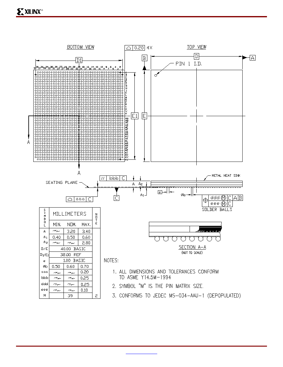
VirtexTM-II Platform FPGAs: Pinout Information
R
DS031-4 (v2.0) August 1, 2003
www.xilinx.com
Module 4 of 4
Product Specification
1-800-255-7778
197
FF1517 Flip-Chip Fine-Pitch BGA Package Specifications (1.00mm pitch)
Figure 9: FF1517 Flip-Chip Fine-Pitch BGA Package Specifications
VirtexTM-II Platform FPGAs: Pinout Information
R
DS031-4 (v2.0) August 1, 2003
www.xilinx.com
Module 4 of 4
Product Specification
1-800-255-7778
198
BF957 Flip-Chip BGA Package
As shown in
Table 14
, XC2V2000, XC2V3000, XC2V4000, and XC2V6000 Virtex-II devices are available in the BF957
package. Pins in each of these devices are the same, except for the pin differences in the XC2V2000 device shown in the
No Connect column. Following this table are the
BF957 Flip-Chip BGA Package Specifications (1.27mm pitch)
.
Table 14: BF957 -- XC2V2000, XC2V3000, XC2V4000, and XC2V6000
Bank
Pin Description
Pin Number
No Connect in XC2V2000
0
IO_L01N_0
H23
0
IO_L01P_0
H22
0
IO_L02N_0
G24
0
IO_L02P_0
E25
0
IO_L03N_0/VRP_0
B29
0
IO_L03P_0/VRN_0
C27
0
IO_L04N_0/VREF_0
F24
0
IO_L04P_0
F23
0
IO_L05N_0
D26
0
IO_L05P_0
D25
0
IO_L06N_0
A28
0
IO_L06P_0
A27
0
IO_L19N_0
J22
0
IO_L19P_0
J21
0
IO_L20N_0
G23
0
IO_L20P_0
G22
0
IO_L21N_0
B27
0
IO_L21P_0/VREF_0
B26
0
IO_L22N_0
K20
0
IO_L22P_0
K19
0
IO_L23N_0
C26
0
IO_L23P_0
C24
0
IO_L24N_0
D24
0
IO_L24P_0
D23
0
IO_L25N_0
E24
NC
0
IO_L25P_0
E23
NC
0
IO_L26N_0
G21
NC
0
IO_L26P_0
G20
NC
0
IO_L27N_0
A26
NC
0
IO_L27P_0/VREF_0
A25
NC
0
IO_L29N_0
H21
NC
0
IO_L29P_0
H20
NC
0
IO_L30N_0
B25
NC
0
IO_L30P_0
B23
NC

VirtexTM-II Platform FPGAs: Pinout Information
R
DS031-4 (v2.0) August 1, 2003
www.xilinx.com
Module 4 of 4
Product Specification
1-800-255-7778
199
0
IO_L49N_0
C23
0
IO_L49P_0
C22
0
IO_L50N_0
E22
0
IO_L50P_0
E21
0
IO_L51N_0
F21
0
IO_L51P_0/VREF_0
F20
0
IO_L52N_0
A24
0
IO_L52P_0
A23
0
IO_L53N_0
E20
0
IO_L53P_0
E19
0
IO_L54N_0
B22
0
IO_L54P_0
B21
0
IO_L67N_0
D21
0
IO_L67P_0
D20
0
IO_L68N_0
J20
0
IO_L68P_0
J19
0
IO_L69N_0
F19
0
IO_L69P_0/VREF_0
F18
0
IO_L70N_0
A22
0
IO_L70P_0
A21
0
IO_L71N_0
H19
0
IO_L71P_0
H17
0
IO_L72N_0
C21
0
IO_L72P_0
C20
0
IO_L73N_0
B20
0
IO_L73P_0
B19
0
IO_L74N_0
G18
0
IO_L74P_0
G17
0
IO_L75N_0
E18
0
IO_L75P_0/VREF_0
D17
0
IO_L76N_0
A20
0
IO_L76P_0
A19
0
IO_L77N_0
D19
0
IO_L77P_0
D18
0
IO_L78N_0
C19
0
IO_L78P_0
C17
0
IO_L91N_0/VREF_0
K18
0
IO_L91P_0
J18
Table 14: BF957 -- XC2V2000, XC2V3000, XC2V4000, and XC2V6000
Bank
Pin Description
Pin Number
No Connect in XC2V2000

VirtexTM-II Platform FPGAs: Pinout Information
R
DS031-4 (v2.0) August 1, 2003
www.xilinx.com
Module 4 of 4
Product Specification
1-800-255-7778
200
0
IO_L92N_0
F17
0
IO_L92P_0
F16
0
IO_L93N_0
B18
0
IO_L93P_0
B17
0
IO_L94N_0/VREF_0
J17
0
IO_L94P_0
J16
0
IO_L95N_0/GCLK7P
E17
0
IO_L95P_0/GCLK6S
E16
0
IO_L96N_0/GCLK5P
A18
0
IO_L96P_0/GCLK4S
A17
1
IO_L96N_1/GCLK3P
C16
1
IO_L96P_1/GCLK2S
C15
1
IO_L95N_1/GCLK1P
H16
1
IO_L95P_1/GCLK0S
H15
1
IO_L94N_1
A15
1
IO_L94P_1/VREF_1
A14
1
IO_L93N_1
F15
1
IO_L93P_1
F14
1
IO_L92N_1
G15
1
IO_L92P_1
G14
1
IO_L91N_1
B15
1
IO_L91P_1/VREF_1
B14
1
IO_L78N_1
D15
1
IO_L78P_1
E15
1
IO_L77N_1
J15
1
IO_L77P_1
K14
1
IO_L76N_1
D14
1
IO_L76P_1
D13
1
IO_L75N_1/VREF_1
E14
1
IO_L75P_1
E13
1
IO_L74N_1
A13
1
IO_L74P_1
A12
1
IO_L73N_1
F13
1
IO_L73P_1
F12
1
IO_L72N_1
J14
1
IO_L72P_1
J13
1
IO_L71N_1
B13
Table 14: BF957 -- XC2V2000, XC2V3000, XC2V4000, and XC2V6000
Bank
Pin Description
Pin Number
No Connect in XC2V2000

VirtexTM-II Platform FPGAs: Pinout Information
R
DS031-4 (v2.0) August 1, 2003
www.xilinx.com
Module 4 of 4
Product Specification
1-800-255-7778
201
1
IO_L71P_1
B12
1
IO_L70N_1
C13
1
IO_L70P_1
C12
1
IO_L69N_1/VREF_1
H13
1
IO_L69P_1
H12
1
IO_L68N_1
D12
1
IO_L68P_1
D11
1
IO_L67N_1
B11
1
IO_L67P_1
B10
1
IO_L54N_1
E12
1
IO_L54P_1
E11
1
IO_L53N_1
A11
1
IO_L53P_1
A10
1
IO_L52N_1
G12
1
IO_L52P_1
G11
1
IO_L51N_1/VREF_1
K13
1
IO_L51P_1
K12
1
IO_L50N_1
C11
1
IO_L50P_1
C10
1
IO_L49N_1
B9
1
IO_L49P_1
B7
1
IO_L30N_1
F11
NC
1
IO_L30P_1
F9
NC
1
IO_L29N_1
A9
NC
1
IO_L29P_1
A8
NC
1
IO_L27N_1/VREF_1
D9
NC
1
IO_L27P_1
D8
NC
1
IO_L26N_1
J12
NC
1
IO_L26P_1
J11
NC
1
IO_L25N_1
C9
NC
1
IO_L25P_1
C8
NC
1
IO_L24N_1
E10
1
IO_L24P_1
E9
1
IO_L23N_1
H11
1
IO_L23P_1
H10
1
IO_L22N_1
A7
1
IO_L22P_1
A6
1
IO_L21N_1/VREF_1
A5
Table 14: BF957 -- XC2V2000, XC2V3000, XC2V4000, and XC2V6000
Bank
Pin Description
Pin Number
No Connect in XC2V2000
VirtexTM-II Platform FPGAs: Pinout Information
R
DS031-4 (v2.0) August 1, 2003
www.xilinx.com
Module 4 of 4
Product Specification
1-800-255-7778
202
1
IO_L21P_1
A4
1
IO_L20N_1
G10
1
IO_L20P_1
G9
1
IO_L19N_1
B6
1
IO_L19P_1
C5
1
IO_L06N_1
C6
1
IO_L06P_1
D6
1
IO_L05N_1
H9
1
IO_L05P_1
G8
1
IO_L04N_1
D7
1
IO_L04P_1/VREF_1
E6
1
IO_L03N_1/VRP_1
E8
1
IO_L03P_1/VRN_1
E7
1
IO_L02N_1
F8
1
IO_L02P_1
F7
1
IO_L01N_1
B5
1
IO_L01P_1
B3
2
IO_L01N_2
F5
2
IO_L01P_2
G4
2
IO_L02N_2/VRP_2
G6
2
IO_L02P_2/VRN_2
H6
2
IO_L03N_2
D3
2
IO_L03P_2/VREF_2
E4
2
IO_L04N_2
K10
2
IO_L04P_2
K9
2
IO_L05N_2
D2
2
IO_L05P_2
E3
2
IO_L06N_2
F4
2
IO_L06P_2
F3
2
IO_L19N_2
L10
2
IO_L19P_2
M10
2
IO_L20N_2
H7
2
IO_L20P_2
J8
2
IO_L21N_2
D1
2
IO_L21P_2/VREF_2
E1
2
IO_L22N_2
G5
2
IO_L22P_2
H5
Table 14: BF957 -- XC2V2000, XC2V3000, XC2V4000, and XC2V6000
Bank
Pin Description
Pin Number
No Connect in XC2V2000

VirtexTM-II Platform FPGAs: Pinout Information
R
DS031-4 (v2.0) August 1, 2003
www.xilinx.com
Module 4 of 4
Product Specification
1-800-255-7778
203
2
IO_L23N_2
E2
2
IO_L23P_2
F2
2
IO_L24N_2
H4
2
IO_L24P_2
J4
2
IO_L25N_2
K8
NC
2
IO_L25P_2
L8
NC
2
IO_L27N_2
J7
NC
2
IO_L27P_2/VREF_2
K7
NC
2
IO_L43N_2
F1
2
IO_L43P_2
G1
2
IO_L44N_2
L9
2
IO_L44P_2
M9
2
IO_L45N_2
G2
2
IO_L45P_2/VREF_2
J2
2
IO_L46N_2
H3
2
IO_L46P_2
J3
2
IO_L47N_2
J6
2
IO_L47P_2
L6
2
IO_L48N_2
J5
2
IO_L48P_2
K5
2
IO_L49N_2
H1
2
IO_L49P_2
J1
2
IO_L50N_2
N10
2
IO_L50P_2
P10
2
IO_L51N_2
L7
2
IO_L51P_2/VREF_2
M7
2
IO_L52N_2
K3
2
IO_L52P_2
L3
2
IO_L53N_2
M8
2
IO_L53P_2
N8
2
IO_L54N_2
L5
2
IO_L54P_2
M5
2
IO_L67N_2
K2
2
IO_L67P_2
L2
2
IO_L68N_2
M6
2
IO_L68P_2
N6
2
IO_L69N_2
L4
2
IO_L69P_2/VREF_2
M4
Table 14: BF957 -- XC2V2000, XC2V3000, XC2V4000, and XC2V6000
Bank
Pin Description
Pin Number
No Connect in XC2V2000

VirtexTM-II Platform FPGAs: Pinout Information
R
DS031-4 (v2.0) August 1, 2003
www.xilinx.com
Module 4 of 4
Product Specification
1-800-255-7778
204
2
IO_L70N_2
K1
2
IO_L70P_2
L1
2
IO_L71N_2
N9
2
IO_L71P_2
P9
2
IO_L72N_2
N5
2
IO_L72P_2
P5
2
IO_L73N_2
M3
2
IO_L73P_2
N3
2
IO_L74N_2
R8
2
IO_L74P_2
R9
2
IO_L75N_2
M2
2
IO_L75P_2/VREF_2
N2
2
IO_L76N_2
M1
2
IO_L76P_2
N1
2
IO_L77N_2
P7
2
IO_L77P_2
R7
2
IO_L78N_2
N4
2
IO_L78P_2
P4
2
IO_L91N_2
T8
2
IO_L91P_2
T9
2
IO_L92N_2
P6
2
IO_L92P_2
R6
2
IO_L93N_2
P2
2
IO_L93P_2/VREF_2
R2
2
IO_L94N_2
R5
2
IO_L94P_2
T5
2
IO_L95N_2
P1
2
IO_L95P_2
R1
2
IO_L96N_2
R4
2
IO_L96P_2
R3
3
IO_L96N_3
T6
3
IO_L96P_3
U5
3
IO_L95N_3
U6
3
IO_L95P_3
V6
3
IO_L94N_3
T3
3
IO_L94P_3
U3
3
IO_L93N_3/VREF_3
U1
Table 14: BF957 -- XC2V2000, XC2V3000, XC2V4000, and XC2V6000
Bank
Pin Description
Pin Number
No Connect in XC2V2000

VirtexTM-II Platform FPGAs: Pinout Information
R
DS031-4 (v2.0) August 1, 2003
www.xilinx.com
Module 4 of 4
Product Specification
1-800-255-7778
205
3
IO_L93P_3
V1
3
IO_L92N_3
U8
3
IO_L92P_3
W8
3
IO_L91N_3
U2
3
IO_L91P_3
V2
3
IO_L78N_3
U7
3
IO_L78P_3
V7
3
IO_L77N_3
U4
3
IO_L77P_3
V4
3
IO_L76N_3
W1
3
IO_L76P_3
Y1
3
IO_L75N_3/VREF_3
V5
3
IO_L75P_3
W5
3
IO_L74N_3
W2
3
IO_L74P_3
Y2
3
IO_L73N_3
W6
3
IO_L73P_3
Y6
3
IO_L72N_3
Y5
3
IO_L72P_3
AA5
3
IO_L71N_3
W3
3
IO_L71P_3
Y3
3
IO_L70N_3
W4
3
IO_L70P_3
Y4
3
IO_L69N_3/VREF_3
U9
3
IO_L69P_3
V9
3
IO_L68N_3
AA1
3
IO_L68P_3
AB1
3
IO_L67N_3
Y7
3
IO_L67P_3
AA7
3
IO_L54N_3
AA6
3
IO_L54P_3
AC6
3
IO_L53N_3
AA2
3
IO_L53P_3
AB2
3
IO_L52N_3
AA4
3
IO_L52P_3
AC4
3
IO_L51N_3/VREF_3
V10
3
IO_L51P_3
W10
3
IO_L50N_3
AA3
Table 14: BF957 -- XC2V2000, XC2V3000, XC2V4000, and XC2V6000
Bank
Pin Description
Pin Number
No Connect in XC2V2000

VirtexTM-II Platform FPGAs: Pinout Information
R
DS031-4 (v2.0) August 1, 2003
www.xilinx.com
Module 4 of 4
Product Specification
1-800-255-7778
206
3
IO_L50P_3
AB3
3
IO_L49N_3
AB5
3
IO_L49P_3
AC5
3
IO_L48N_3
W9
3
IO_L48P_3
Y9
3
IO_L47N_3
AC1
3
IO_L47P_3
AD1
3
IO_L46N_3
AC3
3
IO_L46P_3
AD3
3
IO_L45N_3/VREF_3
Y8
3
IO_L45P_3
AA8
3
IO_L44N_3
AC2
3
IO_L44P_3
AE2
3
IO_L43N_3
AB7
3
IO_L43P_3
AC7
3
IO_L27N_3/VREF_3
Y10
NC
3
IO_L27P_3
AA10
NC
3
IO_L25N_3
AE1
NC
3
IO_L25P_3
AF1
NC
3
IO_L24N_3
AF2
3
IO_L24P_3
AG2
3
IO_L23N_3
AA9
3
IO_L23P_3
AB9
3
IO_L22N_3
AD4
3
IO_L22P_3
AE4
3
IO_L21N_3/VREF_3
AD5
3
IO_L21P_3
AE5
3
IO_L20N_3
AB8
3
IO_L20P_3
AC8
3
IO_L19N_3
AG1
3
IO_L19P_3
AH1
3
IO_L06N_3
AF4
3
IO_L06P_3
AG4
3
IO_L05N_3
AB10
3
IO_L05P_3
AB11
3
IO_L04N_3
AF3
3
IO_L04P_3
AG3
3
IO_L03N_3/VREF_3
AD6
Table 14: BF957 -- XC2V2000, XC2V3000, XC2V4000, and XC2V6000
Bank
Pin Description
Pin Number
No Connect in XC2V2000
VirtexTM-II Platform FPGAs: Pinout Information
R
DS031-4 (v2.0) August 1, 2003
www.xilinx.com
Module 4 of 4
Product Specification
1-800-255-7778
207
3
IO_L03P_3
AD7
3
IO_L02N_3/VRP_3
AE6
3
IO_L02P_3/VRN_3
AF5
3
IO_L01N_3
AH2
3
IO_L01P_3
AH3
4
IO_L01N_4/BUSY/DOUT
(1)
AD9
4
IO_L01P_4/INIT_B
AD10
4
IO_L02N_4/D0/DIN
(1)
AF7
4
IO_L02P_4/D1
AG7
4
IO_L03N_4/D2/ALT_VRP_4
AK3
4
IO_L03P_4/D3/ALT_VRN_4
AJ5
4
IO_L04N_4/VREF_4
AE8
4
IO_L04P_4
AF8
4
IO_L05N_4/VRP_4
AK4
4
IO_L05P_4/VRN_4
AK5
4
IO_L06N_4
AH6
4
IO_L06P_4
AH7
4
IO_L19N_4
AC10
4
IO_L19P_4
AC11
4
IO_L20N_4
AE9
4
IO_L20P_4
AE10
4
IO_L21N_4
AL4
4
IO_L21P_4/VREF_4
AL5
4
IO_L22N_4
AB12
4
IO_L22P_4
AB13
4
IO_L23N_4
AJ6
4
IO_L23P_4
AJ8
4
IO_L24N_4
AK6
4
IO_L24P_4
AK7
4
IO_L25N_4
AG8
NC
4
IO_L25P_4
AG9
NC
4
IO_L26N_4
AF9
NC
4
IO_L26P_4
AF11
NC
4
IO_L27N_4
AH8
NC
4
IO_L27P_4/VREF_4
AH9
NC
4
IO_L28N_4
AD11
NC
4
IO_L28P_4
AD12
NC
Table 14: BF957 -- XC2V2000, XC2V3000, XC2V4000, and XC2V6000
Bank
Pin Description
Pin Number
No Connect in XC2V2000

VirtexTM-II Platform FPGAs: Pinout Information
R
DS031-4 (v2.0) August 1, 2003
www.xilinx.com
Module 4 of 4
Product Specification
1-800-255-7778
208
4
IO_L29N_4
AL6
NC
4
IO_L29P_4
AL7
NC
4
IO_L30N_4
AJ9
NC
4
IO_L30P_4
AJ10
NC
4
IO_L49N_4
AE11
4
IO_L49P_4
AE12
4
IO_L50N_4
AG10
4
IO_L50P_4
AG11
4
IO_L51N_4
AL8
4
IO_L51P_4/VREF_4
AL9
4
IO_L52N_4
AF12
4
IO_L52P_4
AF13
4
IO_L53N_4
AK9
4
IO_L53P_4
AK10
4
IO_L54N_4
AH11
4
IO_L54P_4
AH12
4
IO_L67N_4
AC12
4
IO_L67P_4
AC13
4
IO_L68N_4
AG12
4
IO_L68P_4
AG13
4
IO_L69N_4
AL10
4
IO_L69P_4/VREF_4
AL11
4
IO_L70N_4
AD13
4
IO_L70P_4
AD15
4
IO_L71N_4
AJ11
4
IO_L71P_4
AJ12
4
IO_L72N_4
AK11
4
IO_L72P_4
AK12
4
IO_L73N_4
AE14
4
IO_L73P_4
AE15
4
IO_L74N_4
AF14
4
IO_L74P_4
AF15
4
IO_L75N_4
AL12
4
IO_L75P_4/VREF_4
AL13
4
IO_L76N_4
AB14
4
IO_L76P_4
AC14
4
IO_L77N_4
AH13
4
IO_L77P_4
AH14
Table 14: BF957 -- XC2V2000, XC2V3000, XC2V4000, and XC2V6000
Bank
Pin Description
Pin Number
No Connect in XC2V2000
VirtexTM-II Platform FPGAs: Pinout Information
R
DS031-4 (v2.0) August 1, 2003
www.xilinx.com
Module 4 of 4
Product Specification
1-800-255-7778
209
4
IO_L78N_4
AJ13
4
IO_L78P_4
AK13
4
IO_L91N_4/VREF_4
AC15
4
IO_L91P_4
AC16
4
IO_L92N_4
AG14
4
IO_L92P_4
AG15
4
IO_L93N_4
AK14
4
IO_L93P_4
AK15
4
IO_L94N_4/VREF_4
AF16
4
IO_L94P_4
AG16
4
IO_L95N_4/GCLK3S
AL14
4
IO_L95P_4/GCLK2P
AL15
4
IO_L96N_4/GCLK1S
AH15
4
IO_L96P_4/GCLK0P
AJ15
5
IO_L96N_5/GCLK7S
AJ16
5
IO_L96P_5/GCLK6P
AH17
5
IO_L95N_5/GCLK5S
AD16
5
IO_L95P_5/GCLK4P
AD17
5
IO_L94N_5
AL17
5
IO_L94P_5/VREF_5
AL18
5
IO_L93N_5
AG17
5
IO_L93P_5
AF17
5
IO_L92N_5
AE17
5
IO_L92P_5
AE18
5
IO_L91N_5
AK17
5
IO_L91P_5/VREF_5
AJ17
5
IO_L78N_5
AK18
5
IO_L78P_5
AK19
5
IO_L77N_5
AC17
5
IO_L77P_5
AB18
5
IO_L76N_5
AH18
5
IO_L76P_5
AH19
5
IO_L75N_5/VREF_5
AL19
5
IO_L75P_5
AL20
5
IO_L74N_5
AC18
5
IO_L74P_5
AC19
5
IO_L73N_5
AJ19
Table 14: BF957 -- XC2V2000, XC2V3000, XC2V4000, and XC2V6000
Bank
Pin Description
Pin Number
No Connect in XC2V2000

VirtexTM-II Platform FPGAs: Pinout Information
R
DS031-4 (v2.0) August 1, 2003
www.xilinx.com
Module 4 of 4
Product Specification
1-800-255-7778
210
5
IO_L73P_5
AJ20
5
IO_L72N_5
AG18
5
IO_L72P_5
AG19
5
IO_L71N_5
AF18
5
IO_L71P_5
AF19
5
IO_L70N_5
AK20
5
IO_L70P_5
AK21
5
IO_L69N_5/VREF_5
AH20
5
IO_L69P_5
AH21
5
IO_L68N_5
AD19
5
IO_L68P_5
AD20
5
IO_L67N_5
AL21
5
IO_L67P_5
AL22
5
IO_L54N_5
AG20
5
IO_L54P_5
AG21
5
IO_L53N_5
AB19
5
IO_L53P_5
AB20
5
IO_L52N_5
AJ21
5
IO_L52P_5
AJ22
5
IO_L51N_5/VREF_5
AF20
5
IO_L51P_5
AF21
5
IO_L50N_5
AE20
5
IO_L50P_5
AE21
5
IO_L49N_5
AK22
5
IO_L49P_5
AK23
5
IO_L30N_5
AJ23
NC
5
IO_L30P_5
AJ24
NC
5
IO_L29N_5
AC20
NC
5
IO_L29P_5
AC21
NC
5
IO_L28N_5
AL23
NC
5
IO_L28P_5
AL24
NC
5
IO_L27N_5/VREF_5
AL25
NC
5
IO_L27P_5
AL26
NC
5
IO_L26N_5
AD21
NC
5
IO_L26P_5
AD22
NC
5
IO_L25N_5
AH23
NC
5
IO_L25P_5
AH24
NC
5
IO_L24N_5
AG22
Table 14: BF957 -- XC2V2000, XC2V3000, XC2V4000, and XC2V6000
Bank
Pin Description
Pin Number
No Connect in XC2V2000
VirtexTM-II Platform FPGAs: Pinout Information
R
DS031-4 (v2.0) August 1, 2003
www.xilinx.com
Module 4 of 4
Product Specification
1-800-255-7778
211
5
IO_L24P_5
AG23
5
IO_L23N_5
AE22
5
IO_L23P_5
AE23
5
IO_L22N_5
AK25
5
IO_L22P_5
AK26
5
IO_L21N_5/VREF_5
AH25
5
IO_L21P_5
AG25
5
IO_L20N_5
AB21
5
IO_L20P_5
AC22
5
IO_L19N_5
AL27
5
IO_L19P_5
AL28
5
IO_L06N_5
AK27
5
IO_L06P_5
AJ27
5
IO_L05N_5/VRP_5
AD23
5
IO_L05P_5/VRN_5
AE24
5
IO_L04N_5
AJ26
5
IO_L04P_5/VREF_5
AH26
5
IO_L03N_5/D4/ALT_VRP_5
AF23
5
IO_L03P_5/D5/ALT_VRN_5
AF24
5
IO_L02N_5/D6
AG24
5
IO_L02P_5/D7
AF25
5
IO_L01N_5/RDWR_B
AK28
5
IO_L01P_5/CS_B
AK29
6
IO_L01P_6
AF27
6
IO_L01N_6
AF28
6
IO_L02P_6/VRN_6
AE26
6
IO_L02N_6/VRP_6
AE27
6
IO_L03P_6
AH29
6
IO_L03N_6/VREF_6
AH30
6
IO_L04P_6
AB22
6
IO_L04N_6
AB23
6
IO_L05P_6
AG28
6
IO_L05N_6
AG29
6
IO_L06P_6
AH31
6
IO_L06N_6
AG31
6
IO_L19P_6
AA22
6
IO_L19N_6
Y22
Table 14: BF957 -- XC2V2000, XC2V3000, XC2V4000, and XC2V6000
Bank
Pin Description
Pin Number
No Connect in XC2V2000
VirtexTM-II Platform FPGAs: Pinout Information
R
DS031-4 (v2.0) August 1, 2003
www.xilinx.com
Module 4 of 4
Product Specification
1-800-255-7778
212
6
IO_L20P_6
AD25
6
IO_L20N_6
AC24
6
IO_L21P_6
AG30
6
IO_L21N_6/VREF_6
AF30
6
IO_L22P_6
AD26
6
IO_L22N_6
AC26
6
IO_L23P_6
AF29
6
IO_L23N_6
AD29
6
IO_L24P_6
AE28
6
IO_L24N_6
AD28
6
IO_L25P_6
AB24
NC
6
IO_L25N_6
AA24
NC
6
IO_L27P_6
AC25
NC
6
IO_L27N_6/VREF_6
AB25
NC
6
IO_L43P_6
AF31
6
IO_L43N_6
AE31
6
IO_L44P_6
AA23
6
IO_L44N_6
Y23
6
IO_L45P_6
AE30
6
IO_L45N_6/VREF_6
AC30
6
IO_L46P_6
AC28
6
IO_L46N_6
AA28
6
IO_L47P_6
AD27
6
IO_L47N_6
AC27
6
IO_L48P_6
AA25
6
IO_L48N_6
Y25
6
IO_L49P_6
AC29
6
IO_L49N_6
AB29
6
IO_L50P_6
AB27
6
IO_L50N_6
AA27
6
IO_L51P_6
AA26
6
IO_L51N_6/VREF_6
Y26
6
IO_L52P_6
AD31
6
IO_L52N_6
AC31
6
IO_L53P_6
W22
6
IO_L53N_6
V22
6
IO_L54P_6
Y27
6
IO_L54N_6
W27
Table 14: BF957 -- XC2V2000, XC2V3000, XC2V4000, and XC2V6000
Bank
Pin Description
Pin Number
No Connect in XC2V2000

VirtexTM-II Platform FPGAs: Pinout Information
R
DS031-4 (v2.0) August 1, 2003
www.xilinx.com
Module 4 of 4
Product Specification
1-800-255-7778
213
6
IO_L67P_6
AB30
6
IO_L67N_6
AA30
6
IO_L68P_6
W26
6
IO_L68N_6
V26
6
IO_L69P_6
AB31
6
IO_L69N_6/VREF_6
AA31
6
IO_L70P_6
AA29
6
IO_L70N_6
Y29
6
IO_L71P_6
Y24
6
IO_L71N_6
W24
6
IO_L72P_6
V25
6
IO_L72N_6
U25
6
IO_L73P_6
Y28
6
IO_L73N_6
W28
6
IO_L74P_6
W23
6
IO_L74N_6
V23
6
IO_L75P_6
Y30
6
IO_L75N_6/VREF_6
W30
6
IO_L76P_6
Y31
6
IO_L76N_6
W31
6
IO_L77P_6
V27
6
IO_L77N_6
U27
6
IO_L78P_6
W29
6
IO_L78N_6
U29
6
IO_L91P_6
U23
6
IO_L91N_6
T23
6
IO_L92P_6
U26
6
IO_L92N_6
T26
6
IO_L93P_6
V28
6
IO_L93N_6/VREF_6
U28
6
IO_L94P_6
U24
6
IO_L94N_6
T24
6
IO_L95P_6
V30
6
IO_L95N_6
U30
6
IO_L96P_6
V31
6
IO_L96N_6
U31
7
IO_L96P_7
T27
Table 14: BF957 -- XC2V2000, XC2V3000, XC2V4000, and XC2V6000
Bank
Pin Description
Pin Number
No Connect in XC2V2000

VirtexTM-II Platform FPGAs: Pinout Information
R
DS031-4 (v2.0) August 1, 2003
www.xilinx.com
Module 4 of 4
Product Specification
1-800-255-7778
214
7
IO_L96N_7
R27
7
IO_L95P_7
R24
7
IO_L95N_7
N24
7
IO_L94P_7
T29
7
IO_L94N_7
R29
7
IO_L93P_7/VREF_7
R31
7
IO_L93N_7
P31
7
IO_L92P_7
R26
7
IO_L92N_7
P26
7
IO_L91P_7
R30
7
IO_L91N_7
P30
7
IO_L78P_7
R25
7
IO_L78N_7
P25
7
IO_L77P_7
R28
7
IO_L77N_7
P28
7
IO_L76P_7
N31
7
IO_L76N_7
M31
7
IO_L75P_7/VREF_7
R23
7
IO_L75N_7
P23
7
IO_L74P_7
N30
7
IO_L74N_7
M30
7
IO_L73P_7
P27
7
IO_L73N_7
N27
7
IO_L72P_7
P22
7
IO_L72N_7
N22
7
IO_L71P_7
N29
7
IO_L71N_7
M29
7
IO_L70P_7
N28
7
IO_L70N_7
M28
7
IO_L69P_7/VREF_7
N26
7
IO_L69N_7
M26
7
IO_L68P_7
L31
7
IO_L68N_7
K31
7
IO_L67P_7
M27
7
IO_L67N_7
L27
7
IO_L54P_7
N23
7
IO_L54N_7
M23
7
IO_L53P_7
L30
Table 14: BF957 -- XC2V2000, XC2V3000, XC2V4000, and XC2V6000
Bank
Pin Description
Pin Number
No Connect in XC2V2000

VirtexTM-II Platform FPGAs: Pinout Information
R
DS031-4 (v2.0) August 1, 2003
www.xilinx.com
Module 4 of 4
Product Specification
1-800-255-7778
215
7
IO_L53N_7
K30
7
IO_L52P_7
L28
7
IO_L52N_7
J28
7
IO_L51P_7/VREF_7
M24
7
IO_L51N_7
L24
7
IO_L50P_7
L29
7
IO_L50N_7
K29
7
IO_L49P_7
M25
7
IO_L49N_7
L25
7
IO_L48P_7
L26
7
IO_L48N_7
J26
7
IO_L47P_7
J31
7
IO_L47N_7
H31
7
IO_L46P_7
J29
7
IO_L46N_7
H29
7
IO_L45P_7/VREF_7
M22
7
IO_L45N_7
L22
7
IO_L44P_7
J30
7
IO_L44N_7
G30
7
IO_L43P_7
K27
7
IO_L43N_7
J27
7
IO_L27P_7/VREF_7
L23
NC
7
IO_L27N_7
K23
NC
7
IO_L25P_7
G31
NC
7
IO_L25N_7
F31
NC
7
IO_L24P_7
F30
7
IO_L24N_7
E30
7
IO_L23P_7
K25
7
IO_L23N_7
J25
7
IO_L22P_7
H28
7
IO_L22N_7
G28
7
IO_L21P_7/VREF_7
H27
7
IO_L21N_7
G27
7
IO_L20P_7
K24
7
IO_L20N_7
J24
7
IO_L19P_7
E31
7
IO_L19N_7
D31
7
IO_L06P_7
F28
Table 14: BF957 -- XC2V2000, XC2V3000, XC2V4000, and XC2V6000
Bank
Pin Description
Pin Number
No Connect in XC2V2000
VirtexTM-II Platform FPGAs: Pinout Information
R
DS031-4 (v2.0) August 1, 2003
www.xilinx.com
Module 4 of 4
Product Specification
1-800-255-7778
216
7
IO_L06N_7
E28
7
IO_L05P_7
K22
7
IO_L05N_7
K21
7
IO_L04P_7
F29
7
IO_L04N_7
E29
7
IO_L03P_7/VREF_7
H26
7
IO_L03N_7
H25
7
IO_L02P_7/VRN_7
G26
7
IO_L02N_7/VRP_7
F27
7
IO_L01P_7
D30
7
IO_L01N_7
D29
0
VCCO_0
C18
0
VCCO_0
C25
0
VCCO_0
F22
0
VCCO_0
H18
0
VCCO_0
L17
0
VCCO_0
L18
0
VCCO_0
L19
0
VCCO_0
L20
0
VCCO_0
M17
0
VCCO_0
M18
0
VCCO_0
M19
1
VCCO_1
C7
1
VCCO_1
C14
1
VCCO_1
F10
1
VCCO_1
H14
1
VCCO_1
L12
1
VCCO_1
L13
1
VCCO_1
L14
1
VCCO_1
L15
1
VCCO_1
M13
1
VCCO_1
M14
1
VCCO_1
M15
2
VCCO_2
G3
2
VCCO_2
K6
2
VCCO_2
M11
2
VCCO_2
N11
Table 14: BF957 -- XC2V2000, XC2V3000, XC2V4000, and XC2V6000
Bank
Pin Description
Pin Number
No Connect in XC2V2000

VirtexTM-II Platform FPGAs: Pinout Information
R
DS031-4 (v2.0) August 1, 2003
www.xilinx.com
Module 4 of 4
Product Specification
1-800-255-7778
217
2
VCCO_2
N12
2
VCCO_2
P3
2
VCCO_2
P8
2
VCCO_2
P11
2
VCCO_2
P12
2
VCCO_2
R11
2
VCCO_2
R12
3
VCCO_3
U11
3
VCCO_3
U12
3
VCCO_3
V3
3
VCCO_3
V8
3
VCCO_3
V11
3
VCCO_3
V12
3
VCCO_3
W11
3
VCCO_3
W12
3
VCCO_3
Y11
3
VCCO_3
AB6
3
VCCO_3
AE3
4
VCCO_4
Y13
4
VCCO_4
Y14
4
VCCO_4
Y15
4
VCCO_4
AA12
4
VCCO_4
AA13
4
VCCO_4
AA14
4
VCCO_4
AA15
4
VCCO_4
AD14
4
VCCO_4
AF10
4
VCCO_4
AJ7
4
VCCO_4
AJ14
5
VCCO_5
Y17
5
VCCO_5
Y18
5
VCCO_5
Y19
5
VCCO_5
AA17
5
VCCO_5
AA18
5
VCCO_5
AA19
5
VCCO_5
AA20
5
VCCO_5
AD18
5
VCCO_5
AF22
Table 14: BF957 -- XC2V2000, XC2V3000, XC2V4000, and XC2V6000
Bank
Pin Description
Pin Number
No Connect in XC2V2000
VirtexTM-II Platform FPGAs: Pinout Information
R
DS031-4 (v2.0) August 1, 2003
www.xilinx.com
Module 4 of 4
Product Specification
1-800-255-7778
218
5
VCCO_5
AJ18
5
VCCO_5
AJ25
6
VCCO_6
U20
6
VCCO_6
U21
6
VCCO_6
V20
6
VCCO_6
V21
6
VCCO_6
V24
6
VCCO_6
V29
6
VCCO_6
W20
6
VCCO_6
W21
6
VCCO_6
Y21
6
VCCO_6
AB26
6
VCCO_6
AE29
7
VCCO_7
G29
7
VCCO_7
K26
7
VCCO_7
M21
7
VCCO_7
N20
7
VCCO_7
N21
7
VCCO_7
P20
7
VCCO_7
P21
7
VCCO_7
P24
7
VCCO_7
P29
7
VCCO_7
R20
7
VCCO_7
R21
NA
CCLK
AJ4
NA
PROG_B
D27
NA
DONE
AG6
NA
M0
AH27
NA
M1
AJ28
NA
M2
AG26
NA
HSWAP_EN
E26
NA
TCK
K11
NA
TDI
C28
NA
TDO
C4
NA
TMS
J10
NA
PWRDWN_B
AH5
NA
DXN
F25
Table 14: BF957 -- XC2V2000, XC2V3000, XC2V4000, and XC2V6000
Bank
Pin Description
Pin Number
No Connect in XC2V2000
VirtexTM-II Platform FPGAs: Pinout Information
R
DS031-4 (v2.0) August 1, 2003
www.xilinx.com
Module 4 of 4
Product Specification
1-800-255-7778
219
NA
DXP
B28
NA
VBATT
D5
NA
RSVD
B4
NA
VCCAUX
B16
NA
VCCAUX
C2
NA
VCCAUX
C30
NA
VCCAUX
T2
NA
VCCAUX
T30
NA
VCCAUX
AJ2
NA
VCCAUX
AJ30
NA
VCCAUX
AK16
NA
VCCINT
K15
NA
VCCINT
K17
NA
VCCINT
L11
NA
VCCINT
L16
NA
VCCINT
L21
NA
VCCINT
M12
NA
VCCINT
M16
NA
VCCINT
M20
NA
VCCINT
N13
NA
VCCINT
N14
NA
VCCINT
N15
NA
VCCINT
N16
NA
VCCINT
N17
NA
VCCINT
N18
NA
VCCINT
N19
NA
VCCINT
P13
NA
VCCINT
P19
NA
VCCINT
R10
NA
VCCINT
R13
NA
VCCINT
R19
NA
VCCINT
R22
NA
VCCINT
T11
NA
VCCINT
T12
NA
VCCINT
T13
NA
VCCINT
T19
NA
VCCINT
T20
Table 14: BF957 -- XC2V2000, XC2V3000, XC2V4000, and XC2V6000
Bank
Pin Description
Pin Number
No Connect in XC2V2000

VirtexTM-II Platform FPGAs: Pinout Information
R
DS031-4 (v2.0) August 1, 2003
www.xilinx.com
Module 4 of 4
Product Specification
1-800-255-7778
220
NA
VCCINT
T21
NA
VCCINT
U10
NA
VCCINT
U13
NA
VCCINT
U19
NA
VCCINT
U22
NA
VCCINT
V13
NA
VCCINT
V19
NA
VCCINT
W13
NA
VCCINT
W14
NA
VCCINT
W15
NA
VCCINT
W16
NA
VCCINT
W17
NA
VCCINT
W18
NA
VCCINT
W19
NA
VCCINT
Y12
NA
VCCINT
Y16
NA
VCCINT
Y20
NA
VCCINT
AA11
NA
VCCINT
AA16
NA
VCCINT
AA21
NA
VCCINT
AB15
NA
VCCINT
AB17
NA
GND
A2
NA
GND
A3
NA
GND
A16
NA
GND
A29
NA
GND
A30
NA
GND
B1
NA
GND
B2
NA
GND
B8
NA
GND
B24
NA
GND
B30
NA
GND
B31
NA
GND
C1
NA
GND
C3
NA
GND
C29
NA
GND
C31
NA
GND
D4
Table 14: BF957 -- XC2V2000, XC2V3000, XC2V4000, and XC2V6000
Bank
Pin Description
Pin Number
No Connect in XC2V2000

VirtexTM-II Platform FPGAs: Pinout Information
R
DS031-4 (v2.0) August 1, 2003
www.xilinx.com
Module 4 of 4
Product Specification
1-800-255-7778
221
NA
GND
D10
NA
GND
D16
NA
GND
D22
NA
GND
D28
NA
GND
E5
NA
GND
E27
NA
GND
F6
NA
GND
F26
NA
GND
G7
NA
GND
G13
NA
GND
G16
NA
GND
G19
NA
GND
G25
NA
GND
H2
NA
GND
H8
NA
GND
H24
NA
GND
H30
NA
GND
J9
NA
GND
J23
NA
GND
K4
NA
GND
K16
NA
GND
K28
NA
GND
N7
NA
GND
N25
NA
GND
P14
NA
GND
P15
NA
GND
P16
NA
GND
P17
NA
GND
P18
NA
GND
R14
NA
GND
R15
NA
GND
R16
NA
GND
R17
NA
GND
R18
NA
GND
T1
NA
GND
T4
NA
GND
T7
NA
GND
T10
Table 14: BF957 -- XC2V2000, XC2V3000, XC2V4000, and XC2V6000
Bank
Pin Description
Pin Number
No Connect in XC2V2000

VirtexTM-II Platform FPGAs: Pinout Information
R
DS031-4 (v2.0) August 1, 2003
www.xilinx.com
Module 4 of 4
Product Specification
1-800-255-7778
222
NA
GND
T14
NA
GND
T15
NA
GND
T16
NA
GND
T17
NA
GND
T18
NA
GND
T22
NA
GND
T25
NA
GND
T28
NA
GND
T31
NA
GND
U14
NA
GND
U15
NA
GND
U16
NA
GND
U17
NA
GND
U18
NA
GND
V14
NA
GND
V15
NA
GND
V16
NA
GND
V17
NA
GND
V18
NA
GND
W7
NA
GND
W25
NA
GND
AB4
NA
GND
AB16
NA
GND
AB28
NA
GND
AC9
NA
GND
AC23
NA
GND
AD2
NA
GND
AD8
NA
GND
AD24
NA
GND
AD30
NA
GND
AE7
NA
GND
AE13
NA
GND
AE16
NA
GND
AE19
NA
GND
AE25
NA
GND
AF6
NA
GND
AF26
NA
GND
AG5
Table 14: BF957 -- XC2V2000, XC2V3000, XC2V4000, and XC2V6000
Bank
Pin Description
Pin Number
No Connect in XC2V2000

VirtexTM-II Platform FPGAs: Pinout Information
R
DS031-4 (v2.0) August 1, 2003
www.xilinx.com
Module 4 of 4
Product Specification
1-800-255-7778
223
NA
GND
AG27
NA
GND
AH4
NA
GND
AH10
NA
GND
AH16
NA
GND
AH22
NA
GND
AH28
NA
GND
AJ1
NA
GND
AJ3
NA
GND
AJ29
NA
GND
AJ31
NA
GND
AK1
NA
GND
AK2
NA
GND
AK8
NA
GND
AK24
NA
GND
AK30
NA
GND
AK31
NA
GND
AL2
NA
GND
AL3
NA
GND
AL16
NA
GND
AL29
NA
GND
AL30
Notes:
1.
See
Table 4
for an explanation of the signals available on this pin.
Table 14: BF957 -- XC2V2000, XC2V3000, XC2V4000, and XC2V6000
Bank
Pin Description
Pin Number
No Connect in XC2V2000
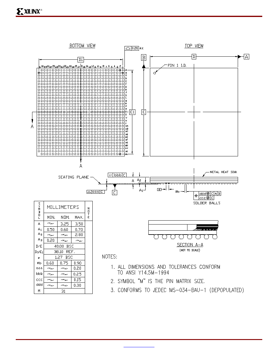
VirtexTM-II Platform FPGAs: Pinout Information
R
DS031-4 (v2.0) August 1, 2003
www.xilinx.com
Module 4 of 4
Product Specification
1-800-255-7778
224
BF957 Flip-Chip BGA Package Specifications (1.27mm pitch)
Figure 10: BF957 Flip-Chip BGA Package Specifications

VirtexTM-II Platform FPGAs: Pinout Information
R
DS031-4 (v2.0) August 1, 2003
www.xilinx.com
Module 4 of 4
Product Specification
1-800-255-7778
225
Revision History
This section records the change history for this module of the data sheet.
Virtex-II Data Sheet
The Virtex-II Data Sheet contains the following modules:
∑
VirtexTM-II Platform FPGAs: Introduction and Overview
(Module 1)
∑
VirtexTM-II Platform FPGAs: Detailed Description
(Module 2)
∑
VirtexTM-II Platform FPGAs: DC and Switching
Characteristics (Module 3)
∑
VirtexTM-II Platform FPGAs: Pinout Information
(Module 4)
Date
Version
Revision
11/07/00
1.0
Early access draft.
11/22/00
1.1
Initial Xilinx release. Made the following corrections:
CS144 package -
Table 5, page 5
:
∑
Added missing pin D10 in Bank 1.
∑
Changed dedicated pins A2 and B2 to RSVD (from DXN and DXP).
FG256 package -
Table 6, page 10
:
∑
Changed dedicated pins A3 and A4 to RSVD (from DXN and DXP).
FG896 package -
Table 11, page 94
:
∑
Corrected pin AG1 in Bank 4 to be AG12.
FF1152 package -
Table 12, page 120
:
∑
Corrected pin Y3 in Bank 6 to be Y32.
12/19/00
1.2
Reverse designations were fixed for pins in every package.
01/25/01
1.3
The data sheet was divided into four modules (per the current style standard). DXN and
DXP pin information was added for the CS144 package (
Table 5
) and the FG256 package
(
Table 6
).
02/07/01
1.4
DXN and DXP pin information was changed back to RSVD for the CS144 package (
Table 5
)
and the FG256 package (
Table 6
).
04/02/01
1.5
∑
ALT_VRN and ALT_VRP pin information was added for each package.
∑
Table 8, page 34
≠ added No Connect designations for the XC2V1500 device in the
FG676 package.
∑
Reverted to traditional double-column format.
11/07/01
1.6
∑
Updated list of devices supported in the FF1152, FF1517, and BF957 packages.
09/26/02
1.7
∑
Updated
Table 3
to reflect devices supported in the BG728 and BF957 packages.
∑
Added mention of LVPECL to pin definition in
Table 4
.
10/07/02
1.8
∑
Corrected
Table 10
heading to reflect supported devices in the BG728 package.
12/06/02
1.8.1
∑
Enhanced the description of the PWRDWN_B pin in
Table 4
.
05/07/03
1.8.2
∑
Added clarification to
Table 4
and all device pinout tables regarding the dual-use
nature of pins D0/DIN and BUSY/DOUT during configuration.
06/19/03
1.8.3
∑
The final GND pin in each of five pinout tables was inadvertently deleted in v1.8.2. This
revision restores the deleted GND pins as follows:
-
Pin C5,
Table 5, page 5
(CS144)
-
Pin A1,
Table 6, page 10
(FG256)
-
Pin A2,
Table 10, page 72
(BG728)
-
Pin A2,
Table 12, page 120
(FF1152)
-
Pin AL30,
Table 14, page 198
(BF957)
08/01/03
2.0
All Virtex-II devices and speed grades now Production. See Table 13, Module 3.